Note: Descriptions are shown in the official language in which they were submitted.
~ '3
R~_A~L~ LL~L~ b
Puls~ Width Modulato~
Technical Field
The presen~ invention relates generally to
~ RF-AM transmitters includiny pulse width modulators
driving an RF amplifier by way of a DC circuit
including a low pass filter and a power amplifier
driven by a pulse width modulated information
; indicating signal. In one particular aspect of the
invention, a tendency for stray capacity of an
` amplifier system including the power amplirier and the
``~ lS RF amplifier to lengthen the duration of short duration
~' pulse width modulated pulses is overcome by reducing
:~ the amplitude of only short duration pulses applied to
the power amplifier. In accordance with a further
aspect of the invention, a tendency of the RF amplifier
~0 to load the power amplifier out of saturation during
portions of pulses wider than the narrow pulses is
overcome by coupling the pulse width mod~lated signal
to the power amplifier grid by connecting a resistor
shunted by an inductor between the output of the pulse
- 25 width modulator and the power amplifier.
.,
. Baçkground ~rt
. ,s
:;
Swanson, U.S. Patents 3,506,920 and 3,S88,744
discloses a radio frequency tRF), amplitude modulated
~ (AM) transmitter wherein a D~ path is provided between
an anode-cathode circuit of an RF amplifier responsive
to an RF carrier and the anode-cathode path of a power
'~','.1
iJ~
amplifler responsive to a pulse width modulated
information representing signal. A low pass filter is
connected between the power amplifier and the RF
amplifier to smooth the pulse width modulated wave
driving the power amplifier into a variable amplitude
- signal that controls the power supply voltage for the
RF amplifier anode-cathode circuit.
The amplifying system including the power
amplifier and the RF amplifier of the Swanson patent
10 has stray capacity, including the shunt (anode-cathode)
- capacitance of the power amplifier tube. The stray
- capacity causes narrow pulses driving the power
: amplifier grid to be increased in length, whereby the
amplitude of an RF output of the RF amplifier has a
15 tendency to be greater than it should be in response to
-` these narrow width pulses. The power amplifier, being
- alternately driven into cutoff and saturation by the
- pulse width modulated signal applied to the grid
thereof, causes an excessively high amplitude power
supply voltage to be supplied to the RF amplifier
anode-cathode path by the low pass filter in response
- to the lengthened short duration pulses.
~; While the stray capacity lengthens and therefore
distorts all transitions and pulses of the pulse width
~ .
modulated signal applied to the power amplifier grid,
the amount of lengthening is insignificant for
relatively wide pulses compared with the total area of
such wide pulses. However, for shorter width pulses,
`~ which represent the information signal during high
level modulation in each negative half-cycle, the
;:~ distortion is usually appreciable.
~- In the Swanson patents, the distortion is, to
a certain extent, compensated by including a low pass
filter circuit in an amplifier driving the power
,, .
~, .
;~ `"
~i
~ ~if~
amplifier. The low pass filter circuit includes a
' capacitor shunting the anode-cathode path vf a pentode
amplifier and a resistor shunted by an inductor in
series between the plate of the pentode and a DC power
supply circuit for the pentode. The low pass filter
circuit reduces the amplitude of many of the pulses
supplied to the power amplifier during each cycle of an
information signal. In fact, the amplitude of only the
very longest pulses remains constant in the prior art
` 10 system disclosed in the Swanson patents.
Because the amplitude of many of the pulses
supplied to the power amplifier tube grid of Swanson
.: are reduced in amplitude, the efficiency of the
; transmiter is substantially reduced. This is because
-` 15 the amplifying system including the power amplifier and
; RF amplifier are operated most efficiently when the
; power amplifier is driven fully between cutoff and deep
- saturation.
~ It is, therefore, an object of the present
-1 20 invention to provide an R~, AM transmitter responsive
- to a pulse width modulated information representing
signal, with a new and improved circuit for
-~ compensating for stray capacity efEects of an
ampliEying system including a power amplifier and an RF
1 25 amplifier.
:'!' . Another object of the invention is to provide
an RF, AM transmitter responsive to a pulse width
' modulated information representing signal for
selectively reducing the magnitude of short duration
pulses to compensate for stray capacity effects of an
amplifying system, without changing the magnitude of
longer pulses to enable the amplifying system to
operate with greater efficiency since the power
`
.
.:~
, f ;~ Y~
.; amplifier is more consistently driven between deep
- sat~ration and cutoff.
An additional object of the present invention is
to provide an RF, AM transmitter responsive to a pulse
width mod~lated information representing signal source
wherein amplitude control of pulses applied to an
amplifying system of the transmitter is restricted to
short duration pulses in such a manner that the effect
of stray capacity of the amplifying system to lengthen
only the short duratlon pulses is obviated.
;................. A further object o~ the invention is to
~: provide an RF, AM transmitter including a power
.~ ampli~ier driving an anode-cathode circuit of an RF
; trans~itting tube by way of a DC circuit including a
low pass filter that converts a pulse width modulated
information signal applied to a grid of the power
:;, amplifier into a variable amplitude modulating signal
.. for the RF amplifier, wherein stray capacity of the
~; amplifying system that has a tendency to distort the RF
amplifier for low amplitude levels of the information
~ signal is obviated by modifying the amplitude of only
-; the short duration pulses.
. ~5 Disclosu~e of.InyQniinn
In accordance with one aspect of the present
., invention, a radio transmitter for transmitting an RF
i carrier amplitude modulated by an information signal
; 30 comprises a pulse width modulator responsive to the
. information signal for deriving a pulse width modulated
;- signal having pulses with widths representing the
amplitude of the information signal, wherein only
pulses having widths less than a predetermined short
, ,
~..
duration are reduced in amplitude. An amplifying
system includes a power amplifier responsive to the
~; pulse width modulated signal and a variable impedance
~ DC path forming part oE a power supply circuit of an RF
amplifier responsive to the carrier. The amplifying
system includes a low pass filter for converting pulses
derived by the power amplifier into a variable
amplitude signal DC coupled to the RF amplifierO
Preferably the power and RF amplifiers
- 10 respectively include first and second vacuum tubes so
` that an anode-cathode path of the first tube is
connected in a B+ supply circuit for anode-cathode path
of the second tube. The first tube is biased so it is
driven between saturation and cutoff in response to the
pùlses being and not being derived by the pulse width
~ modulator. The amplifier system has stray capacitance
y including shunt capacity of the first tube. The stray
capacity causes transitions o~ the pulses coupled to
the control grid of the first tube to be changed in
.
shape so that narrow ones of said pulses have a
tendency to be excessively long and have excessive
- energy to cause the carrier to have excessively high
instantaneous amplitude. In accordance with the
invention the amplitude of the narrow pulses ls reduced
so that the tendency thereof to have excessive energy
' is substantially obviated.
~; The amplitude of only the short duration
pulses is reduced by shuntin~ a grid of the first tube
with a resistor-capacitor charging circuit. A switch
responds to current flowing through the resistor-
capacitor circuit to provide (a) a low impedance path
from the grid to a reference potential terminal when
~ current initially flows in the resistor-capacitor
- circuit during a transition in each of the pulses and
--- 6
,, .
throughout the length of each of the short duration
pulses so that the power amplifier tube is forward
biased but not driven into saturation during the short
duration pulses, and ~b) a higher impedance path from
the grid to the reference potential after the
i transition and the time required for the short duration
pulses so that the first tube is driven into saturation
after the time required for the short duration pulses.
Because the first tube is driven into saturation during
all pulses longer than the short duration pulses,
rather than only during the longest pulses, greater
efficiency is provided by the present invention than is
~ attained with Swanson.
~~ The second tube, i.e., the tube included in
~,
t 15 the RF power amplifer, has a tendency to load the first
;~ tube out of saturation during latter portions of pulses
. . .
` considerably wider than the narrow pulses. This occurs
`.- when the second tube is driven to the maximum extent
- during the peak value of the low pass filter output
amplitude modulating it, as occurs when the information
', signal has a maximum positive instantaneous amplitude.
- Because of the loading effect, there is a tendency for
:- the first tube to be driven out of saturation when the
information signal has the greatest instantaneous
positive amplitude which causes the pulses applied to
~- the first tube to have the greatest length. Hence, the
carrier output of the RF amplifier has a tendency to
;~ have a lower amplitude than it should have at the time
of the greatest power demand by the RP amplifier.
: 30 The present invention provides a means
-`~ coupled to the amplifying system for maintaining the
amplitude of the wider pulses substantially constant
: throughout the duration thereof so that the tendency of
- the wide pulses to not drive the power amplifier into
:
.
saturatlon is substantially overcome. The circuitry
for maintaining the amplitude of the wider pulses
substantially constant throughout the duration thereof
includes a resistor shunted by an ind~ctor connected
- 5 between the pulse width modulator output and the grid
of the first tube. At the beginning of each pulse, the
inductor has a relatively high impedance to the high
frequency components in the transition and has no
ef~ect on the current flowing from the pulse width
modulator to the grid of the first tube. After the
. length of time associated with a short duration pulse
has elapsed, the impedance of the inductor decreases
substantially and effectively short circuits the
resistor, to supply a constant high level voltage and
:` 15 current to the grid of the first tube, to maintain the
; first tube in saturation.
:: The above and still further objects, features
.~i;
; and advantages of the present invention will become
~ apparent upon consideration of the following detailed
`l 20 description of one specific embodiment thereof,
~` especially when taken in conjunction with the
accompanyiny drawings.
,. .
. .
~i~f DescLip~on of th~D~wings
,~ .
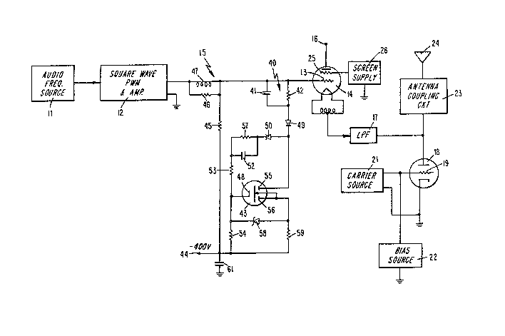
Fig. 1 is a partial circuit and partial block
~; diagram of a preferred embodiment of the present
~ invention; and
- 30 Figs. 2, 3, 4 and 5 are waveforms helpful in
~ ~ describing the operation of the circuit of Fig. 1.
'
"
, .
~ .
,~
::,..
?~
~dg_fQJ Carryil~ Q~t the InventiQn
Reference is now made to Fig. 1 of the
drawing wherein the preferred embodiment of the radio
frequency, amplitude modulated transmitter of the
- invention is illustrated as including an audio
frequency signal source 11 which drives square wave
pulse width modulator and amplifier 12, having a high
output impedance. Amplifier 12 drives grid 13 of power
pulse amplifier tube 14 by way of pulse shaping network
~ 15. Tube 14 has an anode-cathode path connected to B+
terminal 16 that is DC coupled by way of low pass
filter 17 to the anode-cathode circuit of radio
- frequency power amplifier tube 18 having grid 19
connected to radio frequency carrier source 21 and to
DC bias source 22. The anode-cathode circuit of tube
~: 18 includes antenna coupling circuit 23 which is
connected to antenna 24. Each of the elements
.~.
:~ illustrated in Fig. 1, except shaping circuit 15, is
- 20 old in the art, as disclosed, for example, in the
-- aforementioned Swanson patents.
Details of the operation of Fig. 1 are now
described, assuming that pulse shaping circuit 15 is
not provided.
; 25 Audio frequency source 11 can be any suitable
- source, such as speech, music, sinusoidal tones, square
waves, triangular waves, or variations thereof.
Several times during each cycle of source 11, square
~` wave pulse width modulator and ampliier 12 derives a
; 3o pulse having a duration that is a function of the
- instantaneous amplitude of source 11. The output of
square wave pulse width modulator and amplifier 12 is a
bilevel signal, having a constant positive voltage,
alternating with zero voltage levels. Relatively long
. .
..,
~,
.~
- positive and zero voltage levels are derived at the
` output of square wave pulse width modulator and
amplifier 12 in response to the instantaneous output of
source 11 being high and low, respectively.
; 5 The bias voltage applied to grid 13 of power
pulse amplifier tube 14 and the amplitude of the pulse
output of square wave pulse width modulator and
amplifier 12 are such that the anode-cathode path of
tube 14 is alternately driven between hard saturation
: 10 and cutoff. Thereby, a constant, relatively high
current level flows from B+ terminal 16 through the
anode~cathode path of tube 14 to low pass filter 17 and
the anode-cathode path of tube 18 while a positive
pulse amplitude is derived by square wave pulse width
~, 15 modulator and amplifier 12. In contrast, no current
~- flows from B+ terminal 16 to low pass filter 17 while
tube 14 is backbiased, i.e., cutoff, by the bias
voltage applied to grid 13 at the time a zero voltage
. level is derived from square wave pulse width modulator
;~ 20 and amplifier 12.
Low pass filter 17 responds to the variable
duration relatively high current pulses supplied to it
by way of the anode-cathode path of tube 13, to convert
; these current pulses into a relatively high current
level that is supposed to be a replica of the current
waveform of audio frequency source 11. The output of
low pass filter 17 which is supposed to be replica of
. the waveform of audio frequency source 11 controls the
impedance of the anode-cathode circuit of tube 18 and
- 30 loading of antenna coupling circuit 23.
Preferably, the amplitudes of carrier source
21 and bias source 22 are such that tube 18 operates in
Class C to provide maximum operating efficiency. It is
- to be understood~ however, that carrier source 21 and
,
.~..
/
bias source 22 can be connected to grid 19 in such a
manner as to cause tube 18 to operate in Class AB or
Class B operation.
-; Preferably, pulse power amplifier tube 14 is
a tetrode, having a screen ~rid 25 appropriately
energized by DC bias circuit 26. Despite the fact that
- power pulse amplifier tube 14 is a tetrode, it has
appreciable shunt capacitance between the anode and
cathode thereof. In addition, there is additional
stray capacitance in the amplifier system including
t~bes 14 and 18 and the circuitry associated therewith.
~.
This stray capacity associated with the amplifying
system is coupled back to the output terminals of
-` square wave pulse width modulator and amplifier 12. As
~ 15 a result of the stray capacity at the output terminals
- of square wave pulse width modulator and amplifier 12,
;~ transitions in the output pulse waveform of square wave
pulse width modulator amplifier 12 do not have the
~l idealized vertical wave shape. The shortest duration
pulses which are derived by circuit 12 during the
maximum negative peak portions of the highest amplitude
cycles of audio frequency source 11 have a tendency to
be lengthen~d to such an extent that when they are
smoothed or integrated by low pass filter 17 an
i~accurate replica of the wave shape of audio frequency
source 11 is applied as a modulating voltage for the
anode-cathode path of tuhe 18.
- An example of the effect of the short
duration pulses is illustrated in the waveforms of
Figs. 2-4, based upon the assumption that audio
~ -frequency source 11 is deriving a sinusoidal wave
-- shape, one cycle of which is illustrated as waveform
~` 31, Fig. 2. Square wave pulse width modulator and
.: .
~''' ` ' .
~..,,~.
amplifier li responds to waveform 31 to derive A pulse
width modulated wave shape.
An idealized output waveform of circuit 12 in
response to waveform 31 is illustrated in Fig. 3 as
square wave 32. Square wave 32 has a zero base and
vertical leading and trailing transitional edges and a
constant amplitude high voltage level. In response to
the positive half-cycle of sinusoidal waveform 31,
square wave 32 has relatively long duration positive,
constant amplitude levels, interspersed with short
duration zero amplitude levels. As the amplitude of
waveform 31 decreases, the durations of the positive
and zero levels of square wave 32 respectively decrease
and increase. When waveform 31 has a peak negative
voltage, the durations of the positive portions of
square wave 32 are much less than the durations of the
zero amplitude levels of the square wave~
If it is assumed that shaping circuit 15 is
not provided, the stray capacity of the amplifying
system, as reflected to the output terminals of sguare
wave pulse width modulator and amplifier 12, causes the
output of the modulator and amplifier 12 to be
distorted, as illustrated in Fig. 4 by waveform 34.
From Fig. 4 it is noted that the vertical transitions
of the leading and trailing edges of square wave 32 are
converted into waveforms having appreciable slope. The
slopes in the transitions of waveform 34 occur because
the stray shunt capacity across the output terminals of
modulator and amplifier 12 cannot respond instantly to
the transitions of square wave 32. The sloping
transitions of waveform 34 increase the area under each
pulse, i.e., the area between the positive value of the
pulse and the zero base line thereof.
~.
.s
~' .
.-.,~
1 - 12 -
3~ iJf~6'3
Because the area under each of the p~lses of
waveform 34 is increased, the amplitude of the output
of low pass filter 17 is not as accurate a replica of
audio frequency source 11 as is desired. The amplitude
. 5 modulated wave coupled to antenna 24 is thereby
distorted, such that there is a greater amount of
energy transmitted by the antenna to represent the
instantaneous audio frequency source variations. The
distortion is not particularly noticeable when
~-; 10 information signal 3i has a high amplitude and the
pulses derived by modulator and amplifier 12 are
relatively long. This is because the percentage of the
area added to these pulses due to the sloping
transitions is not appreciable. However, for short
duration pulses, i.e.l pulses having a duration less
than a predetermined interval, e.g. 10 microseconds,
the percent distortion is enough to appreciably
adversely affect the nature of the transmitted signal.
` In particular, pulse 33 in idealized square wave 32, as
occurs in proximity to the minimum value of waveform
31, is distorted signiicantly, as indicated by
distorted pulse 35. The area under the curve of pulse
35 is an appreciable percentage, such as 33%, greater
-~ than the area under idealized pulse 33.
-; 25 In accordance with the present invention,
; shaping network 15 responds to the output of modulator
and amplifier 12, as represented by waveform 34~ to
decrease the amplitude of only those short duration
pulses having an area increase sufficiently great to
cause significan~ distortion in the output of the AM
wave transmitted from antenna 24. The amplitude
- decrease caused by circuit 15 i5 sufficient to cause
power pulse amplifier tube 14 to be driven out of
saturation, but not into cutoff, in response to the
., ~
.
'~
! - 13 -
short duration pulses. Thereby, the current coupled by
amplifier 14 to low pass filter 17 in response to each
short duratîon output pulse of modulator and amplifier
- 12, when smoothed or integrated by filter 17, causes an
accurate replica of source 11 to be coupled to the DC
power supply for the anode-cathode circuit of tube 18
and antenna coupling circuit 23. Because power pulse
amplifier tube 14 is driven to saturation by all output
~ pulses of modulator and amplifier 12 other than those
; 10 few pulses which have a short enough duration to cause
-~ appreciable distortion in the output of low pass filter
~ 17, tube 14 is operated with optimum efficiency.
-: - Circuit 15 thus responds to waveform 34 to
derive waveform 36 (Fig 5) which is coupled to grid 13
- 15 of power pulse amplifier tube 14. From waveform 36, it
is noted that the amplitude of each pulse of waveorm
34, except pulse 35, is preserved. The amplitude of
pulse 35 is reduced, as indicated by pulse 37.
Circuit 15 basically includes a charging
circuit 40 comprising the parallel combination of
~ capacitor 41 and resistor 42 in shunt with the output
-~ of modulator and amplifier 12 and grid 13 of power
pulse amplifier tube 14. Circuit 40 is connected to a
`^ switch in the form of the source drain path of field
effect transistor 43. During each transition in the
-~ output of modulator and amplifier 12 and during each of
the short duration pulses, such as pulse 35, switch 43
`i is closed to provide a low impedance path for the
~ output of the modulator and amplifier, so that tube 14
--I 30 is not driven into saturation. At the time associated
- with the short duration pulses terminating~ switch 43
is open and the full output voltage of modulator and
amplifier 12 is applied to grid 13~
.
'~,
In the preferred embodiment, the output vf
modulator and amplifier 12 varies between zero and +659
- volts, and a negative 400 volt DC level at terminal 44
is connected via a variable impedance DC path to yrid
~:: 5 13 of tube 14. The bias voltage at terminal 44 is DC
coupled to grid 13 by way of bias resistor 45.
Thereby, the anode-cathode path of amplifier tube 14 is
maintained at cutoff while a zero level is derived from
modulator and amplifier 12, hut is driven into hard
saturation because of the 250 volt positive bias
~ applied across resistor 45 when the modulator and
`~ amplifier derives a high, 650 volt output level.
` The voltage variations at the output of
modulator and amplifier 12 are coupled to grid 13 by
way of resistor 46, shunted by inductor 47, connected
~ between grid 13 and the output of the modulator and
-~ amplifier. During transitions of the output of
~ modulator and amplifier 12, the output of the modulator
-` - and amplifier is coupled to grid 13 by way of resistor
46; during this time, inductor 47 has a high impedance
,~ and effectively is an open circuit. During relatively
long output pulses of modulator and amplifier 12, the
~- impedance of inductor 47 decreases and the inductor
becornes virtually a short circuit for resistor 46.
.......
':,L 25 Thereby, grid 13 is maintained in saturation, because
~;'. of the increased voltage applied to the grid by the
i output of rnodulator and amplifier 12 in the latter
i~; portions of long duration output pulses of the
modulator and amplifier.
~ 30 Increasing the bias voltage applied to grid
`;~; 13 for long duration pulses is necessary to maintain
- tu~e 14 in saturation. It is essential that tube 14 be
driven to grid saturation to deliver long duration
~ current pulses from B+ terminal 16 to low pass filter
,,.,ri
~
) - 15 -
.
17 and the anode-cathode circuit of t~be 18 during
intervals of minimum instantaneous plate voltage of
tube 18, caused by the large positive amplitude AC
carrier segments of source 21. This re~uirement causes
large current loading of grid 13; the large grid
current loading must be ma.intained throughout the
length of the long pulses. The high current
requirements of grid 13 cause a voltage drop in
resistor 46, which would result in tuhe 14 not being
driven into saturation, except for the presence of
inductor 47. As described ~PL~ inductor 47
effectively short circuits resistor 46 during the
latter portions of the long duration pulses derived
from modulator and amplifier 12. Maintaining tube 14
in saturation during the long current pulses is
desirable because of the finite energy capabilities of
the power supply connected to terminal 16. Because of
the finite energy of the power supply connected to
terminal 16, there is a tendency for the current
supplied by tube 14 and the voltage at the input of low
pass filter 17 to droop somewhat toward the end of long
duration pulses. By increasing the forward bias
applied by the output of modulator and amplifier 12 to
grid 13 toward the end of these pulses, this drooping
tendency is obviated7
Transitions in the output of ~odulator and
amplifier 12 are coupled through capacitor 41 to gate
48 of FET 43 by way of diodes 49 and 50, capacitor 52
and a voltage divider including resistors 53 and 54.
The forward bias voltage applied to gate 43 causes a
low impedance to be provided between drain 55 and
source 56 of FET 43, to provide a low impedance path
for the current flowing through capacitor 41 and diode
49. The low impedance source drain path of ~ield
: .
~''
~: .
- ~6 - )
eEect transistor 43 is maintained for a predetermined
duration, e~ual to the duration of the shortest pulses
in waveform 34 which are to be reduced in amplitude.
The voltage at gate 48 of field effect
transistor 43 drops to a value which causes cutoff of
the source drain path of the field effect transistor
when circuit 40 has been charged by the output of
modulator and amplifier 12 for an interval equal to the
duration of the shortest pulses to be reduced in
- ~o amplitude. As current flows through capacitor 41 with
- the source drain path of field effect transistor 43 in
a low impedance state, current flows through capacitor
41 to charge the capacitor and cause the voitage across
the capacitor to increase. The increased voltage
across capacitor 41 causes the voltage and current
, Y'
supplied to the voltage divider including resistors 53
and 54 to decrease. ~hen the voltage supplied by the
voltage divider to gate 48 drops sufficiently, FET
switch 43 is effectively open circuited and the
impedance between drain 55 and source 56 increases.
Open circuiting FET switch 43 removes a relatively low
impedance load from the output of modulator and
amplifier 12 and enables grid 13 to be driven into
saturation. In other words, while the source drain
path of F~T 43 has a low impedance, the -400 volt bias
at terminal 44 is coupled via a relatively low
impedance path directly to grid 13 to prevent tube 14
from being driven into saturation by the 650 volt
output of modulator and amplifier 12. When FET switch
43 is open circuited, the 650 volt output of modulator
and amplifier 12 is applied to grid 13, to drive
amplifier tube 14 into saturation.
The time constant of charge-discharge circuit
40, including capacitor 41 and resistor 42, determines
. .,
, ,~
~..
the ~length of time FET switch 43 is fotward biased.
The time constant of circuit 40 is designed to be only
- as long as the narrow pulses which require shaping for
distortion reduction. Because switch 43 is open
circuited for virtually the entire length of the longer
pulses, capacitor 41 remains charged throughout the
duration of the longer pulses and has no significant
effect on the amplitude or shape thereof.
To enable gate 48 of FET 43 to be forward
biased in response to each positive going transition in
the output of modulator and amplifier 12 the charge
accumulated on capacitor 52 is drained through resistor
` 57, which shunts the capacitor. The voltage divider
,` comprising resistors 53 and 54 provides the proper turn
~'s 15 on or forward bias voltage for gate 48 o FET 43.
. ,.. ~ .
Zener diode SB, shunting the gate drain path of FET 43,
~ fixes the voltage between the gate and source and
protects the FET. Resistor 59, connected between
source 56 and terminal 44, provides a small amount of
negative feedback for FET 43, to improve the
performance thereof. Capacitor 61, in shunt with
terminal 44, decouples the DC power supply connected to
terminal 44 with the remaining circuitry, to prevent
interaction between them. Resistor 45 is necessary
because of the high impedance output of modulator and
amplifier 12, to provide a return current path between
' grid 13 and terminal 44 and assure that tube 14 is
cutoff. Diodes 49 and 50 are polarized so that
positive current from modulator and amplifier 12 can
flow through them to gate 48 and the source drain path
` of FET 43 in response to positive going transitions in
; the output of the modulator and amplifier, and to block
current flow to the FET in response to negative going
, ~
...
- 18 -
transitions in the output of the modulator and
amplifier.
While there has been described and
illustrated one specific embodiment of the invention,
it will be clear that variations in the details of the
embodiment specifically illustrated and described may
be made without departing from the true spirit and
scope of the invention as defined in the appended
claims.
... ,. ~ . .
'~
:`
~.
, . ~
~:;
, .
. ~ .~.
,,
:"
. ~ .
. . .
.', .
:~,
~,
.:;
, ~ . .
. .
::.
:~;
,~.
.
~ . .