Note: Descriptions are shown in the official language in which they were submitted.
~0365-~63
BAC ~OI D OF TIIE INVENTION
Field of the Invent:Loll
The present invention relates to a method for
combining a diyital video siynal and three digital narrow band
signals to form a 139,26~ kbit/s signal and vice-versa and it
also relates to a multiplex apparatus and to a demultiplex
apparatus ln which a first plesiochronic digital signal having
a bit rake of 135,000 kbit/s, a second plesiochronic digital
signal having a bit rate of 1024 kbit/s, a third plesiochronic
digital signal having a bit rate of 2048 kbit/s and a fourth
plesiochronic signal having a bit rate of 64 kbit/s are
combined to form a fifth digital signal having a bit rate of
139,264 kbit/s in a basic frame comprising a length of 2928
bits beginning with a l~-bit frame recognition word and a 4-bit
message word, and demultiplexiny first through fourth digital
signals from the fifth signal, in particular utilizing a
stuffing process.
Description of the Prior Art
The German published application 32 30 943 Al
discloses a system Eor digital transmission of video or picture
telephone signals which operate with a bit rate of 139,264
kbit/s, wherein the analog video signal is coded onto a bit
rate of 139,000 kbit/s and is transmitted by way of synchronous
multiplexers and synchronous demultiplexers together with
narrow band signals on the basis of a 64 kbit/s raster. A
synchronous network must be installed for this purpose.
The positive stuffing method serving the purpose of
combining plesiochronic digital signals is disclosed in the
periodical "teleco7n report", Vol. 3, No. 4, 1980, pp. 344-352.
The bit rate of 139,264 kbit/s and an apper~aining pulse frame
derived from the CCITT recommenda~ion G.751 from the "CCITT
~!,
20365-~63
'~ellow Book", Vol. III, Fascicle III.3, ''Di~Ltcll Networks-
Transmiss~on Systems and Multiplexing Equipment", Geneva, 1981,
p. 147.
SUMMARY OF THE INVE~TION
The object of the present invention is to likewise
provide a method for combining a plesiochronic digital video
signal with plesiochronic narrow band signals which can be more
simply execu~ed and in which reaction to an outage of the frame
recognition word can be carried out more quickly.
The above object is achieved, according to the
present invention, in tha-t a video frame having a length of
8646 bits is formed at the ~ransmitting side, this frame
accepting a 6-bit frame recognition word and 8640 bits of video
da~a. The invention is further characterized in that a
multiple frame having a length of 680 bits is formed for the
second through
fourth digital signals, subdivided into ten subframes each
having a length of 68 bits. Furthermore, the first subframe
accepts an eight-bit frame recognition word and data of the
second and third digital signals. The further subframes,
distributed over the multiple frame, accept three times three
stuffing information bits of the second through fourth
digital signals, to stuffable bits of the second and third
dîgital signals and a eight-bit stuffing word of the fourth
digital signal, as well as further data of the second and
third digital signals and data of the fourth digital signal.
The basic frame is subdivided into 72 sections of 40 bits
each and into one further section having 48 bits. The first
section accepts the 12-bit frame recognition word, the four~
bit message word and 24 bits of video data. At the first place,
the following 72 sections accept one bit of the multiple
frame data of the multiple frame or, respectively, one bit of
the stuffing information or one stuffable bit of the video
signal and 39 bits of video data. The last section additionally
accepts 8 bits of video data, and the first four digital
siynals are reacquired at the receiving side in corresponding
steps.
The selected section structure has the advantage
that the insertion of the additional bits in the video data
stream at the multiplexer can occur in a simple manner by way
of shift registers. At the demultiplexer, an advantageous
speed transformation can first be executed to one-fourth and,
subsequently thereto, to one-tenth of the basic frame
frequency.
An advantageous feature of the multiple frame is
characterized in that 20 bits of data of the second digital
Z~
signal and 40 bits of data of the third digital signal are
accepted in the first subframe in addition to the eight-bit
frame recognition word. Also, 11 bits of data of the second
digital signal and 24 bits of data of the third digital
signal, 4 bits of data of the fourth digital signal and another
10 bits of data of the second digital signal and 19 bits of
data of the third digital signal are accepted in the second
subframe. Furthermore, 16 bits of data of the second digital
signal and 33 bits of data of the third digital signal, 4
bits of data of the fourth digital signal and 5 bits of data
of the second digital signal and 10 bits of data of the third
digital signal are accepted in the third subframe. In
addition, 17 bits of data of the second digital signal and
32 bits of data of the third digital signal, 3 bits of
stuffing information of the second through fourth digital
signals and another 5 bits oE data of the second digital
signal and 11 bits of data of the third digital signal are
accepted in the fourth subframe. Also, 18 bits of data oE the
second digital signals and 35 bits of data of the third digital
signal, 3 bits of stuffing information of the second through
fourth digital signals and 4 bits of data of the second
digital signal and another 8 bits of data of the third digital
signal are accepted in the fifth subframe. As to the sixth
subframe, 13 bits of data of the second digital signal and 26
bits of data of the third digital signal, three bits of
stuffing information of the second through fourth digital
signals and another 8 bits of data of the second digital
signal and 18 bits of data of the third digital signal are
accepted therein. Eleven bits of data of the second digital
signal and 22 bits of data of the third d.gital signal, 4 bits
-- 4 --
of the first half of an eight-bit stuffing word and of the
fourth digital signal, as well as another lO bits of data
of the second digital signal and another 21 bits of data of
the third digital signal are accepted in the seventh sub-
frame. In the eighth subframe, 8 bits of data of the second
digital signal and 17 bits of data of the thir~ digital
signal, the second half of the eight-bit stuffing word of the
fourth digital signal, as well as another 18 bits of data of
the second digital signal and another 26 bits of data of the
third digital signal are accepted in the eighth subframe.
Sixteen bits of data of the second digital signal and 29 bits
of data of the third digital signal, two stuffable bits of
the second and third digital signals, as well as another
7 bits of data of the second digital signal and 14 bits of
data of the third digital signal are accepted in the nineth
su~rame. In the tenth su~frame, 23 bits of data of the second
digital signal and 45 bits of data of the third digital
signal are accepted. In this manner, given the selected
multiple frame structure, only a slight memory capacity is
required.
It is also advantageous when the stuffing information
for the video signal is transmitted in the seventeenth, in the
thirty third and in the fourty ninth section and when the
sixth fifth section is provided for the transmission of the
stuffable bits of the video signal. The counters required in
t~ecentral clocks can therefore be realized in a simple and
cost-effective manner. For the same reason, the number of a
total of 48 bits in the seventy third section in comparison to
the 40 bits of the preceding section is favorable for filling
out the basic frame because 40:48 behaves like 10:12 and
standard counters can be employecl.
Great protection against mis-synchronization derives
when every six-bit frame recognition word is transmitted
inverted.
A multiplexer and a demultiplexer are advantageous
in practicing the invention in which the multiple frame
clocks can be controlled in a simple manner with programmable
read-only memories PROM in the first multiplexer and/or in
the second demultiplexer. As far as a multiplexer is
concerned, the same may be characterized in that a first
clock adapter is provided following a video signal input, in
that the first clock adapter is followed by a first parallel-
to-series converter by way of which the six-bit frame
recognition word is fed in, and in that a second parallel-to-
series converter is provided by way of which the 12-bit
frame recognition word, the ~-bit message word and data from
the multip:Le frame are fed in. In addition, a first multiplexer
is provided for the information of a multiple frame, the 8-bit
frame recognition word, the second digital signal, the third
digital signal and fourth digital signal bein~ applied to the
first multiplexer and the first multiplexer emitting the
multiple frame data to the second parallel-to-series converter.
A second multiplexer is provided, the two inputs thereof being
respectively connected to the output of the parallel-to-series
converters and the second multiplexer emitting the fifth
digital signal. A central clock, controlled by a 140 Mbit/s
basic generator is provided for controlling the parallel-to-
series converters and the multiplexers and recelving filler
bit information from the first clock adapter. As to demulti-
plexing at the receiving side, the structure is characterized
in th~t a series circuit is provided into which the fifth
digital signal is fed and from which the video signal is taken,
the series circuit being formed of a series~to-parallel
converter which divides the fifth signal into four-bit code
words, a synchronizing device which sorts the four-bit code
words and emits a synchronizing signal to a second central
clock given a recognized 12-bit frame recognikion word, and
which gates out the four-bit message word. Also provided is
a firsi demultiplexer which emits a 10-bit code words at its
output, and a second clock adapter is provided. A second
demultiplexer has an input supplied with multiple frame data
and outputs emitting the second and third and fourth digital
signals. The second central clock controls the series-to-
parallel converter, the synchronizing device, the multiplexers
and the second clock adapter.
BRIEF DESCRIPTION OF THE D~AWINGS
Other objects, features and advantages of the
invention, its organization, construction and operation will
be best understood from the following detailed description,
taken in conjunction with the accompanying drawings, on which:
FIG. 1 is a graphic illustration of a selected
video frame;
FIG. 2 is a graphic illustration of a selected
multiple frame;
FIG. 3 is a graphic illustration of the basic frame
for the 139, 264 kbit/s signals;
FIG. 4 is a schematic representation of a multiplexer;
FIG. 5 is a schematic illustration of a demultiplexer;
and
z~r.~
FIG. 6 is a schematic representation of a
demultiplexer which may be utilized in practicing the present
invention.
DESCRIPTION OF T~IE PREFERRED EMBODIMENTS
FIG. 1 illustrates a video frame B having a length
of 8646 bits which begins with a 6-bit frame recognition word
RKW2 followed by 8640 bits of video data VD.
FIG. 2 shows a multiple frame V ha~ing a length of
680 bits comprising ten subframes Ul--U10 each having a
leng-th of 68 bits. These subframes contain multiple frame
data VDl--VD68. Data of the second digital signal D2a are
referenced D2D, data of the third digital signal D3a are
referenced D3D, data of the third digital signal D3a are
referenced D3D, data of the fourth digital signal D4a are
referenced D4D, the stuffing information for these digital
signals are referenced SI, and eight-bit stuffing word for the
fourth digital signal D4a is referenced twice SB4 and
stuffable bits for the second and third digital signals (D2a,
D3a) are referenced SB.
The subframe Ul contains an eight-bit frame
recognition word RKW3, bit data D2D and 40 bit data 3D3. The
subframe U2 contains 11+10 bit data D2D and 24+19 bit data
D3D as well as four bit data D4D. The subframe U3 contain
16+5 bit data D2D and 33+10 bit data D3D, as well as four bit
data D4D. The subframe U4 contains 17+5 bit data D2D and 32+
11 bit data D3D, as well as three bits of stuffing information
SI. The subframe U5 contains 18+4 bits of data D2D and 35~8
bits of data D3D, as well as three bits of s~uffing information
SI. The subframe U6 contains 13+8 bits of data D2D and 26+18
5i~
bits of dat~ D3D, as well as three bits of stuffing
information SI. The subframe U7 contains 11+10 bits of data
D2D and 22+21 bits of data D3D, as well as the first half of
the stuffable 8-bit code word 5D4. The subframe U8 contains
8+13 bits of data D2D and 17+26 bits oE data D3D, as well as
the second half of the stuffable 8-bit code word SB4. The
subframe U9 contains 16+7 bits of data D2D and 29+14 bits of
data ~3D, as well as two stuffable bits SB. The subframe U10,
finally, contains 23 bits of data D2D and 45 bits of data D3D.
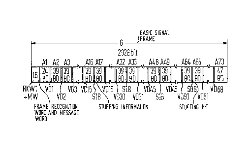
FIG. 3 illustrates a basic frame G comprising 2928
bits for the 139, 264 kbit/s signal. It contains sections
Al---A73 of which the sections Al--A72 each contain 40 bits
and the section A73 comprises 48 bits. The section Al contains
a 12-bit frame recognition word RKWl at the beginning and a
4-bit message word MW, and subsequently, 24 bits of video data
BD. The multiple frame data VDl--VD68, three times the
stuffing information of the video signal SIB and one-time a
stu-ffable bit SBB of the video signal Dla are respectively
inserted in the first time slot in the sections A2--A73. A
further 39 bits of video data BD are inserted into the sections
A2--~72 and 40 bits of video data BD are inserted into this
section A73.
FIG. 4 illustrates a multiplexer for use in
practicing the present invention. The multiplexer comprises
an input 1 in the form of a 10-bit bus for the video signal Dla,
a clock adapter 2 comprising an elastic memory 3 and a phas~
comparator 4, a 10-bit bus 7, a pair of parallel-to-series
converters 8 and 10, a pair of multiplexers 14 and 20 r a
central clock 24, a binary/CMI converter 28, a base generator
2g and an oukput 30.
A video signal Dla is received via the input 1,
being written in with the write-in clock tE having a frequency
13.5 MHz at an input 5. It is read from the elastic memory 3
at the kerminal 6 with a read clock tA which is supplied by
the central clock 24 which, in turn, receives a filling bit
information from the phase comparator 4 via the kerminal 59.
The clock adapted video signal Dla, together with a 6-bik frame
recognition word RKW2 at the terminal 9, is converted with
the video frame B of FIG. 1 and is inpuk into khe multiplexer
20 by way of the terminal 21 of the parallel-to-series converter
8. An 8-blt frame recognition word RKW3 for the multiple frame,
as well as the second through fourth digital signal D2a through
D4a are ~put into the multiplexer 14 via the terminals 15--
18, the multiplexer 14 feeding the mulkiple frame data VDl--
VD68 into the parallel-to-series converter 10 via the terrninal
13. A 12-bit frame recognition word RKWl and a Eour-bit
message word MW of the basic frame G are also input into the
parallel-to-series converter 10 via the terminals 11 and 12.
The sum signal proceeds via the terminal 22 ko the multiplexer
20 which emits the 139, 264 kbit/s signal having the basic
frame G of FIG. 3 at its oukput 26. The binary/CMI converter
28 converts the signal into the CMI line code which is
transmitted onto the line via the output 30.
A 139, 264 kHz clock is generaked in the base
generator 29, this clock being inpuk into the central clock
24 via the terminal 27, the clock 24, in turn, controlling
the multiplexer 14 via the terminal 19, the clock adapter 2
via the terminal 6, the parallel-to-series converters 8 and
10 via the terminal 25, and the multiplexer 20 via the
-- 10 --
z~
terminal 23. The known apparatus for stuffing have been
omitted for the sake of clarity.
The video signal Dla at the input 1 was acquired
in a 9-bit analog/digital converter after a low-pass
filtration and was converted into 10-bit code words in an
error protection circuit.
FIG. 5 illustrates a demultiplexer which may be
employed in practicing the present invention. The demultiplexer
comprises an input 31, a series-to-parallel converter 32, a
four-bit bus connection 34, a synchronizing device 35 which
interprets the 16-bit frame recognition word RKWl and the
four-bit message word MW, a second four-bit bus connection 36,
a demultiplexer 39 for the video signal Dlb, a pair of
10-bit buses 49 and 56, a clock adapter 50, a clock supply 42,
and a demultiplexer 44. The clock adapter 50 comprises an
elastic memory 51, a voltage-controlled oscillator 52 and a
phase comparator 54. A CM~/binary converter re~uired at the
input side and a device for deriving the 139, 264 kHz clock
are not shown.
A 139, 264 kbit/s signal D5b is applied to the input
21 and is converted in the series-to-parallel converter 32
into a parallel 4-bit code word with a bit rate of 34,816 kbit/s.
After a recognized 12-bit frame recognition word RKWl, a
synchronization signal is output in the synchronizing device
35, a commercially availa~le integrated circuit SH100-B-864,
being output to the central clock 42 via the terminal 38. The
four-bit message word MW is also gated out. Th~ position of
the multiple frame data VDl--VD68 is obtained after a first
position of every 10th four-bit code word and are supplied to
the demultiplexer 44 having a standard buffer memory,
destuffing device and monitoring circuit. The second through
fourth digital signals D2b through D4b are available as
uniform data streams at the outputs 46-48. The video data
stream, as shall be set forth in greater detail with reference
to FIG. 6, is converted, in a series-to-parallel manner, in
the demultiplexer 39 into 10-bit code words, is destuffed and
is read via the elastic memory 51 ~ith a uniform 13.5 MHz
clock. The reading clock tA~ as usual, is acquired via the
phase comparison circuit 54 with the writing clock tEI being
acquired ~rom a voltage-controlled oscillator 52 which is
synchronized thereto. The clock supply 42 is controlled by
the incoming 139, 264 kHz clock at the input 57 and generates
all necessary clocks at the terminals 33, 37, 40, 43 and 58.
The clock adapters 2 and 50 are known from FIG. 7 of
the aforementioned article from the publication "telcom report",
and the apparatus described therein.
The apparatus for implementing the stuffing
procedure were not incorporated in FIG. 5 since they are well
known to those of ordinary skill in the art.
Referring to FIG. 6, a demultiplexer 39 of FIG. 5
is illustrated in detail. The demultiplexer comprises a
parallel-to-series converter 59, a 10-bit bus 61, a comparator
62 (an ECL F 100166 circuit), a setting device 63 for the
frame recognition word RKW2, and 10 D flip-flops in the form
of two series-connected integrated circuits, ECL F 100151).
The parallel-to-series converter 59 can be part of the
integrated circuit employed for the synchronizing device 35.
- 12 -
The four-bit code words applied to the input of the
demultiplexer 39 and, therefore, to the input of the parallel-
to-series converter 59 are converted into a 139,264 kbit/s
signal in the converter, this signal being, in turn,
converted in the series-to-parallel converter 60 into constantly
asynchronously traversing 10-bit code words. These code words
proceed via the 10-bit bus 61 to the comparator 62 which
constantly compares the same to a reference frame recognition
word RKW2a which is stored in the setting device 63. When the
frame recognition word RKW2 is recognized, a synchronizing
signal for the video frame is output at the output 41. The
10-bit codes are also supplied via the 10-bit bus 61 to the
ten D flip-flops 64 whose outputs form the output cf the
demultiplexer 39. The frame recognition word RKW2 is thereby
gated out with the assistance of the clock at the clock input
40.
Although we have described our invention by reference
to a particular illustrative embodiment thereof, many changes
and modifications of the invention may become apparent to
those skilled in the art without departing from the spirit and
scope of the invention. I therefore intend to include within
the patent warranted hereon all such changes and modifications
as may reasonably and properly be included within the scope of
our contribution to the art.