Note: Descriptions are shown in the official language in which they were submitted.
INTRINSICALLY SAFE BATTERY CIRCUIT
Backqround of the Invention
1. Field of the Invention
The present invention relates generally to overload
protection circuits, but more particularly to a bat~ery
protection circuit for portable radios used in ha2ardous
environments.
20 Description of the Prior Art
Overload protection devices, such as fuses, series
current limiters, and electronic crowbar circuitsV are
well known and widely used in the art. Of these prior
devices, few are applicable for use in hazardous
environments--locations in which the atmosphere contains
gas, vapor, or dust particles which could easily be
ignited by sparks or thermal heating. A fuse, for
example, poses a thermal ignition threat under overload
conditions. Similarly, current limiting circuits
generally allow a maximum load current to flow under
fault conditions. Although the current shutback feature
of a crowbar circuit is desirable, these devices exhibit
a slow response time allowing ~he possibility that sparks
will be produced.
Even fewer prior art overload protection circuits
accommodate the specific problems of battery operated
~"
:~,
,
. .
, . ~ ~'i .
~ .
,
,
' : . ,
:- :
equipment such as portable two-way radios. Portable
applications present the additional requirements of low
power consumption during uSe; negligible power
consumption when not in use; and minimal voltage drop
across the battery protection circuit. Furthermore,
portable applications introduce severe size and cost
limitations such that the protection circuit can be built
inside each individual battery housing.
Bogut, in U.S. Patent No. 3,686,530, entitled
"Current Limited Battery Pack~" presents an example of a
battery protection circuit incorporated into the battery
housing. Bogut controls a series transistor or relay by
sensing excessive current through a series resistor to
fire a silicon-controlled rectifier (SCR).
Unfortunately, equipment specifications for certain types
of hazardous atmospheres require either continuous
current limiting capability, or a faster response time
than this technique is capable of producing.
Furthermore, the Darlington transistor pair exhibits a
substantial voltage drop.
A need, therefore, exists for an intrinsically safe
battery protection circuit that meets the stringent
specifications for use in explosive atmospheres while at
the same time being compatible with the requirements of
portable radio applications.
Summary of the Invention
Accordingly, it is an object of the present
invention to provide an intrinsically safe battery
circuit for portable radio applications for use in
hazardous atmosphere environments.
A more particular object o the present invention is
to provide a battery protection circuit which exhibits
negligible power consumption when not in use.
Another object of the present invention is to
provide a battery protection circuit exhibiting minimized
power consumption during use.
Still another object of this invention is to provide
a battery protection circuit exhibiting low series
voltage drop.
In practicing the invention, an overload protection
circuit is provided for limiting the current supplied by
the batt~ry to a load. The circuit is particularly
adapted for use in por~able radio applications which must
meet rigorous specifications of intrinsic~ safe
equipment for use in hazardous environments. The
protection circuitry includes: a load sensor circuit
adapted to detect when the load is turned on which then
powers up the remaining protection circuitry, thus
presenting negligible current drain from the battery
under no load conditions; a current sensor/current
trip/current limit mechanism which controls the amount of
energy delivered to the load such that sparking or
thermal heating is prevented; and a voltage trip circuit
to detect when load current is below the current trip
level under low battery voltage conditions, thus
preventing overdissipation of the power switch device.
Furthermore, the present invention provides a simple,
inexpen~ive, compact circuit capable of being
incorporated inside the battery housing to accommodate
portable radio applications.
R ~t~ p~
Brlef Descri~tion of the Drawings:
The features of the present invention which are
believed to be novel are set $orth with particularity in
the appended claims. The invention itself, however,
together with further objects and advantages thereof, may
best be understood by reference to the following
description when taken in conjunction with the
accompanying drawings, in which:
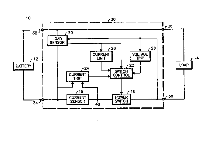
Figure 1 is a block diagram illustrating the
preferred embodiment of the intrinsically safe battery
circuit of the present invention; and
Figure 2 is a schematic representation of the
preferred embodiment of Figure 1 illustrating the
individual components of the battery protection circuit.
Detailed Description
Referring now to the drawings, Figure 1 is a block
diagram of intrinsically safe battery circuit 30 having
input terminals 32, 34 and output terminals 36, 38 such
that circuit 30 is connected between battery 12 and load
14~ The battery protection circuit serves to limit the
amount of energy supplied to a load such that, in the
event of a short circuit, sparking or thermal heating is
prevented. Furthermore, intrinsically safe battery
circuit 30 presents negligible current drain when the
load is disconnected, such that the battery will not be
discharged.
,. -
, ' . , ~ ':
:, ~, ..
Load sensor 20, connected between input terminals 32and 34, continuously monitors for the presence of a load
at output terminals 36 and 38. When no load is present
~i.e., when the portable radio is switched off), load
sensor 20 sign~ls switch control 22 to disable power
switch 16 such that a continuous current path from
battery 12 to load 14 does not exist. When load 14 i5
switched on, battery voltage from terminal 36 is applied
through the load to terminal 38 and and to load sensor
20. 1Oad sensor 20 then detects the presence o the load
and signals switch control 22 to enable power switch 16.
Thus~ a return current path to the battery is provided
from terminal 38 through power switch 16 through current
sensor 18 to terminal 34.
The current control mechanism consists of current
sensor 18, current trip circuit 24, and current limit
circuit 26. Current trip circuit 24 monitors the voltage
developed across current sensor 18 to provide a disable
signal to switch control 22 in the event of an overload
conditlon. Switch control 22 then disables power switch
16 such that no current is available to prevent thermal
heating in the load. Power switch 16 will remain
disabled until the load is completely removed. Current
limit circuit 26 senses the amount of drive signal
applied to switch control 22 from load sensor 20 to
provide a maximum switch control signal level which
limits the drive to power switch 16. As a result,
current limit circuit 26 continuously limits the maximum
load current through power switch 16.
Under low battery voltage conditions, the
possibility exists that switch control 22 would not
provide enough drive signal level to fully saturate power
switch 16. If this occurs, during periods of high load
current ~but less than a predetermined current trip
_5_
:
'`, .
.: .
. ,~.
point~, then power switch 16 could overdissipate.
Voltage trip circuit 28 prevents this low voltage/high
current condition from occurring~ When power switch 16
comes out of saturation, terminal 38 voltage increases.
Vol~age trip circuit 28 continuously monitors terminal 38
to provide a voltage trip signal to switch control 72 to
disable power swi~ch 16 before overdissipation occurs.
Power switch 16 remains disabled until the load is
removed~
In review, intrinsically safe battery circuit 30
limits the amount of battery output current applied to a
load such that hazardous gases will nvt be ignl~ed by
sparks or thermal hea~ing during short circuit
conditions~ Load sensor 20 enables the remaining
circuitry only in the presence of a load, providing the
significant advantage of negligible battery drain under
no-load conditions. Current sensor 18/current trip
circuit 24/current limit circuit 26 provides a mechanism
to prevent hiyh currents from causing sparks or thermal
heating. Voltage trip circuit 28 prevents
overdissipation of power switch 16 under low battery
voltage conditionsr
Figure 2 illustrates the components of the preferred
embodiment of intrinsically safe battery circuit 30.
Positive battery voltage is applied to input terminal 32,
and nega~ive voltage is applied to input terminal 34
which is ground. Similarly, an external load is
connected across output terminals 36 and 38. One
important feature of the present invention i5 that load
voltage is sensed at terminal 38, alleviating the
requirement for an external voltage sensing terminal.
Load sensor 20 is comprised of PNP transistor Q3,
NPN ~ransistor Q4, and associated resistors and
~'
.
.:
: : :
.... . :
`
,
. . .
.d ~ b
capacitors~ This load sensor circuitry receives battery
voltage from terminal 32 and ground at terminal 34. When
the external load is disconnected, terminal 38 is at
ground potential, and transistors Q3 and Q4 are cut off.
Power switch 16 is comprised of MOSFET transistor Ql
coupled in series between input terminal 34 and output
terminal 38. This power switch device remains in a
nonconductive state when no load is present. A MOSFET
transistor has extremely high input impedance as compared
to a bipolar transistor. The use of MOSFET transistor Ql
as power switch 16 permits the battery protection circuit
to control high drain-source currents without requiring
high gate currents. If a bipolar transistor switch were
used, substantial base current would be wasted during
periods of high load currents. Thus, the present
technique of implementing a MOSFET switch provides an
important power savings for portable applications.
Switch control circuitry 22 includes resi~tor R6,
resistor R12, capacitor Cl, capacitor C19, and
silicon-controlled rectifier SCR27 These resistors
couple control signals to the gate of transistor Ql.
~; Capacitor Cl and capacitor Cl9 function as RF bypasses.
SCR2 provides the mechanism to disable transistor Ql in
response to a current trip signal or a voltage trip
signal.
Current sensor 18 is comprised solely of resistor 13
conne-cted in series between input terminal 34 and the
source terminal of transistor Ql. Under overload
conditionsr excessive load currents develop a voltage
across R13. This voltage is monitored by current trip
circuit 24, which, in turn, provides a disable signal to
switch control 22.
; Current trip circuitry 24 is comprised of:
; resistors R9, R10, and R15; capacitors C5, C6, and C21,
~ -7-
:,
.
, .
. .- '' ' ~ ' ' ~' ' `' :
.
.
R ~
hot carrier diode CR2, and temperature sensitive resistor
(thermistor) RT2. This temperature compensated bias
circuitry allows R13 to be a smaller value than if the
SCR were directly fired by the voltage across R13. C5
and C21 function 25 RF bypasses. Capacitor C6 introduces
a time delay at ~he gate of SCR2 to prevent current
and/or voltage tripping during initial turn-on of the
radio.
Current limiting is provided by zener diode CR4
coupled to the gate of transistor Ql. The voltage ~rip
function is performed by resistor R17, which ~onitors the
load voltage at terminal 38 to apply a voltage trip
signal to SCR2.
Briefly, intrinsically safe battery circuit 30
operates as follows:
A. No-load Conditions.
Under no-load conditions, transistor Ql is off,
output terminal 38 is at ground potential, and
transistors Q3 and Q4 remain off. Thus, the only current
drain from the battery is that of collector-emitter
leakage currents of transistors Q3 and Q4. This feature
of negligible current drain (i.e., less than 1 microamp)
under no-load conditions can be a significant advantage
in portable radio applications since the battery will not
become discharged when the radio is not being used.
-
B. Turn-on.
When an external load is connected (i.e., the radio
is turned on), the voltage at terminal 3a rises to
approximately battery potential. This voltage is applied
to the junction of R4 and R5 providing base current for
:, ,~ ' .
;, ' '`' ` ' ~
,
:-;: '
transistor Q4. Q4 then turns on and provides base
cu~rent for transistor Q3 through resistor R2
Transistor Q3 turns on and applies its collector voltage
to the gate of power switch transistor Ql through series
resistors R6 and R12. Now transistor Ql conducts,
reducing the voltage at terminal 38 to approximately 0.6
volts (with respect to ground). Transistor Q4 remains on
as long as Q3 supplies supplementary base current through
resistor R3 and as long as 0.5 volts remains at the drain
terminal of Ql. Transistors Ql, Q4, and Q3 for~ a closed
loop ~o maintain a constant 0.6 volts output at terminal
38. Capacitor C12 provides damping for the loop.
If the load current increases (i.e., under radio
transmit conditions), the voltaqe across the drain to
source of Ql will increase. This slight incrëase in
drain voltage will turn Q4 on harder, which will then
turn Q3 on harder, such that a higher gate voltage is
applied to Ql. Consequently, the drain-to-source
impedance of transistor Ql will decrease such that
approximately 0.6 volts i5 maintained at terminal 38.
C. Turn-off.
When the external load is disconnected, the voltage
at output terminal 38 falls ~o zero. Consequently,
transistor Q4 receives insufficient base current through
resistor R4 to stay on. When Q4 turns off, Q3 then turns
off which shuts down the voItage ~upply to the rest of
the circuit. With zero gate voltage, transistor Ql turns
off and battery current drops to approximate1y ~ero.
,:
_g_
~ , .
,
, :
D. Current Limiting.
Zener diode CR4 coupled to the gate of transistor Ql
functions as a cuxrent limiter. As the load current
increases, the closed loop combination of transistors Ql,
Q3, and Q4 track this current increase and compensate by
increasing the voltage at the gate of transistor Q1. If,
however, the load current approaches a predetermined
maximum level (i.e., 5 amps), then 2ener diode C~4 clamps
the voltage at the junction of resistors R6 and R12 to a
maximum gate voltage which corresponds to this maximum
current level. Any load current demands beyond this
maximum current level will not be met by an increase in
gate voltage of Ql. As a result, 2ener diode CR~ sets a
minimum drain-to-source resistance of MOSFET transistor
Ql which results in a maximum current level during
overload conditions.
This method of monitoring the gate voltage of a
MOSFET transistor provides continuous current limiting
for the battery protection circuit. For a more precise
current limit threshold, the zener diode's breakdown
voltage may be selected to match the particular MOSFET's
gate pinch-off voltage.
E. Current Tripping
In addition to current limiting, it is desirable to
provide a current trip mechanism such that no current
flows through a short circuit to protect against thermal
heating. Current sensor 18 in combination with current
trip circuit 24 provide this function. Current sensor 18
consists solely of series resistor R13 coupled in the
load curren~ return path. When excessive load current
flows, a substantial voltage is developed across R13.
-ln-
,
.
. . .
,
- : :
r-~
Current trip circuit 24 mo~itors this series voltage drop
and provides a disable signal to SCR2 of switch control
circuit 22.
The gate of SCR2 is biased at about 0.3 volts with
respect to the source terminal of transistor Ql by the
combination of resistor R9, R10, R15, thermistor RT2 and
hot carrier diode CR2. Under normal load current
conditions, diode CR2 holds the gate voltage of SCR2 at
0.3 volts, which is below its Q~5 volts firing thre~hold.
If the external load current exceeds a predetermined
level, then the voltage developed across R13 will
increase until the SCR gate trigger level of 0.5 volts is
reached, firin~ the SCR. When the SCR conducts~ ~he gate
voltage of Ql is pulled low to approximately 1 volt~
This turns Q1 off. Thus, the battery is effectively
disconnected from the load. The battery circuit will
stay in this disconnected state until the external load
is completely removed. When the load is removed,
transistors Q3 and Q4 will turn off to reduce the SCR
anode-to--cathode current to zero. Thus, the battery
protection circuit of the present invention resets itself
when the external load is disconnected.
The SCR gate biasing arrangement of the present
invention allows the value of current sensor resistor R13
to be minimized--a significant advantage in portable
applications. If a typical SCR gate biasing arrangement
were used, a current trip level of 2.0 amps, for example,
would require R13 to be 0.25 ohms to develop the G.5
volts required to fire SCR2. However, since the gate of
SCR2 is nominally biased at 0.3 volts with respect to its
cathode by hot carrier diode CR2, only 0.2 volts
developed across R13 is required to fire the SCR. Using
the same current trip level of 2.0 amps, R13 can now be
:.-
~ ,
.
reduced to 0.1 ohm. Thereforel the voltage drop inseries with the external load is kept to a minimum.
Thermistor RT2 is required for temperature compensation~
since the hot carrier diode junction does not track the
SCR gate junction over temperature. Thi~ SCR biasing
technique provides the significant advantage of reducing
the series voltage drop of the battery protection
circuit.
F. Voltage Tripping.
When the battery becomes discharged, the voltage
applied to the gate of Ql is correspondingly reducedO If
this reduced gate voltage is insufficient to saturate Ql,
then the transistor may dissipate a significant amount of
power under high current conditions. To prevent
overdissipation (and a possible explosion in a hazardous
environment), voltage trip circuit 28 turns off Ql before
it is damaged due to excessive heating.
Resistor R17 senses an increase in voltage at the
drain of Ql to apply a voltage trip signal to the gate
terminal of SCR2. When a sufficiently high drain voltage
is reached, the SCR fires and turns Ql off by clamping
its gate voltage ta approximately 1 volt. The SCR
remains in a conductive state until the load is
disconnected. Capacitor C6, connected to the gate of
SCR2, provides the necessary time delay to prevent
voltage or current tripping upon initial radio turn-on.
ln summary, an intrinsically safe battery circuit
has been described which limits the amount of current
supplied by the battery to a load. The circuit is
particularly well adapted for use in portable radio
applications in which the equipment used must meet strict
.~
:, .
~ -12-
.~
: ~
,
, , : .
, ~,
` '
~d,,~?e,l 9r~f`~
specifications of hazardous atmosphere environments. The
bat~ery protection circuit of the present invention
provides the following advantages: negligible power
consumption when not in use; minimized power consumption
during use; continuous current limiting, overcurrent trip
protection; switch device overdissipation protection;
minimal series voltage drop; and inexpensive~ compact
circuit configuration.
While spesific embodiments of the present invention
have be@n shown and described herein, further
modifications and improvements may be made by those
skilled in the art. All such modifications which retain
the basic underlying principles disclosed and claimed
herein are within the scope of this invention.
What is claimed is:
-13-
. .
~ .
~.