Note: Descriptions are shown in the official language in which they were submitted.
--1--
.
AN ll\~PROVED THERMAL INK JET PRINTlIE~D
BACKGROU~D OF T IE INVENTION
5 Field of the Invention
This invention relates to thermal ink jet printing, and more
particularly to an improved thermal ink jet printhead.
Description of the Prior_Art
10Generally, a drop-on-demand, ink jet printing system has a
printhead that uses thermal energy to produce a vapor bubble in an ink-filled
channel in order to expel a droplet. This type of printing is referred to as
thermal ink jet printing or bubble ink jet printing and is the subject matter o~the present invention. In existing thermal ink jet printing, the printhead
15comprises one or more ink filled channels? such as disclosed in IJ.S. 4,463,359
to Ayata et al, communicating with a relatively small ink supply chamber at
one end and having an opening at the opposite end, referred to as a nozzle. A
thermal energy generator, usually a resistor, is located in the channels near
the nozzles a predetermined distance therefrom. The resistors are individually
20 addressed with a current pulse to momentarily vaporize the ink and form a
bubble which expels an ink droplet. As the bubble grows, the ink bulges from
the nozzle and is contained by the surface tension of the ink as a meniscus. As
the bubble begins to collapse, the ink still in the channel between the nozzle
and bubble starts to move towards the collapsing bubble, causing a volumetric
25 contraction of the ink at the nozzle and resulting in the separation of the
bulging ink as a droplet. The acceleration of the ink out of the nozzle while
the bubble is growing provides the momentum and velocity of the droplet in a
substantially straight line direction towards a recording medium, such as
paper.
31)The printhead of IJ.S. ~,~63,359 has one or more ink-filled channels
which are replenished by capillary action. A meniscus is formed at each
nozzle to prevent ink from weeping therefrom. A resistor or heater is located
in each channel upstream from~ the nozzles. Current pulses representative of
data signals are applied to the resistors to momentarily vaporize the ink in
35 contact therewith and form a bubble ~or each current pulse. Inlc droplets areexpelled from each nozzle by~ the growth of the bubbles which causes a
: ~
, ~
:
......
,,
, I' .
: ' ~ : : -: , ,:
quantity of ink to bulge from the nozzle and break off into a droplet at the
beginning of the bubble collapse. The current pulses are shaped to prevent the
meniscus from breaking up and receding too far into the channels, after each
droplet is expelled. Various embodiments of linear arrays of thermal ink jet
devices are shown such as those having staggered linear arrays attached to the
top and bottom of a heat sinking substrate and those having different colored
inks for multicolored printing. In one embodiment, a resistor is located in the
center of a relatively short channel having nozzles at both ends thereof.
Another passageway is connected to the open-ended channel and is
10 perpendicular thereto to form a T-shaped structure. Ink is replenished to theopen-ended channel from passageway by capillary action. Thus, when a bubble
is formed in the open-ended channel, two different recording mediums rmay be
printed simultaneously.
U.S. 4,275,290 to Cielo et al discloses a thermally activated liquid
lS ink printing head having a plurality of orifices in a horizontal wall of an ink
reservoir. In operation, an electric current pulse heats selected resistors thatsurround each orifice and vaporizes the non-conductive ink. The vapor
condenses on a recording medium, such as paper, spaced above and paraLlel to
the reservoir wall, causing a dark or colored spot representative of a picture
20 element or pixel. Alternatively, the ink may be forced above the orifice by
partial vaporization of the ink, so that the ink is transported by a pressure
force provided by vapor bubbles. Instead of partially or completely vaporizing
the ink, it can be caused to flow out of the orifices by reduction of the surface
tension of the ink. By heating the ink in the orifices, the surface tension
25 coefficient decreases and the meniscus curvature increases, eventually
reaching the paper surface and printing a spot. A vibrator can be mounted in
the reservoir to apply a fluctuating pressure to the ink. The current pulse to
the resistors are coincident with the maximum pressure produced by the
vibration.
U.S. 4,438,191 to ~loutier et al discloses a method of making a
monolithic bubble-driven ink jet printhead which eliminates the need for using
adhesives to construct multiple part assemblies. The method provides a
layered structure which can be manufactured by standard integrated circuit
and printed circuit processing techniques. Basically, the substrate with the
35 bubble generating resistors and individually addressing electrodes have the inlc
chambers and nozzles integrally formed thereon by standard semiconductor
...
'~
;
A~ ~$ ~
--3--
processing.
U.S. Re-issue Patent RE 32572 to Hawkins et
al, discloses a thermal ink jet printhead and
method of fabricQtion. In this CQSe, a plurality of printheads m~y be
concurrently fabricated by gorming a plurality of sets of heflting elements withtheir individual addressing electrodes on one silicon wafer and etching
corresponding sets of grooves which may serve as ink channels with a common
reservoir in another silicon wafer. The two wafers are ~ligned and bonded
together, so that each channel has a heating elernent and then the indiYidual
printheads are obtained by milling aw~y the unwant~d silicon materi~l to
expose the Qddressing electrode termin~ls and then dicing the waf~r into
separate printheads.
In all bubble jet or thermal printheads, it is important to be able to
keep the ink droplet velocities relatively high and to impart a large momentum
to the ejected droplet. This is so, for example, to minimize misdirectionality
of the drople$ caused by wetting effects at the channel orifices or nozzles and
to help ovecome first droplet ejection problems in order to assure stable,
uniform printing. High droplet velocities and large impulses may be attained
by placing the heating element nearer the orifice, so that only a small amount
of ink is acted upon by the bubble growth and collapse and/or ~y increasing the
heating element current pulse duration to generate more thermal energy,
thereby increasing the amount of stored heat in the ink prior to nucleation of
the micro-sized vapor bubbles which will lead to a more rapid or explosive
bubble growth.
However, in the typical bubble jet printhead d~scussed above and
shown in Figure 3a, application of one or both of these methods is very limited
due to the phenomenon referred to as "blowout." "Blowout" is the mechanism
by which a growing bubble within a printhead channel can expand so far as to
push out past the channel orifice and release some of the vapori2ed ink. This
occurrence can lead to the ingestion of air into the channel and the possibilityof a large trapped air bubble over the heating element surface, as well as a
misdirected, weakly propelled droplet. Ar,y trapped air bubble will seriously
affect the nucleation process in the ink over the heating elment's surfaee, as is
well known in the ~rt, and cause subsequent misfirings from that channel. This
blowout of the growing bubble is due to the lateral spreading of the bubble as
it grows. Therefore, placement of the he~t;ng element eloser to the orifice
~A .
- . ,
- , -, . . - . .
". ,
.. .
- , .. . , , ~ -
.: ~ , ., . . .. , ~ .
'' :
and/or increasing the heating pulse duration make blowout more likely. Thus,
prior art devices accept the lower droplet speeds from less explosive bubble
growth to avoid the blowout phenomenon.
SUMM~RY OF T~E INVENTION
It is an object of the present invention to provide an improved ink
jet printhead for high resolution printing that is more operationally efficient.It is another object of this invention to provide an improved
thermal ink jet printhead which prevents lthe blowout of vaporized ink from
the bubble produced thereill to expel a droplet therefrom.
It is still another obje~t of this invention to provide an improved
thermal ink jet printhead capable of increased heating element pulse durations
to overcome first droplet problems and to produce higher velocity for the
emitted droplets.
It is yet another object of this invention to enable placement of the
heating elements ~loser to the printhead nozzles thereby providing further
means for keeping the velocities of the emitted droplets high.
It is still a further object of this invention to provide an improved
printhead capable of increased operating droplet emitting frequencies, since
the increased duty cycles per heating element leading $o an inerease in the
operational temperature of the ink caused thereby are not as likely to produce
vapor blowout.
It is an additionai object of the invention to provide ~ printhead
having each of the bubble generating heating elements positioned at the
bottom of a recess in the channels, the recesses being located a predetermined
distance upstream of the channel nozzles.
In the present invention, each bubble generating heating element of
- the improved thermal ink jet printhead is placed in the bottom of a recess of
predetermined depth in one wall of each channel a predetermined distance
upstream of the channel nozzles, so that the sides ol the vapor bubbles
produced are constrained by the recess walls from moving along the ink flow
path and out of the nozzle and instead made to grow in a direction normal to
the recess bottom. Such an arrangement avoids the occurrence of vapor
blowout as experienced by prior art devices when irmproved performance is
sought fr~m the prior art printheads.
:
~ , - .
~:- - ,' ~ ~ -
,
In fact, the latitudes for the heating element
pulse duration and the heating elament placement in the
channel relative to the channel no~zle are both increased
when the recessed heating element concept i6 u6ed. Thus,
longer heating element pulses may be applied, and the
ehating element may be closer to the nozzle before
blowout of vapor occurs and becomes a problem.
According to a broad aspect, the invention
relates to a thermal ink jet printhsad for e~ecting and
-~ropelling ink droplets on demancl therefrom along a
flight path from orifices in the printhead toward a
recording medium spaced therefrom by momentarily heating
ink located in straight aapillary channels within the
printhead that interconnect respective ones of the
orifices with an ink supplying reservoir also within the
printhead, the channels and orifices having ubstantially
equal aross-sectional areas, thus forming a straight ink
flow path therebetween to produce temporary vapor bubbles
in the channels, the heating of the ink being in response
to electrical input signals representing digitized
ignals 6electively applied to individual heating
elements located one each in the channels adjacent the
orifices, the printhead comprising: an upper substrate
having first and ~scond parallel surfaces and two
opposing, parallel edge faces that are perpendicular to
the subst~ate ~urfaces, the first surface containing a
depression and a plurality of parallel straight grooves,
one end of the grooves perpendicularly penetrating one
upper substrate faae and the other ends of the grooves
opening into the depression; a lower substrate having
first and second parallel surfaces and an edge face
perpendicular to the lower substrate surface~, a
plurality of heating elements having urfaces with
predetermined arsas and being formed in a row on the
lower substrate first sur ace parall~l with and a
predetermined distance from the lower substrate face,
together with respective electrode~ for s21ectively
::
:
, :
~. ~
3~3
- 5a -
addres~ing the heating elements with said electrical
input signals, the addressing electrodes having terminal
ends at the edges of the lower substrate fir6t surface
other than the one adjacent its edge faoe; a passivation
layer covering the lower substrate first surface,
including said addressiny electrodes, but excluding the
heating element surfaces and the terminal ends of the
addressing electrodes, these having been cleared of the
passivation layer; a thick film i.nsulative layer having a
predetermined thickne~ 8 overlaying only the passivation
layer, so that the thic~ness of the thiak film layer
provide~ substantially perpendicular walls that
individually surround each of the heating elements, thus
placing each heating element surface at the bottom of a
recess produced by said thick film walls; said upper and
lower substrate being aligned and bonded together to form
the printhead with their respectiYe first sur~aces being
confrontingly joined and with the upper substrate face
having the groo~e penetrations being coplanar wi_h the
lower substrate face, ~o that the upper æubstrate
depression and grooves respectively become the ink
reservoir and the ink channels, the groove penetrations
in the upper substrate face become the orifices, the
alignment of the upper and lower substrates places one
recessed heating element in each channel a predetermined
distance from an associated orifice, ~o that the thick
film walls inhibit the growth of the vapor bubbles in a
direction parallel with the ink flow path in 6aid
channels while promoting bubble growth in a direction
normal to the heating elements, whereby the heating
element reoess in said thick film layer enables closer
placement of the heating element~ to the orifices and the
consequent e~ection of higher velocity droplet and yet
prevents vaporized ink blowout during 8 aid droplet
: : .
-
,
.:
,",.;. :, .",
- 5b -
ejecting bubble generation; means for connecting the
printhead reservoir to a 60urce of ink under a
predetermined pressure external to the printhead; and
means for addressing the electrode terminal ends with
said input ~ignals.
According to a further broad aspect, the invention
relates to an improved thermal ink jet recording
apparatus for ejecting and propelling ink droplets on
demand along a flight path towarcl a recording medium
spaced therefrom in respon~e to electrical input signals
representing digitized data 6ignals ap~lied thereto,
comprising: at least one elongated, straight channel
defining a straight ink flow path therethrough with
substantially uniform cross-sectional area and having an
orifice on one end substantially perpendicular to the ink
flow path, the other end 6erving as an inlet in
communication with an ink reservoir; means for fi1ling
and maintaining the reservoir and channel with ink having
a predetermined preasure, the channel and orifice being
of substantially equal cros~-~ectlonal area and
dimensioned to cause a meniscu6 to be ~ormed at the
orifice that has a suxface tension which prevents ink
from weeping therefrom; a heating element being located
internally of the channel and having a surface with a
predetermined surface area contacting the ink, the
surface of the heating element being perpendicular to the
ink flow path in the channel, the heating element æurface
being positioned at the bottom of a recess having a
uniform depth in the range of 10 to 100 microns in a
surface portion of the channel, 6aid rece s having walls
that closely surround the heating element and that are
substantially perpendicular thereto, ~aid recess being
po~itioned closely adjacent and upstream of 6aid oriflce
for a distance of about 2 to 3 mils or S0 to 75 microns;
,, ,
. .
L~
- 5c -
means for applying current pulses to the heating element
in said recess in response to the input 6ignals, the
pulses each having ~ufficient amplitude and duration to
vaporize momentarily the ink contacting the heating
element surface substantially instantaneously to ~orm a
temporary vapor bubble which causes the expul6ion of a
discrete droplet of ink from saicl orifice in a direation
in substantial alignment with the ink flow path in 6aid
straight channel and propels it 1:owards the recording
medium, the walls of the recess containing khs heatiny
element inhibit.ing the ~rowth of the bubble in a
direction parallel to said ink flow path and 6ald surface
of the heating element, while promoting bubble growth in
a direction normal to the surfaae of the heating element,
and thus enabling closer location of the heating element
to the orifice and the consequent ejection oE higher
velocity droplets while preventing a release o vaporized
ink from the bubble during the droplet expulsion with a
consequent ingestion of air, so that the opsrational
efficiency of the pxinthead is improved; and the ink from
the reservoir replenishing the ink in the channel by
capillary action each time a droplet is expelled.
-
~ :. :, ::,, . ., . :, - .
:. :.-.
, ~ . . .
., ,~: , ~: , . .
- 5d -
RIEF DESCRIPTION OF THE DRAWINGS
Figure 1 is a schernatic isometric view of a carriage type thermal
ink jet printing system incorporating the present invention.
Figure 2 is Q plan view of the daughter board and fixedly mounted
printhead showing the terminals of th~e printhead electrodes wire-bonded
electrodes to one end of the electrodes of the daughter board.
Figure 3a is an enlarged sche~matic cross-sectional side view of a
prior art printhead channel depicting the occurrence of a vapor blowout.
Figure 3b is an enlarged schematic cross-sectional side view of a
printhead channel showing the recessed heating element of the present
invention preventing vapor blowout.
Figure 4.is an enlarged schematic isometric view of a prirlthead
mounted on the daughter board showing the ink droplet emitting nozzles.
Figure 5 is a schematic plan view of ~ wafer having a plurality of
heating element arrays and addressing electrodes, with one heating element
array and one alignment mark being shown enlarged.
Eigure 5a is an enlarged partially shown isometric view of the
heating element plate, partially sectioned to show the recessed heating
elements.
Figure 6 is a schematic plan view of a wafer having a plurality of
ink manifold recesses, with one manifold recess and one alignment openin~
being shown enlHrged.
Eigure 7 is an enlarged isometric view of one set of channels which
were later diced into one of the manifold recess walls of Figure 6.
Figure 8 is an enlarged cross-sectional view of the wafer of Figure
6 as viewed along the line "8-8" thereof, showing an alignment opening and a
recess which will later form the fill hole.
Figure 9 is a cross-sectional view of the enlarged manifold recess
of Figure 6 as viewed along line "9-9" thereof.
. ,,
. .
'. '~' ~
J~'~3~
Figure 10 shows an enlarged isometric view of the channel and
manifold wafer bonded to the wafer with the heating elements after the
excess channel wafer material has been removed.
S DESCRIPTION OF TH~ PREFERRED EIl~BODIMENT
,
A typical carriage type, multicolor, thermal ink jet printing device
10 is shown in Figure 1. A linear array of ink droplet producing channels is
housed in each printhead 11 of each ink supply cartridge 12 which may
optionally be disposable. One or more ink supply cartridges are replaceably
mounted on a reciprocating carriage assembly 14 which reciprocates back and
forth in the direction of arrow 13 on guide rails 15. The channels terminate
with orifices or nozzles aligned perpendicular to the carriage reciprocating
direction and parallel to the stepping direction of the recording medium 16,
such as paper. Thus, the printhead prints a swath of information on the
stationary recording medium as it moves in one direction. Prior to the
carriage and printhead reversing direction, the recording medium is stepped by
the printing device a distance equal to the printed swath in the direction of
arrow 17 and then the printhead moves in the opposite direction prillting
another swath of information. Droplets 18 are expelled and propelled to the
recording medium from the nozzles in response to digital data signals received
by the printing device controller (not shown), which in turn selectively
addresses the individual heating elements, located in the printhead channels a
predetermined distance from the nozzles, with a current pulse. The current
pulses passing through the printhead heating elements vaporize the ink
contacting the heating elements and produce temporary vapor bubbles to expel
droplets of inlc from the nozzles. Alternatively, several printheads may beaccurately ju ctapositioned to form a pagewidth array of nozzles. In this
configuration (not shown), the nozzles are stationary and the paper moves
therepast.
In Figure 1, several ink supply cartridges 12 and ficedly mounted
electrode boards or daughter boards 19 are shown in which each sandwich
therebetween a printhead tl, shown in dashed line. The printhead is
permanently attached to the daughter board and their respective electrodes
are wire-bonded together. A printhead fill hole, discussed more fully later, is
sealingly positioned against and coincident with an aperture (not shown) in the
cartridge, so that ink from the cartridge is continuously supplied to the ink
. ,.
- ~ :. . . . .~ :
- . ~.. . : ,
. . .
.. ..
~ 2~ J~
channels via the manifold during operation of the
printing device. This cartridge is similar to and more
fully described in U.S. Patent 4,571,599 to Rezanka.
Note that the lower portion 20 of each daughter
S board 19 has electrode terminals 21 which extend below the cartridge bottom
2a to facilitate plugging into a temale receptaele (not shown) in the carriage
assembly 14. In the preferred embodiment, the printhead contains 48 channels
on about 3 mil centers (75 microns) for printing with a resolution of 300 spots
per inch (spi). Such a high density of addressing electrodes a3 on each
10 daughter board is more conveniently h~ldled by having some of the electrodes
terminate on both sides. In Pigure 1, the side 24 shown is opposite the one
containing the printhead. The electrodes all originate on the side with the
printhead, but some pass through the dau~hter board. All of the electrodes 23
terminate at daughter board end 20.
A pl~n view of the L-sh~ped daughter board 19 is shown in Figure
2. This view is of the side containing the printhead 11. The daughter board
electrodes 23 are on a one-to-one ratio with the electrodes of the printhead
and are connected thereto by wire bonds 49. The printhead fill hole 25 is
readily ~pparent in this Figure 2. About half of the daughter board electrodes
2û 23, which are on the longer leg of the daughter board, sre on the opposite
surface thereof, so that both sides of the daughter board end portion 20 have
substantially identical parallel arrays of terminals 21. The electrodes on the
opposite side of the daughter board are electrically connected through the
daughter board at locations 26.
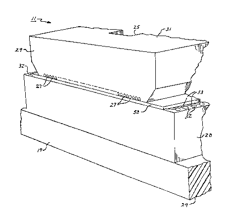
Figure 4 is an enlarged schemntic isometric view of the front face
of the printhead 11 showing the array of droplet emitting nozzles 27. The
lower electrically insulating substrate or heating element plate 28 has the
heating elements ~not shown~ and addressing electrodes 33 patterned on the
surface 30 thereof, while the upper substrate 31 has parallel grooves which
extend in one direction and penetrate through the upper substrate front ed~e
29. The other end of the grooves communicate with a common internal recess
45, not shown in this Figure. The floor 45a (see Figure 6 and 9) o~ the internalrecess has an opening therethrough for use as an ink fill hole 25. The surface
of the upper substrate with the grooves are aligned and bonded to the lower
substrate 28 as described later, so that a respective one OI the plurality of
heating elements is positioned in each channel, formed by the grooves and the
. ; ~ -: , : :-:,
-:
3 `.~l~3
lower substrate. Ink enters the manifold formed by the recess 45 and the
lower substrate 28 through the fill hole 25 and, by capillary action, fills the
channels. The ink at each nozzle forms a meniscus, the surface tension of
which prevents the ink from weeping therefrom. The addressing electrodes 33
on the lower substrate 28 terminate at terminals 32. The upper substrate or
channel plate 31 is smaller than that of the lower substrate or heating element
plate 28 in order that the electrode terminals 32 are exposed and available for
wire-bonding to the electrodes of the daughter boards, on which this printhead
11 is permanently mounted. Layer 58 is a thick-film passivation layer,
discussed later, sandwiched between upper and lower substrates. This layer is
etched to expose the heating elements, thus placing them in a recess or pit for
reasons explained later.
A cross-sectional view along the length of a one of the channels of
the printhead in Figure 4 is shown in Figure 3b at a time when the heating
IS element 34 has been addressed with a current pulse to vaporize the ink 60contacting the surface of the heating element and to form a bubble 61. The
bubble causes the ink to bulge from the nozzle 27, producing a droplet 18 that
is seen just prior to its breaking away as a discrete droplet. The recess walls
62 of layer 58 restrict the spread of the vapor bubble and makes it grow in a
direction normal to the surface of the heating element.
In contrast, the prior art devices have the heating elements
substantially level with the channel floors or even slightly above it. ~ cross-
sectional view of a prior art device is shown in Figure 3a. Like index numerals
are used for the components that are identical to those of the present
invention, but a subscript "a" is added to distinguish the prior art components
from those of the subject invention of Figure 3b. Without lateral restriction?
the vapor bubble periodicaUy releases vapor along with the droplet 18a
commonly referred to as "blowout" 63. Accordingly, prior art devices
generally place their heating element further upstream of the nozzle and/or
decreases the heating element pulse duration. This, of course, results in less
efficient ink jet printing.
In Figure 5, a plurality of sets of bubble-generating, heating
elements 34 and their addressing electrodes 33 are patterned on the polished
surface of a single-side-polished, (100) silicon wafer 36. One set of heating
elements 34 and addressing electrodes 33 suitable for one ink jet printhead is
enlarged. Prior to patterning the multiple sets of printhead electrodes 33, the
. ;
':
- 9 - ~-
resi~tive material that serves as the heating elements9 and the common return
35, the polished surface of the wafer is coated with an underglaze layer 65
(see Figure 5a), such as SiO2, having a thickness of about two microns. The
resistive material may be a doped polycrystalline silicon which may be
5 deposited by chemical vapor deposition (CVD) or any other well known
resistive material such as ZrB2. The common return and the addressing
electrodes are typically aluminum leads deposited on the underglaze layer and
over the edges of the heating elements. The common return ends or terminals
37 and addressing electrodes terminals 32 are positioned at predetermined
10 locations to allow clearance for wire-bonding to the daughter board electrodes
23 after the channel plate 31 (see Figure ~ 0) is attached to make the
printhead. The common return 35 and the addressing electrodes 33 are
deposited to a thickness of 0.5 to 3.0 microns, with the preferred thickness
being 1.5 microns.
In the preferred embodiment, polysilicon heating elements are used
and a SiO2 thermal oxide layer 57 is grown from the polysilicon in high
temperature steam. The thermal oxide layer is typically grown to a thickness
of 0.5 to 1.0 micron to protect and insulate the heating elements from the
conductive ink. The thermal oxide is removed at the edges of the polysilicon
heating elements for attachment of the addressing electrodes and common
- return, which are then patterned and deposited. If a resistive material such as
~rB2 is used for the heating elements, then other suitable well known
insulative materials may be used for the protective layer thereover.
Before electrode passivation, a tantalum (Ta) layer (not shown)
may be optionally deposited to a thickness of about 1 micron on the heating
element protective layer 57 for added protection thereof against the
cavitational forces generated by the collapsing ink vapor bubbles during
printhead operation. The Ta layer is etched off all but the protective layer 57
directly over the heating elements using, for example, Cf4/02 plasma etching.
For electrode passivation, a 2 micron thick phosphorus doped CVD
SiO2 film 59 ~see Figure 3b) is deposited over the entire wafer surface,
including the plurality of sets of heating elements and addressing electrodes.
The passivation film or layer 59 is etched off of the terminal ends of the
common return and addressing electrodes for wire bonding later with the
daughter board electrodes. This etching of the SiO2 film may be by either the
wet or dry etching method. Alternatively, the electrode passivation may be
accomplished by plasma deposited Si3N4.
...
.i~.
;, .
. . ~
:: :
",
J~' 3e 3
-10-
Next, a thick film type phobo-curable polymer insulative
layer 58 such as, for e~ample, RisbDn ~ is f~rmed on the
passivation layer 59 having a thickness of between 10 and 100
microns and preferably in the range of 25 to 50 microns.
The insulative layer 58 is photolithographically processed to enable etching
5 and removal of those portions of layer 58 over each heating element (forming
recesses 64), Emd over each electrode terminal 32, 37.
In Figure Sa, an enlarged, partially sectioned isometric view of the
heating element plate 28 is shown. Part of the electrode passlvation layer 59
and the overlaying, relatively thick, insulating layer 58 ~preferably Riston
(~) or equivalent is removed from a portion of one addressing electrode for
ease of understar~ding the heating element plate constru~tion. Each layer 58 is
photolithographically patterned and etohed to remove it from each heating
element 34 and its protectlve layer 57 and to remove it from the electrode
terminals 32, 37, so that a recess or pit 64 is formed having walls 62 that
15 exposes each heating element. The recess walls 62 inhibit lateral movement
of each bubble generated by the pulsed heating element, which lie at the
bottom of the recesses 64, and thus promote bubble growth in a direction
normal thereto. Therefore, the blowout phenomonon of releasing a burst of
vaporized ink is avoided.
The passivated addressing electrodes are exposed to ink along the
majority of their length and any pin-hole in the normal electrode passivation
layer 59 exposes the electrode to electrol~sis which would eventually lead to
operational failure of the heating element addressed thereby. Accordingly, an
added protection of the ~ddressing electrodes is obtained from the thick film
25 layer $8, since the electrodes are passivated by two overlapping layers, normal
layer 59 and the thick film layer 58.
In addition to opening a recess in the thick film layer 58 over the
heating elements ~nd cleaning the thick film layer from the electrode
terminals 32, 37, the alignment markings 38 discussed later are cleared of
30 layer 58, as well as being cleared of passivation layer 59. Two or more
alignment markings 38 are photolithographically produced at predetermined
locations on separate lower substrates 28, which substrates are produced from
wafer 36. These alignment markings are used for alignment of the plurality of
upper substrates 31 having the channels that are produced from wafer 39. The
35 surface of the single-sided wafer 36 containing the plurality of sets of the
heating elements and addressing electrodes are bonded to the wafer 39 after
alignment between the wafers, as explained later.
~ Trademark
A
. . .
3~
-Il-
ln Figure 6, a two-side-polished, (100) silicon wafer 39 may be
used, for example, to produce the plurality of upper substrates 31 for the
printhead. After the wafer is chemically cleaned, a pyrolytic CVD silicon
nitride layer 41 (see Figure 8~ is deposited on both sides. IJsing conventional
photolithographv, a via for fill hole 25 for each of the plurality of upper
substrates 31 and, at ~east two vias for alignment openings 40 at
predetermined locations are printed on one wafer side 42, opposite the side
shown in Figure 6. The silicon nitride is plasma etched off of the patterned
vias representing the fill holes and alignment openings. As in the printhead
fabrication process discussed in the U, S . Reissue Patent RE 32572
referred to earlier in the background section, a potassium hydroxide (I~OH)
anisotropic etch may be used to etch the fill holes and alignment openings. In
this case, the {lll~planes of the (100) wafer make an angle of 54.7 degrees withthe surface of the wafer. The fill holes are smflll square surface patterns of
about 20 mils (0.5mm) per side, and the alignment openings are about 60 to 80
mils (1.5 to 2mm) square. Thus, the alignment openings are etched entirely
through the 20 (O.Smm) mil thick wafer, while the fill holes are etched to a
terminating apex 43 at about half way to three quarters through the wafer (see
~igure 8). The relatively small square fill hole is invariant to further size
increase with continued etching, so that etching of the alignment o?enings and
fill holes are not significantly time constrained. This etching takes about two
hours and many wafers can be simultaneously processed.
Next, the opposite side 44 of wafer 39 is photolithographicallv
patterned, ~sing the previously etched alignment holes as a reference, to form
the relatively large rectan~u~ar recesses 45 that will eventuallv become the
inl< manifolds of the printheads. Also patterned are two recesses ~6 between
the manlfolds in each substrate 31 and adjacent each of the shorter walls 1 of
the manifold recesses. Para11el elongated grooves 53, which are parallel and
adjacent each longer manifold recess wall ~2, e~tend entirely across the wafer
surface 44 and between the manifold recesses of adjacent substrates 3l. The
elongated grooves do not extend to the edge of the wafer for reasons e~;plained
later. The tops 47 of the walls delineating the manifold recesses are portions
of the original wafer surface 44 that still contain the silicon nitride laver and
forms the streets 47 on which adhesive will be applied later for bonding the
two wafers 36, 39 together. The elongated grooves 53 and recesses ~6 provide
clearance for the printhead electrode terminals during the bonding process
,, ~ , ,
.,
-12
discussed later. One of the manifold recess walls 52 of each manifold will
later contain channel grooves 48 which will serve as ink channels as discussed
with reference to Figure 7. At this stage in the fabrication process, the
grooves 48 have not yet been formed, so that they are shown in dashed line in
5 Figure 6 on top of one of the longer manifold recess walls 52 to assist in
understanding where the future channels will be produced. A KOH solution
anisotropic etch is used to produce the recess, but, because of the size of the
surface pattern, the etchillg process must be timed to stop the depth of the
recesses. Otherwise, the pattern size is so large that the etchant would etch
10 entirely through the wafer. The floor 45a of the manifold recess 45 is
determined at a depth where the etching process is stopped. This floor 45a is
low enough to meet or slightly surpass the depth of the fill hole apex 43, so
that an opening is produced that is suitable for use as the ink fill hole 25.
Parallel grooves 48 are milled into a predetermined recess wall 52
15 by any dicing machine as is well known in the art. Each groove 48 shown in
Figure 7 is about 20 mils (0.5mm) long and has a depth and width of about 1
mil (25 microns). The lineal spacing between axial centérlines of the grooves
are about 3 mils (75 microns). The silicon nitride layer 41 on wafer side 44
forms the bonding surfaces, as discussed earlier, and a coating of an adhesive,
20 such as a thermosetting epoxy, is applied in a manner such that it does not run
or spread into the grooves 48 or other recesses.
The alignment openings 40 are used, for example, with a vacuum
chuck mask aligner to align the channel wafer 39 via the alignment marks 38
on the heating element and addressing electrode wafer 36. The two wafers are
25 accurately mated and tacked together by partial curing of the adhesive.
Alternatively, the heating element and channel wafers 3G, 39 can be given
precisely diced edges and then manually or automatically aligned in a precision
jig. The grooves 48 automatica1ly are positioned by either alignment
operation, so that each one - has a heating element therein located a
30 predetermined distance from the nozzles or orifices in channel plate edge 29
(see Figure 4). The two wafers are cured in an oven or a laminator to
permanently bond them together and then the channel wafer is milled to
produce individual upper substrates with the manifolds and ink channels as
shown in Figure 10. Care is taken not to machine the exposed printhead
3~ common return terminals 37 or addressing electrodes terminals 32 which
surround the three sides of the manifold that do not have the nozzles. The
.
~` ,,'
~';
,: ~
--13--
recesses 46 and elongated grooves S3 greatly assist in preventing damage to
the printhead electrodes 33 and terminals 32 by spacing the upper substrate
therefrom .
The heating element wafer 36 is then diced to produce a plurality
of individual printheads which are bonded to the daughter board and the
printhead eleetrode terminals are wire bonded to the daughter board
electrodes. A dicing cut made perpendicular to and through the channels
produces the edge face 29. In ~igure 9, which is a cross-sectional view taken
along line "9-9" in Figure 6, the plane 49 is shown in dashed line to indicate
where the dicing machine cuts to produce the nozzle-bearing face 29.
In recapitulation, several advantages are obtained by recessing the
heating elements in a thermal ink jet printhead. First and foremost is that the
possibility of blowout is greatly reduced. Next, the latitude for heating
element energization is increased by enabling longer duration for the heating
element activations. Therefore, longer heating pulses giving larger impulses
to the ejected ink are possible in order to overcome first droplet problems and
to produce droplets of higher velocity.- The heating elements themselves may
be located closer to the orifice, thereby further keeping the droplet velocitieshigh. Also, higher operating frequencies are allowed, since increased duty
cycles leading to an increase in the operating temperature of the ink are not
as likely to produce a blowou't. Finally, the thick-film passivation layer used
to produce the recesses or pits for the heating elements provide increased
protection for the addressing electrodes from the ink. A single pin hole in the
electrode passivation layer that exposes an electrode to the ink will affect
and/or shorten the operating life of the heating element addressed thereby.
The exact geometry and location of the heating element recess
depends on the droplet size and velocity desired. In general, the recess
containing the heating element should be just deep enough so that it will
contain most of the bubble at the bubble's maximum size or displacement, but
not so deep as to increase the droplet velocity dramatically. The heating
element recess can be located as close to the orifice as desired consistant withmanufacturing limitations and the occurrence of blowout. The cross-sectional
area of the heating element recess can be varied to obtain the desired droplet
size or volume. In the preferred embodiment, ~the heating element recess is
spaced about 2 to 3 mil (50-75 microns) upstream frorn the orifice and is
between 1 to 2 m;ls (25 to 50 microns) deep, with a heating element surface
area of about 2 mil x ~ mil.
.
. ~..
:
.3~ .3
14-
Many modifications and variations are apparent from the foregoing
description of the invention and all such modifications and variations are
intended to be within the scope of the present invention.
:
,
.
. ,: - : ::
:: - . : ~: :
: :: :
. .