Note: Descriptions are shown in the official language in which they were submitted.
lZ637~4
Inv~rl~le Copy
INT~,~RATED~L ~E
The inventio~ rel~tes to ~n integr~ble h~ll elsment nccording to
the introductory cl~u-e of clsim 1.
Such H~ll elements ~re uced to ~dv~nt~ge in electricity meters or
wsttmet4rs to me~eure ~ m~gnetic field produced by ~n electric
current.
An integr~ted H~ll qlement of the type mentioned initially ie
known from EP 0 148 330 A2, ~or example. Thls Hall element,
called herein~fter vertic~l H~ll element for short, ~e~sures a
m~gnetic field which t~kes effect p~r~llel to its surf~ce.
Another lntegrsted H~ll ele~ent of the type mentloned lnlt~nlly
i~ known from US P~tent Public~tion 4,253,107, men~uring 4
~gnetic field which t~kes effe~t perpendicul~r to its surf~ce
nnd which sh~ll be called herein~fter horizont~l H~ll ele~ent for
short.
It 1B the obJectlve of the lnst~nt lnventlon to reallze Hall
elements of uny dealred size, h~ing little nonline~rity and with
llttle 1~f noi~e, deapite the presence of ~ery thin aa~iconductor
l~yera. In this in~t~nce the effecti~e length of ~ ~ertia~l H~ll
~Z~i37~4
element is considerably greater than the thickness of
the semiconductor layer.
In accordance with a particular embodiment there is
provided an integrable Hall element with two current
terminals and two sensor terminals. The Hall element
is subdivided by at least one plane of section into
several arrangements whereby the centers of the con-
nection contacts of the sensor terminals are ~oth
located together in one and the same plane of
section. The arrangements are alternately turned
upside down o~ not turned around and are arranged in
parallel displacement in a common semiconductor layer
in such a manner that the upper surfaces of the
arrangements finally all come to lie in the same
common surface plane of the semiconductor layer and
in that at each one of at least two of several points
of each upper and of each lower surface of each
arrangement is electrically connected to an equi-
potential point of the opposite designated surface of
an adjoining arrangement, or in that these points of
the outer surfaces of the two outer arrangements are
each connected to each other and to the current
terminal assimilated to that surface. Thus, each of
the two outer equipotential points of the central
plane of section is connected to one of the two
sensor connections in such a manner that the sensor
connections are at the same potential as the
equipotential points.
~:263764
- 2a -
Examples of embodiments of the invention are
represented in drawings-and are described herein-
after in greater detail.
Fig. 1 is a schematic-representation of a Hall
element several times subdivided;
Fig. 2a is a schematic representation of a vertical
Hall element, several times subdivided;
Fig. 2b is a cross-section of an integrated
vertical Hall element subdivided several
times;
Fig. 3 is a schematic representation of a twice
subdivided, integrated vertical Hall
element in a compound circuit;
Fig. 4 is a schematic representation of a twice
subdivided vertical Hall element in a
differential circuit;
1263764
Flg. S ~how~ ~nother v~rl~nt of ~ twlce subdlvlded vertlc~l
- H~ll element in compound circuit;
Fig. 6 ~hows ~ twice subdivided, integr~ted, vertic~l Hnll
element;
Fig. 7 is ~ cros~-section of ~ twice subdivided integr~ted,
horizont~l H~ll element;
Fig. 8 i~ ~ top view of the twice subdivided, integr~ted,
horizontal H~ll element;
Fig. 9~ shows an equivalent electric~l diagr~m of ~ known H~ll
element and
Fig. 9b i~ ~n equiv~lent electric~l wiring di~gr~m of the
horizont~l H~ll element shown in Figs. 7 ~nd 8.
Identicnl reference numbers design~te the same p~rts in ~11 of
the drnwings.
The H~ll element shown in Fig. 1 ~nd ~ubdivided se~eral time~
consista of ~ known H~ll element in form of a right-angle
p-r~llelepiped of aemiconductor materi~l which i8 provided with
two current termin~ls Cl and C2, ~s well ~s with two sensor
connectlons S1 ~nd S2 which ~re loc~ted on two sides of the
3 -
~.2~;3764
p~rAllelepiped ~cing e~ch other, whereby it~ rem~ining two
p~r~llel ~ides ~re perpendicul~r to ~ mYgnetic field H . This
known H~ll element is subdivided into sever~l ~rr~ngement~ by ~t
le~st one pl~ne of section, whereby the centers of ~he connection
cont~cts of the sensor connection~ S1 ~nd S2 ~re both together
loc~ted in one and the s~me pl~ne of sectlon. The planes of
section need to be neither pl~ne-p~r~llel nor fl~t ~nd
perpendicul~r to the current density in the H~ll element. For
re~sons of simplific~tion it is ~ssumed in the dr~wing th~t ~11
pl~nes of section ~re pl~ne-p~r~llel ~nd perpendicul~r to the
current den~ity, i.e. perpendicul~r to the connecting line
between the two centers of the connection cont~cts of the two
current termin~ls C1 and C2.
I
It h~s been ~ssumed in Figs. 1, 2~ and 2b th~t three pl~nes o
section, and thereby four ~rr~ngements 1, 2, 3 ~nd 4 ~re present.
In Figs. 3 to 8 the ~ssumption is m~de th~t only one pl~ne of
section, ~nd therefore two ~rrangements 2 ~nd 3 ~re prssent. Two
points on e~ch of the two sidec of e~ch pl~ne o section ~re
connected to e~ch other by nn electric~lly conducti~e wire which
i~ im~gined to be el~stic. Theoretic~lly there is ~n infinite
nu~ber of such points ~nd of such wires. The points ~re for
ex~mple ~11 ne~rly ~ligned on ~ str~ight line. In Fig. 1 ~nd in
e~ch of the Figs. 3 to 5 the presence of seven conneotions ~ to g
per pl~ne of section h~- been ~ssumed, in Fig. 2~ five
connectlon~ ~ to e per pl~ne of section, in Fig. 2~ fi~e
~l263764
-- 5 -- -
connections a to e per plane of section, in Fig. 2b
three connections a to c per plane of section and in
each of Figs. 6 to 8 four connections a to d per
plane of section have been assumed. In any case, at
least two such connections a and b must be present
for each plane of section. The equipotential points,
of which at least two must be present, are preferably
selected as being those two points in the central
plane of section which have the same electric voltage
as the sensor connections Sl and S2, i.e.: each of
the two outer equipotential points of the central
plane of section is to be connected with one of the
two sensor connections Sl and S2 so that it assumes
its electric voltage.
In this manner, at least two of several points of
every upper and of every lower surface of each of the
arrangements 1 to 4 are connected to an equipotential
point of the surface of opposite designation of a
neighboring arrangement.
When spatial separation of the four arrangements 1 to
4 is caused by parallel displacement, the connections
assumed to be elastic become longer, but the Hall
element shown in Fig. 1, thanks to the connections
and despite the spatial separation of the
arrangements 1 to 4 continues to function exactly as
if no plane of section existed, since the connections
connect equipotential points to each other. In Fig.
1 the seven connections al to gl are between the
arrangements 1 and 2, the seven connections a2 to g2
are between the arrangements 2 and 3
~263764
--6--
and the seven connections a3 to g3 are between the
arrangements 3 and 4.
The points of the outer surfaces of the two outer
arrangements 1 and 4 which are selected as
equipotential points are each electrically connected
to each other and to the current terminal Cl or C2
assimilated to that surface, i.e; all of the seven
connections aO to gO on the upper surface of the
upper arrangement 1 shown in the drawing are con-
nected to the first terminal Cl and all the con-
nections a4 to g4 are connected on the lower surface
of the lower arrangement 4 to the second terminal C2.
A supply current I flows via the first terminal Cl
and the parallel connections aO to gO into the
arrangement 1 and thereby into the Hall element. The
supply current I continues to flow in the indicated
sequence through the arrangement 1, via the parallel
connections al to gl, through the arrangement 2, via
the parallel connections a2 to g2, through the
arrangement 3, via the parallel connections a3 to g3,
through the arrangement 4 and via the parallel
connections a4 to g4 to the second terminal C2 and
thereby out of the Hall element. The Hall voltage
produced in the Hall element through this supply
current I and the magnetic field H appears between
the two sensor connections Sl and S2. It must
furthermore be pointed out that none of the
arrangements 1 to 4, taken by itself, constitutes a
complete Hall-element.
12637~4
The ~rrangement~ 1 to 4 cen be loc~ted ~t ~ny deslred dlstsnce
from e~ch other ~nd c~n even be twisted in rel~tion to each
other, on conditlon th~t the vectori~l direction of the m~gnetlc
field H, of the current dentity in the Hsll element ~nd of the
electric H~ll field in the H~ll elemcnt continue to m~int~in
their rel~tive positions Csee Figs. 2~, 3 ~nd 5).
The ~rrsng~ment~ 1 to ~ ~re loc~ted nenrly in ~ ~tr~ight line
next to e~ch other in Fig. 2~, whereby ~id ~rrangements 1 to 4
~re ~ltern~tely not twisted (srrnngements 1 ~nd 3) or twisted so
~e to be upside-down (arr~ngement~ 2 ~nd 4) ~nd lined up in
p~r~llel displ~cement in such ~ m~nner th~t at le~st the upper
surf~ce~ of arr~ngements 1 to 4 fin~lly come to lie in one and
the s~me pl~ne. All connections ~re p~r~llel to e~ch other. The
relative position of the three mentioned ~ectorinl directions h~s
remainsd unch~nged from it~ origin~l position. All of the
connections ~O to eO, ~2 to e2 ~nd n4 to e4 ~re located ~bo~e the
~rr~ngements 1 to ~, ~nd Mll of the connections ~1 to el ~nd ~3
to e3 ~re locnted underne~th s~id urr~nge~ent~.
The integr~ted ~ertic~l H~ll element shown ~n Fig. 2b is ~
pr~ctic~l re~liz~tion of the schem~tic ~rr~ngement shown in Fig.
2~. The common pl~ne in which the upper surf~ce~ of the
~rr~ngements 1 to 4 lie is the surf~ce plnne of ~ semiconductor
l~yer 5 in which ~11 of the ~rr~ngements 1 to 4 ~re locatsd
~ 2~3764
together. The semiconductor layer 5 is for example a
thin epitaxial layer which has grown on a substrate
6. For the sake of simplification, only the three
arrangements 2 to 4 are shown in Fig. 2b. Each of
the connections al to cl and a3 to c3, i.e. part of
the connections between equipotential points, which
are located underneath the arrangements 1 to 4 in the
embodiment shown in the drawing consists of a buried
layer which is located in the boundary layer between
substrate 6 and semiconductor 5. The arrangements 1
and 2 have each as its buried layer one of the con-
nections al to cl which are only shown for the
arrangement 2 in Fig. 2b, and the arrangements 3 and
4 have each as its buried layer one of the connect-
ions a3 to c3. In the cross-section shown in Fig.
2b, a contact diffusion is located facing each of the
buried layers at the surface within the semiconductor
layer 5. In Fig. 2b these contact diffusions are
designated 7 to 9 for the arrangement 2, 10 to 12 for
the arrangement 3 and 13 to 15 for the arrangement 4.
The other part of the connection i.e. the connections
aO to cO located above the arrangements 1 to 4 in the
embodiment of the drawing (not shown in Fig. 2b, as
it is only present in the not shown arrangement 1),
a2 to c2 and a4 to c4, are each provided with an
electrical contact with one of the contact diffusions
for each. These connections taken together
constitute the so-called metallization of the
integrated circuit and are applied on the surface of
the semiconductor layer 5. The metalli~ation con-
sists of metal, e.g. alurninum, or of electrically
conductive polysilicon. For the purpose of
~ 263764
electrlc lnsul~tlon en lnsul~tlon layer 10, whlch cen be mede o~
SiO2 for ex~mple, is loc~ted between the met~lliz~tion ~nd the
semiconductor l~yer 5. The met~lliz~tion is loc~ted directly on
this insul~tion l~yer 19 which in turn lies directly on the
semiconductor l~yer 5. The connectLon~ ~4 to c~ of the
~rr~ngement ~ ~re connected to e~ch oth~r to cre~te the
connection with their common current terminal C2. To insul~te it
from neighboring ~rr~ngements ~nd to obt~in ~n i~l~nd effect,
e~ch of the ~rr~ngements 1 to 4 i5 surrounded later~lly by ~
re~t~ngul~r inaulation ring for 0xample, whereby two ~dJoining
insul4tion ring~ h~e ~ common connector 16;17 or 18. For
example, the in~ul~tion ring 16;17 could ~urround ~rr~ngement 2
~nd the ~nsul~tion ring 17;18 could surround the orr~ngement 3.
The insul~tion rings extend deep down from the surf~ce of f he
semiconductor l~yer 5, e.g. up to sp~tial cont~ct with the
substrAte 6.
.~
The substr~te 6, the insul~tion rings And their connectors 16, 17
~nd 18 ~re ~ de of ~ se~iconductor materi~l of identlcal
~terl~l conducti~ity type, e.g. P m~teri~l. N m~teri~l could of
course ~lso be used. The semlconductor l~yer 5, the burled
l~yers nnd the cont~ct dlffusions 7 to 15 ~r~ ~ll ~ade of a
~emlconductor a~ter~nl of the other m~teri~l conducti~ity type,
for ex~mplG of N m~teri~l. The buried l~yers ~nd the cont~ct
dlffuslons 7 to 15 ~re ~ll he~ily doped with foreign ntoms, I.e.
they conslat of N~ m~terl~l.
~63764
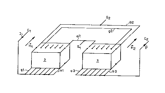
The sche~stlc arr~ngement shown ln Flg. 3 la slmllnr to the
~rr~ngement shown in Fig. 2a, but has the advnnt~ge th~t now only
nrrnngements 2 ~nd 3 are left. Because of thi~ the connsction to
the two current termin~ls C1 and C2 ~re located on the lower
surface of the arrangementc 2 ~nd 3 ~nd not, MS in Fig. 2n, on
the upper sides of the srr~ngements 1 And 4.
Th~ cche~atic ~rr~nge~ent ~hown in Fig. ~ is id~ntic~l to the
arr~ngement chown in Fig. 3~ with the exception th~t the
connection on the surface of arrangements 2 ~nd 3 run no longer
p~rallel to each other, but cross ench other. Becauee of this
the reluti~e position of the three ~bo~e-mentioned vectoricl
directions no longer m~tch the originnl position. The m~gnetic
field hns pr~cticnlly shi~ted its relutive position ~t the
locatlon of arrangement 3 by 180. This means thut the Hall
element shown in Fig. 4 no longer me~sure~ the sum H1 ~ H2, ne
the Hull element ~hown in Fig. 3, but the difference H1 - H2 of
two magnetic fields H1 ~nd H2, whereby hl i~ the mngnetic field
at the locntion of ~rrsnge~ent 3, cnd h2 i~ the m~gnetic field at
the loc~tion o Arrnngement 3. In other word~: the H~ll element
shown in Fig. 4 cnn ~e used to mensure ~ m~gnetic fi~ld gr~dient
between two points ~epnrated in ~pnce.
The Hall e~ement shown ~chemntic~lly in Fig. S is nearly
identical to thnt shown in Fig. 3, with the difference th~t the
- '
lZ6376~
two ~rr~ngement~ 2 ~nd 3 are not ne~rly ~ligned ln ~ row next to
e~ch other, but ~re ne~rly oligned in a row behind esch other.
However, the connection~ which ~re uppermo~t in the embodiment of
the dr~wing run crosfiwise, thi~ time in order to le~ve the
rel~ti~e po~ition of the three Yectori~l direction~ unchanged.
Fig. 6 ~how~ the practic~l resliz~tion of the H~ll element ~hown
in ~chem~tic repre~entation in Fig. 3, whereby ~ vertic~l H~ll
element i~ ag~in produced. The H~ll element ~hown i~ ne~rly
identic~l to the integrated vertic~l ~411 element ~hown in Fig.
2b, with the difference that thi~ time only two ~rrangements 2
~nd 3 are pre~ent.
The poLnta to be connected to ~ current termln~l C1 or C2,
loc~ted on the lower ~ides of the two arr~ngemen~ 2 ~nd 3 which
cre now outermoet now ecch constitute one singln common buried
layer ~1; bl; cl; dl or ~3; b3; c3; d3 per ~rrangement 2 or 3,
eDch connected with one current terminal C1 or C2 of the H~ll
element ~$a a deep diffu~ion 20 or 21 extending fully through the
semiconductor layer 5 to the surf~ce of the H~ll ele~ent, i.e. of
the intesrated circuit. The deep diffu~ions 20 ~nd 21 ~re made
of a material of the same materi~l conductivity type a8 the
buried layer6 ~nd is heavily doped with foreign atom~ 08 said
buried layers, l.e. It con~ists of N~ ~ateri~l.
~ 2~i3764
- 12-
The integrated vertical Hall elements realized
according to Figs. 2b and 5 have the advantage that,
in contrast to known vertical Hall elements the two
current terminals Cl and C2 of which are built very
differently and have very different dimensions,
possess exactly symmetric properties in both current
directions.
To ensure long-time stability, the surface of the
semiconductor layer 5 in Fig. 6 is coated with a thin
surface layer 22 which is made of the same material P
as the substrate 6. All contact diffusions 7 to 12,
all connectors 16 to 18 and the two deep diffusions
20 and 21 fully traverse this thin surface layer 22.
The vertical Hall element shown in Fig. 2b is also
provided to advantages with such a thin surface layer
22, but this is not shown in Fig. 2b.
The two figures 7 and 8 show respectively the cross
section VII and the top view of one and the same
horizontal Hall element. It too consists of two
arrangements 2 and 3, but these are not aligned in a
row next to each other but, as seen from above, are
turned against each other by an angle of nearly 90
degrees and located in the semiconductor layer 5.
The spatial arrangement and the material of substrate
6, of the semiconductor layer 5, of the surface layer
22, of the insulation layer 19, of the metallization
and of the connectors 16, 17 and 18 of the insulation
rings which are designated 23 and 24 in Fig. 8, are
the same as in Fig. 6. All connections al to dl, a2
to d2 and a3
~Z6376~
to d3 ~re loc~ted ln form o metslllz~tlon~ ~t the ~urfece o the
integr~ted circult. Thue, there 4re no buried layers in thi~
c~se. Theee h~ve been repl4ced by cont4ct diffu~ion~ 25 to 32,
whereby the contsct diffu~ionc 25 to 28 on the one h~nd, ~nd the
cont~ct diffusions 29 to 32 on the other h~nd ~r~ lined up to
~dv4nt~ge ~e~rly in ~ str~ight row. The cont~ct diffueion~ 25
to 32 ~re ~11 made of the ~me N~ m~terial ~ the cont~ct
diffueion~ 7 to 12. The connection lines of the center~ of the
two cont4ct dlffuslon rowL 25; 26 27 28 4nd 29; 30; 31; 32 form
ne~rly ~n ~ngle of 90 to ~ch other. E~ch of the ~rr~ngement~ 2
4nd 3 i8 provided with two cont4ct diffusions row~ 25; 26; 27: 28
~nd 7: 8: 9 or 10; 11; 12 ~nd 29; 30; 31; 32, whereby e~ch
cont~ct diffueion of one row f~ces the other row ~t the surf~ce
of the ~emiconductor 14yer S. In e~ch of the two cont~ct
diffusion row~ 7; 8; 9 4nd 10; 11; 12 4 cont~c~ diffusion without
number is dr~wn in Fig. 8, f~cing tho cont4ct diffusion 26 or 3~.
E~ch of the cont~ct diffu~ion6 7 to 9 on the one h~nd, ~nd 10 to
12 on the other h~nd, 4re ~180 ~rr4nged to ~d~hntage in ~
~tr~ight row th~t ic preferubly p4r~11el to the cont4ct diffusion
row 25: 26; 27; 28 or 29; 30; 31; 32. The connection~ 42 to d2
connect the contuct diffu~ion~ 7to 9 electric~lly to the cont~ct
diffu~ionF 10 to 12, whereby the e~ch of the connection~ u2 4nd
d2 ie provided with 4 sen~or connection S1 or S2 recpecti~ely.
The first termin41 Cl of the H411 element is connected ~i~
connections ~1 to dl to the cont~ct diffu~ion~ Z5 to 28, 411 four
of which belong to ~rr4ngement 2. The second ter~in~l C2 of the
13
1.26376~
Hall element is connected vl~ connectlons ~3 to d3 to the cont~ct
diffusLons 29 to 32, ~ll four of which belong to ~rr~ngement 3.
The horizont~l Hall element shown in Fige. 7 to 8 h~e the
~d~nt~ge th~t it~ null volt~ge (offset volt~ge) is compen~ted
extensively, ~ will be expl~ined in further dat~il below through
Figs. 94 4nd ~b.
Fig. 9~ shows ~ diplexer m~de up of four resist~nces ~nd
represents the equi~lent circuit di~gr~m of ~ convention~l H~ll
element. The diplexer ~ont~ins two different resist~nce v41ues
R~nd R~ _ R, whereby e~ery two resist~nces which are p~rallel in
sp~ce, i. e. two reslstances f~cing e~ch other ln dismetrlc~l
opposition in the diplexer, are equsl. The resist~nce difference
_ R ie cre4ted by piezoresistive effects, geometric tolar~nces,
etc. In ~ m~gnetic field H = O ~ null ~oltage Vof~ =
( ~ R~R)VCl,C2 occur~ ~t the eensor exit Sl; S2 of the H~ll
element whereby V
Cl,C2 repre~ente a ~upply current existing ~t
the current term~n~ls Cl, C2 of the H~ll element.
The equi~alent circuit di~gr~m of the horizont~l H~ll ~lement
chown in Figs. 7 to 8 is reproduced in Fig. 9b. It
differenti~tee itself from the equi~41ent circuit di~gr~m chown
ln Fig. 9~ in th t one h~lf of the diplexer i8 turned ~w~y by
90 angle rom the other h~lf. Slnce two resl~t~nce~, parallel
in sp~ce, ~re ~guin equ~l to R or R~ _ R, two equ~l resist~nce
14
1263764
are allgned in ~ row ln this ca~e, ~8 aeen in the dlrectlon of
flow of the supply current I, which le~de to V ff b i O
ullific~tion of the null volt~ge V
off c~n be ~chleved in ~
vertic~l H~ll element (~ee Fiy. 3) by repl~cing the short circuit
connections a2 ~nd bZ with two row~ of switched resist~nce~ <not
shown) with their Joint pole being connscted to one of the sensor
connections S1 or S2. These resist~nces should be ~d~ust~ble
b~l~ncing resietance~. Such ~ reei~tance fihould prefer~bly
consist, for example, of ~ resistive 14yer field effect
tr~nsistor (RLFET) or of ~ MOS field effect tr~nsistor the
source-drain ch~nnel resist~nce of which represents th~t
rssistsnce the resistance value of which csn be ~dJusted by
me~ns of the g~te volt~ge of the field effect tr~nsir-tor.
All of the integr~ted H~ll elements described c~n be m~de
~ccording to st~ndsrd bipol~r integr~ted circuit technology.
Th~nks to the utiliz~tion of H~ll elements which are subdivided
~ever~l times, H~ll elements of ~ny desired size c~n b~ reslized
even though ~ thin epit~xy layer in form of semiconductor l~yer 5
is pre~ent. This h~G the ~dv~nt~ge th~t the non-line~rities of
the H~ll element ~re kept down ~nd it~ l/f noise i~ low.