Note: Descriptions are shown in the official language in which they were submitted.
4~ ~
FREQUENCY SYNTHESIi~ER
BACKGROUND OF THE INVl;:NTION
The present invention relates to a ~requency synthesizer
applicable to radio communication equipment.
A prior art ~requency synthesizer of the kind described
5 includes a variable frequency divider for div;ding as~ output
frequency of a voltage controlled oscillator to a predetermined
frequency, a fixed frequsncy divider For dividing an output
~requency o~ a reference oscillator, and a phase comparator for
comparing the phases of outputs of the two frequency diviclers to
10 produce a volta~e which is representative of a dif~erence between
the two phases. The output of the phase comparator is applied
to the voltage controlled oscillator to control the oscillation
fre~uency thereof, thereby Producing a desired frequency. A
power source Yolta~e is constantly applied to the voltage
15 controlled oscillator and intermittently applied to the two
frequency dividers, the phase comparator and the reference
oscillator. A problem is that the prior art synthesizer needs a
long lock-up time because of the intermittcnt power source
Yoltage snpply. Another problem is that substantial power is
2 û consumed even in a battery saving condition because a power
source ~oltage is constantly applied to the voltage controlled
oscillator .
SUMMARY OF THE INYENI`ION
~5 It is therefore an object o~ the present invention to provide a
frequency syrlthesizer which with a simple constructio~ succeeds
in shortening the lock-up time.
It is another object of the Present in~ention to Provide a
~ ~,
-
~2~4~;~7
-2
~requency synthesizer which cuts dowll power consumPtion in a
battery saving condition.
It is still another object of the present inYÆntion to pro~ide a
~enerally improved frequency synthesizer.
A frequency synthesizer which controle; an oseillation
frequency of a voltage controlled oscillator and is ener~ized by a
power source of the present invention comprises a first
frequency divider for dividing an output frequency of the voltage
controlled oscillat~r, a second frequency divider for dividing an
output ~requency of a refercnce oscillator, a phase comparator
for comparing a phase of an output of the first frequency
divider and an output of the second frequency divider, a voltage
outputted hy the phase comparator b~ing fed back to the
voltage controlled oscillator via a low-pass filter, a first switc:h
connected between the phase comparator and the low pass filtor,
and a reset circuit interloctced with the power source for
producin8 a reset signal, the reset signal ~rom the reset circuit
resetting the first and second frequencY dividers, the fi~st switch
being closed after the reset signal has been produced and opened
at an instant when the power source has been turned off.
The synthesizer maY further comprise a eecond switch which
is opened and closed bY a ~attery saving control signal applied
to the second switch, thereby supplying an intermittent power
voltage to at least the first and second frequency dividers.
2 5 The synthesizer maY further comprise a delay circuit
connected to an output terminal of the second switch for
controlling opening and closing of the first switch responsiYe to
an output of the second switch.
The above and other obiects, features and advantages of the
present invention will become more apparent from the following
detailed description taken with the accompanying drawings.
BRIEF DESCRIPTION OF THE DRAWINGS
Fig. 1 is a block diagram showing a prior art frequency
synthesizer; and
~9 ~ A ~D~Y"il
--3--
Fi~. 2 is a block dia~rarn of a frequency synthesizer
embodying the present inYention.
DESCRIPTION OF THE PREFERRED EMBODIMENT
While the frequency synthesizer of the pr~esent invention is
susceptible of numerous phYsical embodiments, depending upon
the environment and requirements of use, a substantial number
of the herein shown and described embodiment have been made.
tested and used, and all have performed in an eminently
s~tisfactory manner.
To better ui~derstand the present invention, a ~rief reference
will be made to a prior art frequency synthesizer, sho~ivn in Fi~.
1. As shown, the frequency synthesizer, generall~ 10,
comprises an input terminal 12 to wbich a batter~r sa~ving control
signal is applied, an output terminal 14, and a source input
terminal 16 adapted so power the whole synthesizer. Source
volta~es Vcc and Vb are fed to the various structural elements of
the synthesizer 10.
In detail, the synthesizer 10 comPriseS a low pass filter
(LPF~ 18, a ~oltage controlled oscillator (VCO) 20 the output
frequency of which is controlled by an output of the LPF 18, a
variable frequencY divider 2 2 functioning to dil~ide an output
frequency of the VCO 2 0 to a predetermined frequency,
reference oscillator 24, a ~ixed ~requency divider 26 adapted to
divide the output ~requency of the reference oscillator 24, and a
phase comparator 28 adapted to compare the phases of the
outputs of the frequenc~ di~riders 22 and 26 and produce a
voltage representati~e of a difference there~etween. The
synthesizer 10 further comprises a SGurCe switch 30 which is
opened and closed by the battery savin~ consrol signal applied to
the terminal 12, a delay circuit 32 connected to an output
termi~al of the source switch 30, and a switch 34 supplied with
outputs of the phase comparator 28 and delay circuit 32 and
opened and closed by the output o~ the deia:7 circuit 32. When
35 the switch 34 is closed, the ousput voltage of th~ phase
~2~;~82~7
comparator 28 is deli~ered via the LPF 18 to the YCO 20 so as to
control the VCO oscillation frequency. While the switch 30 is
closed, the voltage Vcc is fed to the various elements of the
synthesizer 10 as illustrated.
Under some conditions, the voltage Vcc may be applied to
only the frequency dividers 22 and 26.
In operation, the frequency osc~llated by the re~erence
oscillator 24 which is accurate and stable and the output
~requency of the Vt:O 20 are individually divided and then appiied
to the phase comparator 28. Comparing the phases of the two
input frequencies, the phase comparator 28 produces a voltage
representative of a phase difference therebetween. Thus volta~,e
is ~ed to l;he VCO 20 to control its oscillation frequency, whereby
a ~esired frequency is attained with the accuracy of tho oscillator
24.
The prior art frequency synthesizer 10 constructed and
operated as described above has some drawbacks, as pointed
out by the preamble of the instant specification. Namely, the
lock-up time is lon8. In addition, because the volta~e V~ is
constantly applied to the VCO 2Q, power consumPtiOn in a
battery saving condition is substantial.
In light of this, in accordance with the present invention,
when a source switch is closed to apply a voltage, a reset signal
is fed from a reset circuit to a variable frequency diYider and a
2 5 fixed frequency divider. hfter the reset signal has been
outputted, the switch is closed so that an output voltage of a
phase comparator is applied to a VCO to control the oscillation
frequeney of the ~CO. At the instant when the power switch is
turned on and then off after the synthesizer has been once
locked, the frequency o~ the VCO is substantially the same as the
locked ~requency. Hence, as the variable and the fixed
frequency dividers are reset, the output of the phase comparator
is approximated to a steady outPut with the result that the
lock-up times is shortened.
3 5 A preîerred embodiment of the present inve~tion will be
3L2~
described in deail hereinafter.
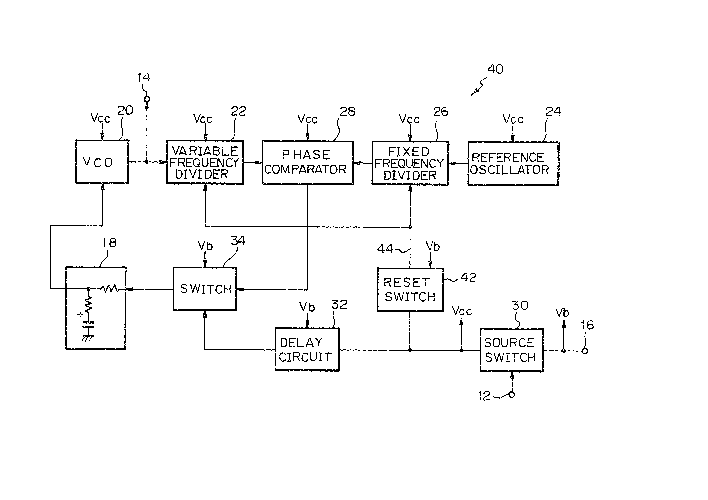
Re~erring to Fig. 2, a frequency synthesizer embodyin~ the
present inv~ntion is shown and generally designated by the
reference numeral 4û. In Fig. 2, the same structural elements
as those of Fig. 1 are designated by like reference numerals. As
shoYYn, the synthesizer 40 includes, in addition to the~arious
elements oî the prior art synthesizer 10, a reset circuit 42
adapted to produce a reset signal interlock~d with a power
source of the synthesizer 40. The reset signal 44 is applied to a
Yariable frequency divider 22 and a fixed frequency divider 26 to
reset them.
In operation, the output frequencY of a VCO 20 is divided by
the variable frequency divider 2 2 to a predetermined frequency
and, then, applied to a phase comparator 28. Meanwhile, tbo
output ~requency of a reference oscillator 24 is divided by the
fixed frequencY divider 2 6 and, then, applied to the phase
comparator 28. The phase comparator 28 compares the phases
of the frequency dividers ~2 and 26 to produce a voltage which
is r epresentative of the resultant phase difference. A source
2 0 voltage is applied to a source input terminal 16 to power the
entire syrlthesizer 40. A battery saving control sig~al is fed to
an input termi~al 12 to turn on and off a source switch 30.
While the switch 30 is turned on, a voltage Vcc is applied to the
various elements of the synthesizer 40.
2 5 Under some conditions, the voltage vcc may be applied to
only the ~requency dividers 22 and 26.
When the switch 30 has bee~ turned on and the ~olta8e Vcc
has been applied, the reset circuit 42 produces a reset signal for
res0tting the Yariable and the fixed frequency dividers 22 and
26. A delay circuit 32 deli~ers an ON signal to a switch 34 after
the voltage Vcc has been applied via the switch 30 and the reset
sig~al 44 has been deliYered from the reset circuit 42. Whell the
switch 30 has been turned off, an OFF signal is applied to the
switch 34 at the same time.
While the switch 34 is turned on, the output voltage of the
31L2~
phase comparator 28 is routed through a LPF 18 to the ~CO 20.
While the switch 34 is turned off, an output voltage of the phase
comparator 2~ which has appeared immediatelY before the
turn-off of the switch 34 is held by a capacitor lBa of the LPF
5 18. ~enerally, the Period of time during which the capacitor
18a holds th~ ~utput voltage of the phase comparator 28 is
determined by thE~ capacitance of the capacitor 1 ~a, the input
impedance of the VCO 2 0, and the OUtp'lt impedance of the
switch 34. In accordance with the present invention, the switch
10 34 is constructed to turn off after a period of time which is far
shorter than the holding time of the capacitor 1 8a. While the
switch 34 is turned off. the output of the phase comparator 28
is fed back to the Vt::O 2 0 via the LPF 18 so that the VCO
oscillation frequency is controlled by a DC voltage which is
15 outputted by the LPF 18.
At the iDstant when She switch 30 is turned off and then on
after the synthesizer 40 has been once locked, the output
frequency of the VCO 20 is substantially equal to the frequency
which has been locked by the ~oltage held by the capacitor 18a.
20 As a restllt, when She frequency dividers 22 and 28 are reset,
the output of the phase comparator 28 îS approximated to the
steady output which has appeared during the locked condition,
thereby shortening the lock-up time.
In summary, it will be seen that the present invention
25 provides a frequency synthesizer which shortens lock-up time
and cuts down power consumption in a battery saving condition
without resorting to complicated means. Specifically, the only
element needed besides those of the prior art is a reset circuit
which produces a reset signal interlocked with a power source of
30 the synthesizer so as to reset a variable and a fixed fre~uency
dividers, thereby reducing a phase difference bet~qeen the
outputs of the frequency dividers within a short Period of time.
Various modifications will become possible for those skilled
in the art after receiving the teachings of the present disclosure
35 without departin~ from the scope thereof.