Note: Descriptions are shown in the official language in which they were submitted.
~L2~ 37~
25711-472
BACKGROU~D OF THE INYEMTIO~
FIELD OF THE I~VE~TION
The present invention relates to a ceramic semi-
conductor device exhibitlng a positive temperature coefficient of
resistance (hereinafter referred to as positive ceramic se~i-
conductor device) which can be used as heat generating elements o~
various types or as current control elements in electric circuits.
D~SCRIPTION OF THE RELATED ART
The hitherto known positive ceramic semiconductor device
is typically of such a structure which has a pair of electrodes
each of a two-layer structure composed of a nickel layer and a
sllver layer implemented by forming first the nickel layer on each
of upper and lower sur~aces of a posltive ceramic semiconductor
substrate, and then forminy thq silver layer over the surface o~
the niakel layer.
In the hitherto known posltive ceramic semiconductor
devlce of the structure mentioned above, there takes place so-
called silver-migratlon phenomenon in which silver constituents in
the silver layer migrate along the surface of the substrate from
the electrode serving as positive pole toward ~he electrode
serving as negative pole when a predetermined potential difference
- 1 - ~
~2Ei4L93~9L
1 is applied across the paired electrodes of positive
and negative poles, respectively. The migration of
silver is significantly accelerated in the atmosphere of
high temperature and high humidity or moisture. This
phenomenon is often accompanied with formation of short-
circuit between the electrodes, degracling thus performance
of the positive ceramic semiconductor device.
Further, it is observed in the positive ceramic
semiconductor device that when a current flows through
the semiconductor substrate, the current flow is locally
concentrated, giving rise to a localized heat generation.
As the result,~crack is produced in the ceramic semi-
conductor substrate due to thermal stress, possibly
incurring unwanted degradation in the mechanical strength
of the substrate.
Under the circumstances, there exists a demand
for improving the positive ceramic semiconductor device
so as to exhibit stable characteristics by suppressing
as perfectly as possible the silver-migration phenomenon
and at the same time preventing the thexmal destruction
of the semiconductor substrate due to the localized
heat generation.
The present invention has been made with a
view to satisfying the demand mentioned above.
SUMMARY OF THE INVENTION
A first object of the present invention is
to provide a positive ceramic semiconductor device in
-- 2
64~L
3 25711-472
which occurrence of the silver-migration phenomenon on the
positive ceramic semiconductor substrate described above is
suppressed in a satisfactory manner.
With a view to achieving the above-mentioned object,
there is provided according to an aspect of the present invention
a positive ceramic semiconductor device, comprising a pair of
electrodes formed on a positive ceramic semiconductor substrate
which is constituted by a material of a barium titanate series
which exhibits a positive temperature coefficient of resistance
and has a Curie point at which resistance of the material
increases steeply at a predetermined temperature, wherein one of
said paired electrodes which is to serve as the positive pole is
formed of an electrically conductive alloy material containiny
silver and palladlum in such a ra-tlo that the content of silver
ranyes from ~0 wt.% to ~0 wt.% while that of palladium ranCJes from
60 wt.% to 10 wt.% in silver-palladium series. In consideration
of occurrence of the silver-migration phenomenon more or less,
current concentration due to interfacial resistance making
appearance on the positive ceramic semiconductor substrate and the
cost of palladium, it is preferred that the content of palladium
in the silver-palladium series should be in a range of 10 wt.% to
60 wt.%. Further, in view of the reliability of performance and
aost of the positive ceramic semiconduator devlce, the content of
palladium should more preferably be selected to be in a range of
20 wt.% to 30 wt.~.
A second object of the present invention is to provide a
positive ceramic semiconductor device which has the basic
struature proposed above and in which localized heat generation
~.26~71
4 25711-~72
due ~o the current concentration in the electrically conducting
state is prevented to ~hereby protect the ceramic semiconductor
substrate against degradation in the mechanical strength.
For accomplishing the second object mentioned above,
there is provided according to another aspect of the invention a
positive ceramic semiconductor device which has a pair of
electrodes formed on a positive ceramic semiconductor substrate
and in which one of the paired electroaes serving as the positive
pole is formed of at least an electrically conductive layer
constituted by sil~er particles having respective surfaces
deposited with solid solution layers of silver-palladium, wherein
the content of silver ranges from 80 wt.% to 98 wt.~ with that of
palladium ranging from 20 wt.% to 2 wt.% in the silver-palladium
serles.
In view of the second mentloned ob~ect, there is ~urther
provided according to still another aspect of the lnvention a
positive ceramic semiconductor device, comprising a pair of
electrodes formed on a positive ceramic semiconductor substrate
which is constituted by a material of a barium titanate series
which exhibits a positive temperature coefficient of resistance
and has a Curie point at which resistance of the material
increases steeply at a predetermined temperature, wherein one of
said paired electrodes which is to serve as the positive pole is
constituted by an electrically conductive metal layer ohmically-
contacted to said substrate and an electrically conductive layer
formed on said electrically conductive metal layer and containing
an alloy of silver and palladium, said electrically eonductive
metal layer ohmically-contacted to said substrate containing a
~26~
25711-472
metal material having a high electric conductivity as compared
with that of said electrically conductive layer containing the
silver-palladium alloy, wherein a composi1.ion of the two
constituent series of silver and palladium is so selected that the
content of silver ranges from 40 wt.% to 90 wt.% while that of
palladium ranges from 60 wt.% to 10 wt.% in silver-palladium
series.
Additionally, for accomplishing the second mentioned
object, there is provided according to a further aspect of the
invention a positive ceramic semiconductor device, comprising a
pair of electrodes formed on a positive ceramic semiconductor
substrate which is constituted by a material of a barium titanate
series which exhlbits a posltive temperature coefflcient of
resistance and has a Curie point at which resistance o~ the
material increases steeply at a predetermined temperature wherein
one of said paired electrodes to serve as the positive pole is
constituted by a single layer of an electrically conductive
material containing an alloy of silver and palladium, the
composition of the two-component series of silvei and palladium
being so selected that the content of silver ranges from 40 wt.%
to 90 wt.% while that of palladium ranges from 60 wt.% to 10 wt.%,
the other electrode of said paired electrodes which is to serve as
the negative pole being constituted by an electrically conductive
metal layer ohmically-contacted to said substrate and an
electrically conductive layer formed on said metal layer and
containing an alloy of silver and palladium, said ohmically-
contacted electrically conductive metal layer containing a metal
material having a high electric conductivity when compared with
" ~L~69~
6 25711-472
that o~ said electrically conductive layer containing the alloy o~
silver and palladium, a composition of the two-component series of
silver and palladium being so selected that the content of silver
ranges from ~0 wt.% to 90 wt.% while that of palladium is in a
range of 60 wt.% to 10 wt.%.
Furthermore, for achieving the second mentioned object,
~here is provided according to a still further aspect of the
invention a positive ceramic semiconductor device, comprising a
pair of electrodes formed on a posltive ceramic semiconcluctor
substrate which is constituted by a material of a barium titanate
series which exhibits a positive temperature coefficient of
resistance and has a Curie point at which resistance of the
material increases steeply at a predetermined temperature, wherein
one of sald paired electrodes whlch ls to serve as the posltlve
pole ls formed of at least an electrically conductlve material
co~talnlny at least silver and palladium at such a ratio that the
content of silver in the silver-palladium series ranges from 40
wt.% to 90 wt.~ while that of palladium is in a range of 60 wt.%
to 10 wt.%, the other of said paired electrodes which is to serve
as the negative pole being realized in a two-layer structure
constituted by a first electrically conductive layer formed on the
surface of said substrate ln ohmic contact therewlth and a second
electrically conductlve layer Eormed on said first conductive
layer and the surface of the ceramic semiconductor substrate so as
to cover an outer peripheral edge of said first electrically
conductive layer, said second electrically conductive layer bein~
formed of an electrically conductive material which contains at
least 40 wt.% to 90 wt.% of silver, 60 wt.% to 10 wt.~ of
.2~
7 25711-472
palladium and at least one base metal selected from a group
consisting of tin, indium, gallium, alloys of indium and gallium,
nickel, antimony and aluminum.
7a 25711-472
The ceramic substrate is preferably formed of a
barium titanate series material.
BRIEF DESCRIPTION OF THE DRAWINGS
Fig. l, Fig. 2, Fig. 3, Fig. 4 and Fig. S are
vertical sectional views showing, respectively, Plectrode
structures of positive ceramic semiconductor devices
according to basic embodiments of the present invention;
Fig. 6 is a view showing graphically chaxacter-
istics of the positive ceramic ~emiconductor devices
according to the basic embodiments of the invention for
illustrating operative features and effects thereof;
Fig. 7 is a view showing schematically a struc-
tuxe of an electrode of a positive ceramic semiconductor
device according to a modified embodiment of the prese~t
invention;
Fig. 8 and Fig. ~ are views showing character-
istics of the modified embodiment of the invention for
illustrating operative features and effects thereof;
Fig. lO, Fig. 11, ~ig. 12, Fig. 13 and Fig. 14
are vertical sectional views showing, respectively,
electrode structures of positive ceramic semiconductor
devices according to other modified embodiments of the
present invention;
Fig. 15 and Fig. 16 are views showing charac-
teristics of the positive ceramic semiconductor devices
according to the other modified embodiments of the
invention;
Fig. 17 is a view for illustrating problems of
1 the positive ceramic semiconductor device;
Fig. 18~ Fig. 19 and Fig. 20 are vertical
sectional views showing, respectively, electrode struc-
tures of positive ceramic semiconductor devices according
to further modified embodiments of the present invention;
and
Fig. 21 is a view showing charaGteristics of
the positive ceramic semiconductor devices according to the
further modified embodiments of the nvention for illustrat-
ing action and effects t~ereof.
DESCRIPTION OF THE PREFERRED EMBODIMENTS
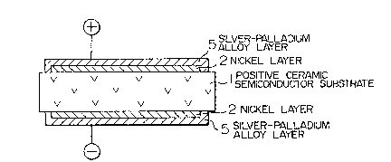
Figs. 1 to 5 show)in vertical sections~positiveceramic semiconductor devices implemented according to
basic embodiments of the presen-t invention. Re~errin~ to
Flg. 1, the positive ceramic semiconductor device includes
nickel layers 2 which are formed, respectively, on both
surfaces of a positive ceramic semiconductor substrate 1
in ohmic contact therewith, and electrically conductive
layers 5 constituted by silYer-palladium alloy layers,
respectively~ and formed on the nickel layers 2 in such
a manner as to cover the outer peripheral edge as well as
the surfaces thereof. The substrate 1 is constituted by
a material of barium titanate series which exhibits a
positive temperature coefficient of resistance and has a
Curie point at which resistance of the material increases
steeply at a predetermined temperature.
In the case of the abovementioned positive
~ 64~71
1 ceramic se~iconductor device shown in Fig. 1, the
electrode destined to serve as the electrode of~lpositive
pole is realized in a two-layer structure of the nickel
layer 2 and the silver-palladium alloy layer 5. In
contrast thereto, a positive ceramic semiconductor
device shown in Fig. 2 has the positive pole electrode
which is constituted only by a single silver-palladium
alloy layer 5. It will however be noted that the
negative pole electrode is of the same structure as the
one shown in Fig. 1.
In the case of a positive ceramic semiconductor
device shown in Fig. 3, the positlve pole electrode is
of the same structure as the one shown in Fig. 1. On
the other hand, the negative pole e~ectrode is realized
in a two-layer structure constituted by a nickel layer
2 and a silver layer 3 similarly to that of the hither-
to known positive ceramic semiconductor device.
In a positive ceramic semiconductor device
shown in Fig. 4, the positive pole electrode is of the
same structure as the one shown in Fig. 2 while the
negative pole electrode is realized similarly to that of
the hitherto known device as in the case of the embodi-
ment shown ln Fig. 3.
The positive ceramic semiconductor device shown
in Fig. 5 differs from those shown in Figs. 1 to 4 in
that the positive ceramic semiconductor substrate is
realized in a ring-like configuration rather than the
disk-like configuration adopted in the devices shown in
g
1 Figs. 1 to 4. The electrode structure of the embodiment
shown in Fig. 5 is identical with that of the device
shown in Fig. 1.
Next, a method of fabricating the positive
ceramic semiconductor device according to the invention
will be described in conjunction with the embodiment
shown in Fig. 5, by way of example.
Both surfaces of a ring-like positive ceramic
semiconductor substrate (fired product) 1 of a material
belonging to barium titanate series and manufactured by
a conventional method are ground by an abrasive particulate
material, e.g. abrasive particles of silicon carbide.
After cleansing, the ground substrate is dried.
Subsequently, an activated paste containing
~5 palladium chloride which may be the one available under
the trade name "K146" from Japan Kanizen Co. Ltd. is
screen-printed over both surfaces of the substrate.
After drying, the paste is fired or baked at a temperature
of 400C to 700C.
After the baking process, the substrate is
immersed in a nonelectrolyte plating bath of I~i-P series
to be plated with nickel. Thereafter, firing is performed
at a temperature of 200C to 450C, to thereby form nickel
layers on both surfaces of the substrate, respectively.
Subsequently, a paste containing silver particles
of size less than 1 ~m on an average and palladium
particles of 800 A in size on an average is applied over
each of the nickel layers thrcugh screen printing, the
-- 10 --
~2~7~
1 resultant product being then baked at a temperature of
600C for 15 minutes, whereby silver and palladium are
all transformed to a solid solution constituting a two-
element alloy.
It will be understood that the positive ceramic
semiconductor devices shown in Figs. 1 to 4 can also be
manu~actured according to the process described above.
A plurality of specimens of the positive ceramic
semiconductor devices manufactured according to the process
mentioned above and in which the proportion or ratio of
contents of silver and palladium was changed were pre-
pared and examined in respect to the migration proof
property and the interfacial resistance. The results of
the examination will be described below.
Each of the positive ceramic semiconductor
substrates employed in the specimen was implemented in a
ring-like configuration shown in Fig. 5 and has an
outer diameter o~ 35.0 mm, an inner dia~eter of 25.0 mm
and a thickness of 2.5 mm. These specimens were subjected
to a continuous conduction withstanding test at a room
temperature by applying a voltage of 14 V continuously
for 2000 hours in an air stream at a flow rate of 20 g/sec.
The results of the test are illustrated in
Fig. 6 in which distance covered by migration is taken
along the left-hand ordinate, while the interfacial
resistance (~R) is taken along the right-hand ordinate.
The interfacial resistance is determined in accordance
with the following expression:
;4~37~
~R = (~ i - Ag/Pd RN~
1 where ~ i represents the resistance value of the positive
ceramic semiconductor device (of the configuration and
dimensions mentioned above) which has, however, both
electrodes of positive and negative pole which are made
of nicle (formed by baking at 300C for two hours), and
~i Ag/Pd represents the resistance value of the posi-
tive ceramic semiconductor device having positive and
negative pole electrodes each realized in the two-layer
structure of the nickel layer and the silver-palladium
alloy layer as described hereinbefore in conjunction with
the manufacturing method. Saying in another way, the
interfacial resistance (~R) represents in terms of ratio
the difference between the resistance value of the nickel
electrode employed as the reference value and that of the
electrode according to the invention.
It will be seen from Fig. 6 that significant
change occurs in the silver-miyration phenomenon across
a boundary corresponding to the content of palladium
of 10 wt.% and that no migration phenomenon takes place
in a range in which the content of palladium is not less
than 10 wt.~.
The ma~imum coverage distance of the migration
is about 1.5 mm in the hitherto known positive ceramic
semiconductor device, which means very poor performance
of the device.
On the other hand, the interfacial resistance
- 12 -
` ~26~71
1 is increased progressively as the content of palladium
increases beyond the ratio of about 40% with the rate of
increasing in the interfacial resistance becoming signifi-
cant when the content of palladium increases beyond 60%~
It should be noted that the interfacial
resistance is definitely determined in dependence on the
electrode structure. Accordingly, the aforementioned
expression holds true for the positive ceramic semi-
conductor device shown in Fig. 1 since this device
differs from the one shown in Fig. 5 only in respect to
the geometrical configuration. However, in the case
of the positive ceramic semiconductor device shown in
Fig. 3 in particular, the reslstance value oE the
electrode as used must be substituted for ~ i Ag/Pd
in the aforementioned expression.
Thus, the characteristic curve of the inter-
~acial resistance of the positive ceramic semiconductor
device shown in Fig. 3 differs from the one illustrated
in Fig. 6. However, the content ratio of 60 wt.%
defining the upper limit of the allowable palladium
content range delimited due to the interfacial resistance
also ap~lies valid to the device shown in Fig. 3 similarly
to the one shown in Fig. 5. In the case of the embodi-
ments shown in Figs. 2 and ~, respectively, the electrode
structure is in non-ohmic contact without incorporating
the Ni-layer. Thus, it is impossible to measure the
interfacial resistance. Accordingly, the interfacial
resistance was determined on the basis of the rush current,
~2~7~
25711-472
from which it has been found that the content ratio of 60 wt.% o
palladium defines the upper limit of the allowable content range
for palladium also in these embodiments.
The positive ceramic semiconductor devices according to
the embodiments of the invention described above are excellent in
respect to their corrosion proof when used in gasoline, in view of
the fact that palladium exhibits a high withstanding capability
and durable to sulfur and chlorine. Accordingly, these positive
ceramic semicondutor devices can be used in gasoline in the expo-
sed condition without any need for protecting the electrodes.
~ s will be appreciated Erom the foregoiny description,
the positive ceramic semiconductor device according to the invent-
ion resides in a structure which includes a pair of electrodes
provided on both surfaces of the positive ceramic semiconductor
subtrate, the one of the paired electrodes to serve as the
positive pole electrode is formed of an electrically conductive
alloy material containing silver and palladium, wherein compositi-
20 on of the silver-palladium, series is so selected that the content
of silver lies within a range of 40 wt.% to 90 wt.% while that of
palladium is in a range oE 60 wt.% to 10 wt.%.
In the illustrated embodiments, the migration proof pro-
perty is enhanced as the content of palladium increases, and no
migration phenomenon takes place any
- 14 -
!379L
1 more when the content of palladium is increased beyond
10 wt.%. If the content of palladium greater than
40 wt.% is employed, the interfacial resistance makes
appearance between the positive ceramlc semiconductor
substrate and the electrode, giving r:ise to correspond-
ing reduction in the rush current, whlle the surface
resistance is increased to decrease the contact region
to a point contact, providing a cause for the current
concentration. Besides, increased content of palladium
makes the positive ceramic semiconductor device more
expensive. Thus, from the practical and economical
viewpoint, it is preferred that the content of palladium
should not go beyond 60 wt.%.
In brief, the content of palladium in the
silver-palladlum series should preerably be in a range
oE 10 wt.% to 60 wt.~ and more preferably in a range of
20 wt.% to 30 wt.% when considering the reliability in
performance and the cost involved.
As described hereinbefore, the silver-migration
phenomenon propagates from the positive pole electrode
toward the negative pole electrode. Accordingly, the
~7~
silver-migration phenomenon can be prevented by using thc
electrically conductive material of~sllver-palladium
series according to the invention in forming the positive
pole electrode even when the negative pole electrode is
of the conventional structure. The positive pole electrode
may be realized either in a two-layer structure composed
of a nickel layer formed on the surface of a positive
- 15 -
7~
l ceramic semiconductor substrate and a silver-palladium
alloy layer formed on the nickel layer or in a single-
layer structure composed of a silver-palladium alloy
layer formed on the surface of the positive ceramic
semiconductor substrate.
The negative pole electrode may be realized in
a two-layer structure composed of a nickel layer and a
silver layer formed thereon or in the same two-layer
structure as that of the positive pole electrode.
The present invention is not restricted to the
illustrative basic embodiments described above but suscep-
tible to various modifications as mentioned below.
1) Third constituent or component such as various
types of frits, bismuth or the like may be added in
addition to silver and palladium for enhancing the bondin~
strength, brazing feasibility and other properties.
2) As the method of fabricating the electrode
containing silver and palladium, there may be adopted a
sputtering method, chemical vapor deposition ~CVD),
vacuum evaporation and others in addition to the paste
printing method.
3) The nickel layer may be replaced by other metal
layer capable of forming ohmic contact with the sub-
strate l such as, for example, aluminum and bronze.
4) The geometry of the positive ceramic semi-
conductor device is neither restricted to the disk-like
configuration nor the riny-like configuration but may be
of any given shape inclusive of a honeycomb structure
- 16 -
~;~6~L871
1 having a number of through-holes in the axial direction.
5) The pair of electrodes may be formed on one
surface of the positive ceramic semiconductor substrate
with a distance between the electrodes instead of forming
the electrodes on both opposite surfaces of the sub-
strate, respectively.
Now, description ~ill be made of a modified
embodiment of the present invention. The structure of
the basic embodiments described above suffers a problem
in that when a current is supplied to the positive ceramic
semiconductor device according to the basic embodiment of
the invention, the current flow tends to concentrate at
a location to bring about a local heat generation, as a
result of which the ceramic semiconductor substrate
might be cracked to decrease the mechanical strength.
With the modi~ied embodiment, it is intended to elimi-
nate such shortcoming.
A structure characterizing the modified embodi-
ment of the invention is shown in Fig. 7. More sepcifical-
ly, this figure shows a structure of the aforementionedelectrically conductive layer constituting the electrode
according to the invention on an enlarged or microscopical
scale. According to the teaching incarnated in the
modified embodiment, an electrically conductive layer
15 is formed of silver particles ~5a each having a
surface coated with a solid solukion layer of silver and
palladiu~ 15b. This electrically conductive layer 15
is used in place of the electrically conductive layer 5.
- 17 -
,~ ID~
~ ~ ~ aL
1 ~ereinafter, this layer 15 will be referred to as the
silver-silver/palladium layer 15.
With respect to other structural features, the
positive ceramic semiconductor device according to the
modified embodiment is utterly same as those of the basic
embodiments shown in Figs. 1 to 5. Besides, the method
of manufacturing the positive ceramic semiconductor
device according to the modified embodiment under consider-
ation is substantially same as the method of the basic
embodiments described hereinbefore except that a prepared
paste containing silver and palladium is screen-printed on
the nickel layers formed on both sur~aces o~ the ceramic
semiconductor substrate and baked at a temperature of
600C for 15 minutes. According to a method o~ preparing
the aforementioned paste, silver powder having particle
size of 2 ~m to 3 ~m on an a~erage and palladium powder
having particle size of 800 A on an average are mixed at
a ratio o~ 90 wt.% of silver and 10 wt.~ of palladium to
form a silver-palladium powder mixture. The resultant
powder is dispersed homogeneously in an organic binder
(e.g. ethyl cellulose) to prepare the paste.
The silver-silver/palladium layer 15 obtained
after baking the paste was analyzed through X-ray
dif~raction. It has been observed that peaks of
intensity occur at silver and silver/palladium solid
solution tforming an alloy). Thus, it is determined
that the surface of each silver particle is formed with
a layer of silver/palladium solid solution.
- 18 -
8~
1 Although the past preparing method has been
described in conjunction with the positi~e ceramic
semiconductor device shown in Fig. 5, the devices shown
in ~igs. 1 to 4 can be fabricated according to the manu-
facturing method described just above.
A plurality of specimens of the positive ceramic
semiconductor devices manufactured through the process
mentioned above in which the proportion of contents of
silver and palladium was changed were prepared and examined
in respect to the migrationproof property and the surface
resistance. The results of the examination will be
described below.
Each of the specimens was implemented in a
riny-like configuration shown in Fig. 5 and had an outer
diameter of 35.0 mm, an inner cliameter of 25.0 mm and
a thickness of 2.5 mm. These specimens were subjected
to a continuous conduction withstanding test at
a room temperature by applying ~oltage of 14 V continuously
for 2000 hours in an air stream at a flow rate of 20 g/sec.
T~e substrate of each specimen had a resistance of 1.5 Q
at 20C.
The results of the test are illustrated in
Fig. 9~ in which distance covered by the migration is
taken along the left-hand ordinate, while the surface
resistance is taken along the right-hand ordinate. The
surface resistance (~) was measured by contacting probes
to the electrode surface at two discrete points.
Referring to Fig. 9, it will be seen that the
- 19 -
- ~64sn
1 migrationproof property undergoes significant change
across a boundary corresponding to the palladium content
of 2 wt.% in the silver-palladium series. When the
content of palladium increases beyond this boundary, no
migrationphenomenon takes place at all. In contrast,
the surface resistance of the electrode itself is progres-
sively increased. When the content oE palladium exceeds
20 wt.%, change in the surface resistance becomes more
significant. On the other hand, so long as the
content of palladium is within a range of 5 wt.% to
10 wt.%, no migration phenomenon takes place at all with
the surface resistant being substantially zero, indicat-
ing excellent per~ormance of the positive ceramic
semiconductor device.
As will be appreciated from the above des-
cription, the positive ceramic semiconductor device
according to the embodiment described just abo~e
includes a pair of electrode provided on a positive
ceramic semiconductor substrate, one of the paired
electrodes which is to serve as the electrode of positive
pole being constituted by at least an electrically con-
ductive layer containing silver particles having respective
sur~aces formed with silver-palladium solid-solution
layers, wherein content of silver in the silver and
palladium series is so selected as to lie within a range
of 80 wt.% to 98 wt.% while that of palladium is in a
range of 20 wt.% to 2 wt.%.
According to this embodiment, the electrode
- 20 -
~264~7 IL
1 to serve as the positive pole is composed of the electri-
cally conductive layer constituted by silver particles
having surfaces formed with solid-solution layers con-
taining silver and palladium. In this connection, it
should however be noted that the composition of silver
and palladium as a whole exerts signiflcant influence to
the characteristics of the positive cexamic semiconductor
device.
More specifically, no migration phenomenon
takes place when the content of palladium exceeds 2 wt.%.
However, when the content of palladium exceeds 15 wt.~,
the surface resistance of the electrode itself becomes
progressively increased. Beyond 20 wt.~ of palladium
content, the increasing rate of the surface resistance
becomes siynificant, involving significant tendency oE
the current concentration.
Accordingly, the content of palladium should
preferably be so selected as to be in a range of 2 wt.%
in consideration of the migrationproof property and the
surface resistance. Further, from the standpoint of
reliability in performance and cost, the content of
palladium should more preferably lie within a range of
5 wt.~ to 15 wt.~.
It should further be added that in the elect-
rically conductive layer constituting the positive poleelectrode according to the instant embodirnent, the solid
solution layer containing silver and palladium need not
be formed on the surfaces of all the silver particles.
- 21 -
~26487~
1 For example, integral solid solution particles of silver
and palladium may be presen-t in a sparsely dispersed
state.
Also in case of the positive ceramic semi-
5 conductor device according to the instant embodiment,the silver-migration phenomenon takes place in the direc-
tion toward the negative pole from the positive pole.
Accordingly, the silver-migration phenomenon can be
prevented from occurrence by realizing only the positive
pole electrode in the inventive structure described above
even when the negative pole electrode is of a conventional
structure. Further, the positive pole electrode may be
implemented in the two-layer structure composed of the
nickel layer formed on the surface of the positive ceramic
lS semiconductor substra~e and the material layer of the
composition according to the invention described above,
respectively.
The instant embodiment is susceptible to
various version as in the case of those described herein-
before and can assure advantageous effects similar tothose attained by the basic embodiment. In a version
of the instant embodiment, a modification mentioned
below may be effectuated.
6) It is possible to prepare the paste containing
silver and palladium by mixing a prepared silver paste
and a prepared palladium paste in advance.
Additionally, another advantageous effect may
be seen in that when compared with the electrode formed
- 22 -
1 totally of the silver-palladlum solid solution the surface
reslstance of the positive pole electrode can be made
significantly low due to the presence of silver because
the silver-palladium solid solution layer is formed
only on the surface of the silver particle. Consequently,
upon current flow through the aforementioned electrically
conductive layer, the current can flow through the whole
electrode due to the presence of silver, whereby suGh
undesirable phenomenon can be positively avoided that
current concentration on a localized conducting point which
would occur in the case of the electrically conductive
layer formed totally of the integral silver-palladium
solid solution and presenting great surface re~istance
takes place to produce crack in the semiconductor sub-
strate due to localized heat generation, thus enEeeblingthe mechanical strength of the substrate.
The following description is directed to further
modified embodiments of the present invention which also
tackle the problem of the mechanical strength of the sub-
strate being enfeebled in the case of the positive ceramicsemiconductor devices implemented according to the basic
embodiment.
Now, the preferred working modes of the further
modified embodiments will be described by referring to
Figs. 10 to 14 in which like components are designated by
like reference symbols.
In Fig. 10, an ohmic-contacted electrically
conductive layer is realized in a two-layer structure
~L21~
1 constituted by a nickel layer 2 formed directly on each
surface of a positive ceramic semiconductor substrate 1
in ohmic contact therewith and an intermediate layer 6
of an electrically conductive metal material formed on the
nickel layer 2, wherein the intermediate layer 6 is formed
of the metal material having a high electric conductivity
when compared with that of an electrically conductive
layer 5 containing a silver-palladium alloy (hereinafter
referred to as silver-palladium or Ag-Pd alloy layer).
Thus, the positive and negative pole electrodes of the
- device shown in Fig. 10 are realized in a three-layer
structure inclusive of the intermediate layer 6.
According to the instant embodiment under
consideration, the intermediate layer 6 may be ormed on
lS one or more materials selected from a group consisting
of silver, aluminum, tin and bronze.
When the intermediate layer 6 is to be formed
of silver, it is required that the silver-palladium alloy
layer S be so formed as to cover the whole peripheral
edge portion of the intermediate layer 6 (refer to Fig.
10). If the outer peripheral edge portion of the inter-
mediate layer 6 formed of silver is exposed, then the
problem of the silver-migration will arise again. Of
course, in practice, only partial exposure of the outer
peripheral edge of the intermediate layer 6 in the course
of manufacturing process gives rise to no problem so far
as the e~posure is within a tolerable range. On the other
hand, when the intermediate layer 6 is formed of tin or
- 24 -
., . . ' - . .
1 bronze, it is not required to cover the whole outer
peripheral edge of the intermediate layer 6 with the
silver-palladium alloy layer 5, since the silver-
migration phenomenon is difficlt to occur ~ith these
materials.
As a version of the instant embodiment under
consideration, the electrode of the paired ones which
is to serve as the negative pole may be of course realized
in a two-layer structure including a nickel layer 2
formed directly on the substrate 1 in ohmic contact
therewith and a silver layer 3 formed on the ~ickel layer
2, as is shown in Fig. 11.
As another version of the instant embodiment,
the ohmic-contacted electrically conductive layer is not
restricted to the two-layer structure but may be con-
stituted b~ a single layar 7 ohmic-contacted to the
substrate 1 and formed of a metal material having a high
resistance as compared with that of the silver-paLladium
alloy layer. In that case, the positive pole electrode
is of a two-layer structure. Although the negative pole
electrode is of a two-layer structure in the device
shown in Fig. 12, it goes without saying that this
nagative pole electrode can be realized in the structur
shown in Fig. 10 or 11. The metal material mentioned
above may be selected from a group of materials including
aluminum, tin, bronze and silver as main components
thereof, respectively. The material containing silver
as the main component may be added ~ith one or more
- 25 -
~41~n
l components selected from a group consisting of tin,
antimony, zinc, aluminum and the like.
Fig. 13 shows another version of the embodiment
shown in Fig. 10 according to which the positive pole
electrode i9 constituted only by the single layer 5 of
silver-palladium alloy. In this device shown in Fig. 13,
the negative pole electrode is realized in a three-layer
structure including a nickel layer 2 formed directly on
the substrate l in ohmic contact therewith, an inter-
mediate silver layer 6 formed on the nickel layer 2 so asto cover the outer peripheral edge of the nickel layer 2,
and the silver-paLladium alloy layer 5 formed on the inter-
mediate layer 6.
Needless to say, the intermediate layer 6 shown
in Fig. 13 may be ~ormed o~ an element selected rom a
group of aluminum, tin and bronze in place of silver.
Alternatively, a layer of a material or composition
having in combination the characteristics of the inter-
mediate layer 2 and the nickel layer 6 may be formed on
the substrate and the silver-palladium is then formed on
the abovementioned layer to thereby implement the negative
pole electrode in a two-layer structure. In this manner,
there can be realized the same electrode structure as the
one shown in Fig. 12~
According to the embodiments under consideration,
the composition of the silver-palladium alloy layer is
so selected that the content of silver lies within a
range of 40 wt.~ to 90 wt.~ while that of palladium is in
~1 ~AQ~y~l
1 a range of 60 wt.% to 10 wt.%. As the content of palladium
increases, the migrationproof property becomes increased
as is illustrated in Fig. 16. In this context, it will
be noted that when the content of palladium exceeds
10 wt A % ~ the silver-migration phenomenon takes place no
more. In contrast, in the range of the palladium
content greater than 40 wt.%, the interfacial resistance
makes appearance between the positive ceramic semi-
conductor substrate and the electrode, involving reduc-
tion in the rush current, while the contact between theelectrode and the substrate tends to assume the form of
a point contact, providing a cause for the current
concentration. Besides, cost of the de~ice increases
as a function of the content of palladium. ~nder the
circumstances, it is desirable that the content of
palladium be smaller than 60 wt.%.
Thus, the content of palladium of the silver-
palladium series employed in the devices according to the
embodiments described above should preferably be within a
range of 10 wt.% to 60 wt.% and more preferably in a
range of 20 wt.% to 30 wt.% from the standpoint of the
reliability in performance and cost of manufacture.
Ne~t, a method of manufacturing the positive
ceramic semiconductor device according to the embodiment
under consideration will be described below in detail.
Both surfaces of a ring-like positi~e ceramic
semiconductor substrate (fired product) of a material
belonging to barium-titanate series and manufactured by
- 27 -
~Çl2~
1 a conventlonal method are ground by an abrasive particu-
late material, e.g. abrasive particles of silicon
carbide. After cleansing, the ground substrate is dried.
Subsequently, an activated paste containing
palladium chloride which may be the one a~ailable under
the trade name l'~146" from Japan Kanizen Co. Ltd. is
screen-printed over both surfaces of the substrate.
After drying, the paste is baked at a temperature of
400C to 700C.
After the baking, the substrate is immersed in
a nonelectrolyte plating bath of Ni-P series to be plated
With nickel. Thereafter, firing is performed at a
temperture of 200C to 450C, to thereby form nickel
layers on both surfaces of the substrate, respectively.
Subsequently, a silver paste i~ screen-printed
on nickel layers formed on both surfaces of the sub-
strate. After drying, the interim product is baked at
750C for 15 minu-tes. Thereafter, the sub-product is
boiled in 1,1,2-trichloro-1,2,2-trifluoroethane commercial-
ly available under the trade name "DIFLON S3" for two
minutes, being followed by cleansing and then drying at a
temperature of 120C for 5 minutes.
Next, a paste containing silver particles of
size not greater than 1 ~m on an average and palladium
pa~ti~les of 800 A on an average (the content of palladium
is 20 wt.% in Ag-Pd series~ is screen-printed on the
silver layers on both surfaces of the substrate and
fired or baked at a temperature of 600C for 15 minutes.
- 28 -
- ~Z~487~
1 Through this baking or firing pxocess, sllver and palladium
are transformed to complete or integral solid solution
forming a two-component alloy.
The structure of the positive ceramic semi-
conductor device obtained through the process describedabove is shown in Fig. 14.
The mechanical strength of the semiconductor
substrate of the device of the structure shown in Fig. 14
was examined comparatively with that of a specimen for
reference. In the devices undergone the strength test,
the substrate was of a ring-like shape having an outer
diameter of 35.0 mm, an inner diameter of 25.0 ~m and a
thickness 2.5 mm and had a resistance of 1.5 ~ at a xoom
temperature (20C). On the other hand, the specimen for
reference had positive and negative pole electrodes each
of a two-layer structure including a nickel layer formed
on the substrate and a Ag-Pd alloy layer (content of Pd
is 20 wt.~ in Ag-Pd series) formed on the nickel layer so
as to cover the outer peripheral edge portion thereof.
The test was performed by applying a voltage of
24 V between the positive and negative pole eLectrodes
for one minute and measuring the tensile strength (Kg-f)
of the semiconductor substrate by means of an autograph
device.
The results of the test are illustrated in
Fig. 15 in which the data of strength derived from the
devices undergone no voltage application are shown for
comparison purpose. As will be seen from Fig. 15, the
- 29 -
21~
1 positive ceramic semiconductor device according to the
embodiment of the invention has a high tensile strength
as compared with the specimen for reference, which
strength is on the substantially same order as that of the
device undergone no voltage application. The test has thus
proved that the positive ceramic semiconductor device
according to the instant embodiment of the invention can
enjoy an excellently high mechanical strength.
A plurality of specimens of the positi~e ceramic
semiconductor devices manufactured through the process
mentioned above in which the proportion of contents of
silver and palladium was changed were examined in respect
to the migrationproof property and the interfacial
resistance. The results of the examination will be des-
lS cribed below.
The specimens were implemented in the sameconfiguration and dimensions as described above and
subjected to a continuous current conduction withstanding
test at a room temperature by applying a ~oltage of 14 V
continuously for 2000 hours in an air ventilation at a flow
rate of 20 g/sec.
The results of the test are illustrated in
Fig. 16, in which distance (mm) covered by the migration
is taken along the left-hand ordinate~ while the inter-
facial resistance is taken along the right-hand ordinate.
The interfacial resistance (Q) was determined in accordance
with the following expresslon:
- 30 -
æ6~L
~ Ag - Ag/Pd Ni)/~i
1 where RNi represents the resistance value of a positive
ceramic substrate device (of the same configuration and
geometrical dimensions) having positive and negati~e pole
electrodes formed of nickel ~baked at 300C for two hours),
and ~i Ag Ag/Pd represents the resistance value of
the positi~e ceramic substrate device having the positive
and negative pole electrodes each of the three layer
structure including the nickel layer, the sllver layer
and the silver-palladium alloy layer as described herein-
before in conjunction with the manufacturing method. In
other words, the interfacial resis-tance (~R) represents
in terms of ratio the difference between t~le resistance
of the nickel electrode serving as a reference value and
that of the electrode according to the invention.
It will be seen from Fig. 16 that significant
change occurs in the miyration phenomenon across a boundary
corresponding to the content of palladium of 10 wt.~ and
that no migration phenomenon takes place in a range in
which the content of palladium is not less than 10 wt.%.
The maximum coverage distance of miyration is
about 1.5 mm in the hitherto known positive ceramic
semiconductor device, which means very poor performance
of the device.
On the other hand, the interfacial resistance
is increased progressively as the content of palladium
increases beyond the ratio of about ~0 wt.% with the rate
`` ~ 2~
1 of increasing in the interfacial resistance becoming
significant when the content of palladium goes beyong
60 wt.%.
It should be noted that the interfacial
resistance is definitely determined in dependence on the
elec-trode structure of the positive ceramic semiconductor
device. Accordingly, the aforementioned expression holds
! true for the positive ceramic semiconductor device shown
in Fig. 14 since this device differs from the one shown in
Fig. 15 only in respect to the geometrical configuration.
However, in the case of the positive ceramic semiconductor
substrate shown in Fig. 11 in particular, the relevant
resistance value must be substituted for ~i ~g/Pd in
the aforementioned expression.
lS Thus, the characteristic curves of the inter-
~acial resistance oE the positive ceramic semiconductor
devices shown in Figs. il and 12 di~fer from the one
illustrated in Fig. 16. However, the content ratio of
60 wt.% defining the upper limit of the allowable
palladium content range delimited due to the interfacial
resistance applies valid to the device shown in Fig. 14.
In the case of the embodiment shown in Fig. 13, the
electrode structure is non-ohmic without incorporating the
Ni-layer. Thus, it is impossible to measure the inter-
~acial resistance. Accordingly, the interfacialresistance was determined on the basis of the rush
current, from which it has been found that the content
ratio of 60 wt.% of palladium defines the upper limit of
- 32 -
~6~
1 the allowable content range for palladium also in the
case of this embodiment.
The instant embodiment is susceptible to various
versions as in the case of those described hereinbefore
and can assure advantageous effects similar to those
attained by the basic embodiment. In a version of the
instant embodiment, a modification mentioned below may be
effectuated.
7) Although it has been described that the silver
layer (intermediate layer) and the silver-palladium alloy
are formed on the nickel layer through two discrete
firing or baking processes, it is possible to form those
layers through a single baking process by appropriately
selecting t~e material of the intermediate layex, the
lS baking temperature, the baking duration and other factors.
Next, a further modified embodiment of the
present invention will be described, which embodiment is
also intended to avoid the lowering in the mechanical
strength of the positive ceramic semiconductor substrate.
After intensi~e and extensive studies performed
for making clear the cause for the unwanted lowering of the
mechanical strength of the substrate mentioned above, the
following fact has been found.
In the electrode constituted by at least an
electrically conductive alloy material containing
silver and palladium, silver is usually covered with an
oxide film. In this connection, it is noted that the
oxide film, i.e. silver oxide is a p-type semiconductor.
- 33 -
~26~87~L
l In co~trast, the positive ceramic semiconductor substrate
is an n-type semiconductor. Thus, the boundary interface
where the oxide film and the substrate are contacted
with each other forms a p n hetero-junction. Consequent-
ly, the electrode formed by using the material mentionedabove presents non-ohmlc contact to the positive ceramic
semiconductor substrate.
More sepcifically, as shown in Fig. 17, when
the negative pole electrode to be provide on the positive
- lO ceramic semiconductor substrate lOl is realized in a
two-layer structure including a nickel layer formed on the
substrate lOl in ohmic contact therewith and the afore-
mentioned silver-palladium layer containing silver and
palladium which is formed on the nickel layer 102 and
the substrate 101 so as to cover the outer peripheral
edge portion of the nickel layer 102, a current io
which should inherently flow through the non-ohmic contact
portions of the silver-palladium layer 105 and the
su~strate 101 is suppressed to a current value il which
is extremly smaller than io.
Consequently, a current l in excess (i.e.
current value of io minus il) flo~s through the outer
peripheral edge of the nickel layer 102 ohmic-contacted
to the nickel layer, as the result of which a localized
heat generation occurs at the outer peripheral edge of
the nickel layer 102 due to the excessive current flow
of i ~ io-
The fact that the tendency of localized heat
_ ~4 _
~6~7~
1 generation is observed significantly in the negative poleelectrode has been confirmed by emans of an infrared
temperature analyzer ~also called thermoviewer).
Due to the local heat generation metnioned
above, temperature of the substrate 101 is locally
increased, bringing about a correspondingly increased
resistance in the locally heated region. Under the cirum-
stance, the concentration of electric current is involved
to increase further the temperature, giving rise to
generation of cracks and hence degradation in the mehca-
nical strength of the substrate.
Now, the embodiment of the invention made with
the aim for tackling the above problem will be described
in detail. Figs. 18 to 20 are sectional vie~s showing
positive ceramic semiconductor devices according to the
instant embodiment. In these figures, same or like
elements are denoted by same reference symbols.
First referring to Fig. 18, the semiconductor
device comprises a positive ceramic semiconductor sub-
strate 1 having each surface formed with a nickel layer2 in ohmic contact therewith and an electrically conduc-
tive layer 25 containing silver, palladium and a base
metal and formed on the nickel layer 2 so as to
cover the peripheral ed~e thereof. The substrate 1 is
formed of a material belonging to barium-titanate series
having a positive temperature coefficient of resistance
and a Curie point at which the resistance value increases
steeply at a predetermined temperature.
~;2~;~L~
1 In the semiconductor device shown in Fig. 19,
the positive pole electrode is realized in a single
layer structure constituted only by the aforementioned
electrically conductive layer 25, while the negative
pole electrode is reali~ed in a same structure as that
of the device shown in Fig. 18.
In the semiconductor device shown in Fig. 20,
the positive ceramic semiconductor device 1 is configured
in a ring-like structure in contrast to the disk-like
structures of the devices shown in Figs. 18 and 19.
The electrode structure is same as that of the device
shown in Fig. 18.
No~, a method of manufacturing the positive
ceramic semiconductor device according to the instant
embodiment will be described on the assumption that the
method is applied to the manufacturing of the device
shown in Fig. 20.
Both surfaces of a ring-like positive ceramic
semiconductor substrate (fired product) of a material
belonging to barium-titanate series and manufactured by
a con~entional method are ground by an abrasive particulate
material, e.g. abrasive particles of silicon carbide.
After cleansing, the ground substrate is dried.
Subsequently, an acti~ated paste containing
palladium chloride which may be the one commercially
available under the trade name "K146" from Japan Kani~en
Co. Ltd. is screen-printed over both surfaces of the
substrate. After drying, the paste is baked at a
- 36 -
L8~
temperature of 400C to 700C.
After the bakiny, the substrate is immersed in
a nonelectrolyte plating bath of Ni-P series to be
plated with nickel. Thereafter, firing is performed at
a temperature of 200C to 450C, to thereby form nickel
layers on both surfaces of the substrate, respectively.
An Ag-Pd-base metal powder mixture containing
silver (Ag) powder and palladium (Pd) powder and added
with one of pulverized tin (Sn), indium (In) and/or
gallium (Ga), nickel (Ni), antimony (Sb) and aluminum
(AQ) is prepared and added with glass frits to prepare
an Ag-Pd-base metal paste by a conventional method.
The paste thus prepared is then screen-printed
on the nickel layer of the substrate and baked at a
temperature o~ 600C ~or 15 minutes in a baking furnace
to ~orm the electrically conductive layer of the Ag-Pd-
base metal series.
The structure of the positive ceramic semi-
conductor device manufacture through the processed
described above is shown in Fig. 20
A plurality of specimens of the positive ceramic
semiconductor devices prepared according to the method
described above and in which types of base metals as
well as amounts of addition and the content ratios of
2~ silver and palladium are varied from one to another were
prepared and tested in respect to the interfacial
resistance, the migrationproof property, the strength o
the positive ceramic semiconductor substrate and the
- 37 -
gL2Ç;~
1 moistureproo~ property, the results of the test being
shown in the tables 1 to 5.
Each of the specimens is 35 mm in outer
diameter, 25 mm in inner diameter and 2.5 mm in thickness
and has a resistance of 1.5 Q at a room temperature
(2GC). With regard to the electrode structures of the
specimens, the nickel layer is 33 mm in outer diameter,
27 mm in inner diameter while the electrically conductive
layer formed on the nickel layer is 35 mm in outer dia-
meter and 25 mm in inner diameter.
Methods for evaluating the specimens are asfollows:
Concerning Interfacial Resistance
This interfacial resistance is given in terms
lS of ratio by difference between the resistance of the
electrode structure of the specimen and that of the
nickel-silver layer serving as the reference ~alue and
expressed by
~R = (RS ~ ~i - Ag~/RNi - Ag
where RS represents the resistance of the semiconductor
de~ice of the specimen and ~i Ag represents the
resistance of the conventional (prior art) semiconductor
device provided with the negative and positive pole
electrodes of the two-layer structure including the
nickel and silver layers. It should be mentioned that
in the conventional semiconductor device, the dimensions
of the electrodes and semiconductor.substrate are same
- 38 -
` ~2E;4~L
l as those of the specimens. Criterion for the evaluation
is so established that the devices having R greater than
0.2 inclusive is regarded as being good, as indicated by
a clrcle while the devices having ~R smaller than 0.2 is
regarded as being bad as indicated by a cross X.
Concerning Strength of Substrate
The specimen was tested with respect to -the
tensile strength by applying tension at an increasing
rate of 5 mm/min by using an autograph device after a
voltage of 24 V had been applied across the positive
and negative pole electrodes for one minute. The
criterion for evaluation is so established that when
the ratio of defective devices having the strength not
greater than 6 Kg-f is 0~ among ten specimens (n - 10~,
the specimen is regarded as good, as indica-ted by a
circle while the specimen haviny -the defective ratio
greater than 0~ is regarded -to be poor, as indicated
by a cross ~.
Concerning Migratian
Each device was held in an air stream of an
air flow of 20 g/sec with a voltage of 14 ~ applied across
-the positive and negative poles for 2000 hours, and the
maximum distance covered by the migration was measured.
The criterion for evaluation to -this end is so established
that the specimens in which the maximum migration distance
is less than 0.1 mm are regarded as good and indicated
by a circle while those having the maximum migration
- 39 -
1 coverage grea-ter than 0.1 mm is regarded to be poor and
indicated by the cross X.
Concerning Moistureproof Property
Change (%) in the resistance measured before and
after boiling of the speclmen in water for two hours was
measured. This change in resistance is gi~en by
~R (Rboiled Rinitial)/Rinitial ~
Criterion for evaluation is so established that the
specimen presenting ~R smaller than ~3% inclusive is
regarded to be good and indicated by a circle, while
those presenting QR greater than +3% are regarded as
being bad, as indicated by the cross X.
- 40 -
~2~4~7 a
. ~
~ o~ X X X X X X X X o o o o
.~.~
_ _ __ _
o o o o o o o o o o o o
~ ~ _ __
~ ~o ~ o\ ~ ~ ~ ~ ~ t~ ~ ~ ~ ~ ~ ~
oOO $ +o + ~o l +o $ $ ~o + +o +
_ _ _
o~ X X o o o o o o o o o o
,~ .~ _ . __ . _
,a 3 Ln ~r ~
,~ ~ ~ ~ o
E~ XI ,~ ,~ o c~ ~ ~ ~_
_ __~ __ _ _ _ _ _ _ _
~ o o X X X X ~ X o o o o
~ o ~ ,~ ~ ~o ~ ,~ ,~ ~ ~ ~ ~ _
s~ _ o o o o o ~c o o o o o _
~ o CO Ul
H ~1 ~ l O ~ ~ ~ O O O O ~ ~ ~ ~
__ ~o _ _ _ .._ _ _ _
~:: ~ 3 O O O O O O ~I lo rl O O
~ 3 ~ __ _ _
-rl ~ O ~ O In O O O O O O
~ ~ R3~ 3o~ u~ ~o c~o ~ o~ o~ ~ ~ ~ ~ ~
- .
Z '~ ~ ~ ~r ~ ~ r~ co cs~ ,~ ~1 r~ I _
123~i4~
o o a ¦
-.1 h ~ O ~ ~ O O O
H 1:4 H 1:4 H ¢l
O X X O O O X O X
O X O O O O O O O
0~ CO In ~ ~ CO el~ ~) ~)
~`I 1~ O O O O O ~1 r l
~ ~ + +, l l ~ ~ + -t
o~ O O X O O O O O O
~,) u~ ~r, _
a) o ~ o o o ~ ~ ~ ~
_ __ .
E~ o o o O o o X o X
O O O O O O O O O
r-l ~1 r-l ,-1 -1 ,-1 ~1 ~1 -1
O O O O O O ~ O ~
_ __ _ _
O O O O O O X O X
O r-l ~ O t~l
O ~ ~ , O O O O O
CO ~0 ~ ~ ~ ~ q'
_ . _
~n ~o o o o o co
O Ln O O O O O O
) a~ C5~ ~D ~r ~ ~r ~1
_ .
~r In ~ r~ oo ~ o
~_
-- 42 --
~ ~ ~ a
~ _ _ _ _
~oX X X X X ~ X X o o o o
_ . _ _ _ .
~ ~_o, o o o o o o o o o o o _
~ 40 a)d~ ~ ~r ~ ~ ~ I` Ln ~ ~ ~ ~ ~
O hO o t~ o o o o o o o ~ o _ ~
O _,'X X O O __. ._. O_ __ O O O O - \
l ~1 ~ ~1 O 3
~1 .~r~ ~i O O ~ ~ ~ ~ ~ ~ ~ ~ n
a) _ .. ._ __ _ _ _ _ ___ __ '`
Q 05~ O O X X X X X ~ O O O O
11~)o o o O o o o o o o o o
.~ 1 ~1 ~1 ~1 ~1 I--i ~1 ~1 ~1 r-l ~1 ~ H
~ o o r~l ~ ~1 ~ O ~1 O O O O O
o~
J Ll~d~_ O O O O O X O O O O O - 3
~ UO ~) N
H 4_1 ~ ~ . _ ~ ~ O O O O ~ ~ ~ ~ ~1
c~ O __ _ n _ ___ O
. ,-1 ~,~ ~o o o o o o o ~-1 _~ ~1 ~`I O
O~rl 4~.
~ ~ O ~ O ls~ O O O O O O
oo~ ~ ,~030 Ir) O O 0~ O 0~ 0~ ~ ~ ~ ~
~8 ~: ~ ~ a~ co ~D ~r ~ ~ t~a
_ _ H
æ ~ ~ ~ ~r ~ ~O _
-- 43 --
. . .
1264~37~
a + _ E ~1~ + I Co: ~ +
~ ~O~ ~ V ~
H _ O H O H
_ .. _ _
O O O X X O O O X O O O
O O O X O O O O O O O O
__ _ _ _ _ _
_ . ~1 r~ ~ U~ ~ ~ ~ ~p ~1 Ln 00
+ + +O ~0 +0 +0 +0 ~ + +
O --_ _ _ .
C,) O O O O X O O O O O O O
1~, O
O ~ ~ ~ O O O
~q _ _ _ _ _ . _ .
E~ o o o o o o o o o o o o
_ _ . _ . . ._
O O O O O O O O O O O O
,_1 ~i r-l r-~ ~t ,_1 r-l ~1 ~ ~1 r-l ,_
O O O O O O O O O O O O
. _ _ _ . _ _
O O O O O O O O X O O O .
~ n ~`I O co
O ~1 ~ ~ ~ O
O ~ ~ ~ ~ ~ O O O O O O
O O O O O ~ , ~ ~ O ~ O
~ ~ Ul ~D ~I ~ ~r
_ _ _ _ _ _
O ~ O O O O O O O
~ ~ ~ ~ ~ ~1 ~r ~D CO ~O CO ~D
o ~n o o o o o o o
cs~ ~ ~ ~r N ~r ~ ~
. ... _ _
U~ ~D I~ 00 C~ O ~ ~`3 ~ ~r
~J ~ ~1 ~ ~ ~ ~ ~ ~ ~ ~
-- 44 ~
~L2~4~71
a
.~. ~ _ _ _ _
x x o o x x x o o o o x
~:~
... _ _
o o o o x x o o o o o x
5~ . . __
~1 ~ ~r 1~ ~D ~ ~ ~ ~ ~D L~
0 ~o o +o 1o + + + o $ $ + ~o + +
_ _
a o o o o o o o o o o o o
~ ._ . _ _ _
.~ .~ o ~ ~ ~ ~ ~ ~ ~ ~ ~ ~
. .. _ _ _ . _
s ~ x ~q o o o o ~c X o o o o
~ __ . ....... _ _ __ _
~ ~ ~J ~1 ~0 ~ ~ ~ l ~ ~0 ~ ~ ~
.. _ _ __
s~ ~ o o o o o o o o o o o _ -
o o ~
H ~ ~ fd O O O O , ~ O O O ~ ~ ,
._ _ _ . _ _
O U~
~3 oO ~ ~ ~ ~ ~ ~~ ~ ~ ~ ~ ~
o , ~ . 3 N O N -- N N O O
~ ~ O ~ O
a) E~ P~ rl 3 ~
'~ ~ C) ~ ~ ~o` ~ ~ ~ ~ ~ ~ ~ ~ ~ ~ ~ ..
. . _ . _ _ . _
Z~____ __ N ¦ N ~ ~ O ~ ~I ~ ~ Ll-~ ~O _
~ 45 -
~L2~;~7~1L
X o o o o X X o o o o X
_ _ __
o o o o o x o o o o o x
r~.~ ~ ~ ~ In r~ In ~r Lr~ oo ,~
+ o ~o o+ ,+ + +o +o ol +o + +
_ _ _ _ _
_o o o o o o o o o o o
o ~ + ~ ~ ~ ~ ~ ~ ~ ~ ~
_ _ _ __ _ _
X o o o o o X o o o o o
a~ -- _ _ __ __ __
~'~ o ~ + _. ~ ~ ~o ~ ~ ~ ~ .
o o o o o o o o o o o o
,~ _ _ _ _ _
o o ~ ~ ~ ~ ( , ~ ~ ~
~ _ -o _ _
~s~ ~ ~ ~ ~ ~ o ~ ~ ~ ~ ~
__ _ ~
r-l ~';J O O O O ~ N O O O O
~1 ~`I n ~c, ~i ~I In ~D
_ - I
O~
_ __ _ _
r co ~ O ~ ~ ~ ~ u~ ~D r` co
~ t~l ~ ~r ~ ~r ~r ~ ~ ~r et~ ~r
.,. - _ _ _
-- 46 --
a o _
S~ ~ ~ ~ ~ ~ h O ~ , .~_
O O B ? O
0~ _ _ _ _
~0 X X X X X X X X O O O O
.~
.__ _ ~ _ _
O O O O O O O O O O O
~ _ _ _
~r ~ ~ ~ I_ Ln ~ ~ ~ co u~
U~ O ~ d~ . . . . . . . . . . . .
oO~0 o+ +o + ~o ~o + +o o+ +o +o + +
... _ _ _ _ _
~ X X O O O O O O O O O O
3 _
~ ~ ~~ C~
a) ~ ~ ~ ~ O
.~ ,~ ~ o o ~ ~ ~ ~ ~ ~ ~ ~
E~ _ . _ __ _ _
~o o X X X X X X o o o o
~ ~ _ _ _ _ _
,~ ~ o o o o o o o o o
~1 ~ ~ ~ ~1
u~ a
Q h ~ o o ~1 ~r o ~ o ~ o
.
. _ .. _ _ _ _ _
I ~J ~ O O O O O O X O O. O O O
. . .
~r co r~
) o ~ Lr~
~ .
H q~ ~ tlS O ~ ~ ~ O O O O ,
_ _ _ _ . , _
~: .~ 3 o o o o o o Ln o o o o
~-~rl ~ _ _
S~ U~ ~ Ln o o o o o o
O ~ O ~ ~ ~ ~D CO
.,~
o ~ o o o o o o
O ~ ~ O ~ ~ CO~D ~P ~ CO
~0 ~: P;~ _
_ Z ~1 ~ ~ _ ~ ~O ~` co ~ ~ _ ~ _
-- 47 --
~;2648~7~
o o X X o o X X o o o o
o o X o o o o o o o o o
CO ~ ~ ~ ~ U~ ~ ~ U~ I~ I~ ~D
O O O O 1, O ~ ~ N ~1
_ ___ _ _
O O O X O O O O O O O O
~ ~ I~ .
a) ~ ~ o o o ~ ~ ~ ~ ~ ~
__ _ __ ___ _ . . _
O O O O O O X X O O O O
E~ _ _ _ _.
,_1 ~ ~ ~ , ~ O O O O O O
O ~l ~ O O O O
-__ _ _
O O O O O O O X O O O O
.. _ ~ ~ 1~--10 1
O ~ ~ `O O ~ ~1
O ~ ~ ~ ~ O O O O O O O
u~ ~OD ~o ~ ~ ~ ~ ~ Ll-) ~ ~ ~09
~ _ _ __ __ _
O U~ O O O O O O O
~I ~ ~ ~ r-l ~ ~O C~ ~ ~ CO
O L~') O O O O O O O
co ~ (:5~ ~9 ~ t~l ~ ~r ~I
_ _ . . .._ . _ _,
~ ~r ~ ~ 1~ ~o ~ o ~ ~ r~ ~
r-l ~1 1-l -~ ~ ,_1 r-l ~I ~I ~ ~ ~I
--_ . _ _ _
.
-- 48 --
~IL211~
~ ~ i ~ o
~ _ _ __ .
o X X X X X X X X o o o o
'~
. . _ _ _
h ~ ~ O O O O O O O O O O O _-
~ ~0 ~ oP ~ ~r ~1 ~1 ~ ~_ Lr~ ~I ~1 u~ ~1 ~J
o O O ~ $ ~ ~o l o~ ~o ~o l l o~ ~.
. . _ _ _ , _ _
O X X O O O O O O O O O O
.~ . .. _ ._ _ . . . _
? a~ S-J ~ 'r o
R 5 ~1 ~1 o o ~ ~ .
_ _ _ _ __ _ . _ _ __ _ _
O O X X ~C X X X O O O O
:~ ~ __ _ ._ . _ _ _
~ ~ o o o o o o o o o o o o
. ~ ~ ~ ~ ~ ~ ~ ~ ~ ~ ~ ~1 ~ ~
~ 5~ ~ o o ~1 ~r o a~ o ~ o o o o
~_ ___ _ _ . _
I ~ I O O O O O O X O O O O O
~ _ . _ . _ . . _
~ l ~r ~ ~
H ~1 ~ O ~ ~ ~ O O O O ~ ~ ~ ~
_ __ L~ _ .
O .4 3 ~ ~ , ~ ~ ~ ~1 t~ In o o
~.~ - ~ -- - - -
~ O ~ '1 3 u) o o o o o o
U~ P~ ~1 ~ U~ o o o o o o ~ ~ ~- ~
~I O ~ ~ O ~ ~ CO ~D ~r ~ co
~ C~ ~ ~; ~
_ _ _ _
Z ~ _ ~ ~r LO ~9 1~ co ~ ~ ~ ~ _
-- 49 --
~L2648~
~ _ __ _ ~
,~ .~
,, ~ ~ ~ ~ ,~, ~ ~ ~ ~ ,~,
o o X ~C X o o o o X X o
o o X X o o o o o o o o
U~ ~D U~ a~ ~ ~r ~ ~ ~r ~ c~
+ + ~ ,, +o +o +o + + +o + +
. _ _ . __
o o o o ~ o o o o o o o
.. ~ ~9
O ~: ~ ~ ~1 O ?~ ~ ~ ~ ~ ~
RO O O O O O O O X O O
o o o o o~ o o o o __ o o
'~ ~ ~1 ~1
.
~ o o o o o o o o ~ o o
_ _ _ _
O o O O o O O O O X X o
. ~r ~ ~1 ~r ~ ~
o ~ ~ ~ ~ ~ o o o o o o
_ _ ___ _
o o o o o ~ ~ ~ o o o o
.'~ ~ t~ co ~ ~r ~ ~ ~D
_ _ _
~o u~ ~0 ~r ~o co
o Lt~ o o o o
~o . ~ ~ ~9 ~r ~
__ . _
~ ~r Lr ~ I~ co ~ o ~ ~ ~ ~
~ ~ ,~ ~ ~ ~ ,1 ~ ~ ~ ~ ~
-- 50 --
`` ~.2~
~ ~ ~ ~ o
~ _ . _ _
f ~ O ~C X X X X X X ~C O O O O
.~
_ _ _
O O O O O O O O O O O O
~ -IJ ~ ------ ------
O ~ O~o ~ ~r ~ ~ ~ ~ ~n co ~ Lf7 ~ 00
~o O O ~0 0+ + ~0 1 +O +0 ~0 +0 +0 + +0
.. . __ _ _ _ _ __
O X X O O O O O O O O O O
.~ _ __ _ ___ _
~U~ ~ O
.~ ~i ~ O 0~ ~ ~ ~ ~ ~ ~ ~ ~
__ __ _ __ _ . __ _ _
O O X X ~C X ~ X O O O _ _
.. ~ O ~-1 1-1 O ~1 O ~1 O O O
R ~ ~ o o ~1 ~ o a~ o ~ o o o o
.__ ._ _ .. _ _ _ _
O O O O ~ O X O O O O O
.. . _ _ _ _
.,I ~ o~ ~ U~
. . .
o ~ ~ ~ o o o o
~ _ Q\ . __ ._ Ir~ _ _
0~ ~: 3 ~ ~ ~ ~ ~ ~ ~ o o ~o ~
~-~ _ ~ _ __ __ __ _ _ _
S~u~ ~1~o n o o o o o o
o 3~ u~ o o ~ ~D o o
O ~; ~o ~ ~ ~o ~ ~ ~ C~
_ __ _ _
zO ~ ~ ~ ~r u~ ~ ~ c~ ~ ~0 ~ ~
, - ......... _ _ _
-- 51 --
~L2~ 7~L
_ _ _ _ __
o o o o X X o o o X X o
_ _
o o o o X o o o o o o o
_ _ _ _
L~ Lr~ I~ ~ ~D 1` ~ '~ L~ ~ ~
O + + O N ~I N
_ __. _ _ _ _
O O O O O O X O O O O O O
~_ _ ......... __ __ . _I
L ~ O
Q ~ ~ ~ ~ o o o~
E~ --_ __
o o o o o o o o o o o o
o o o o o o o o o o o o
~1 ~1 ~ ~ ~ ~1 ~1 ~
o o o o o o o o o o o o
_ _
o o o o o o o o o X ~c o
O ~ ~ ~D ~
o ~ ~ ~ ~ ~ ~ o o o o o
_ _ _ _ .. _
o o o o o o ~ ~ I ~ ~ o o
~ LO ~ 1~ C~ L~l _ _ ~D
o L~ o o o o
`O L~ O O O O
,1 ___ _~ _~ ~ r ~ __ _
-- 52 --
\
~IL2~;~71
l As is obvious from the tables l to 5, the
strength of the ceramic semiconductor substrate can be
increased by forming the electrically conductive layer
of a material containing Sn, In and/or Ga, Ni, Sb,
and/or AQ in addition to Ag and Pd.
The interfacial resistance and the moisture-
proof property are susceptible to the influence of the
content of base metal such as Sn and others. These
characteristics may be determined in dependence on the
applications to which the positive ceramic semiconductor
device is intended.
The amounts (in percent by weight) of base
metals contained in the electrically conductive layer
should perferably be so selected that tin is from
5 wt.% to 60 wt.~, indium is ~rom 2.5 wt.% to 50 wt.%,
gallium is ~rom 2.5 wt.% to 50 wt.%, indium-gallium
alloy i5 from 2.5 wt.% to 50 wt.%, nickel ~rom lO wt.% to
60 wt.%r antimony is from 2.5 wt.~-to 60 wt.%, and
aluminum is from 5 wt.% to 70 wt.%.
In the ceramic semiconductor device according
to the instant embodiment under consideration, the posi-
tive pole electrode may be realized in a two-layer
structure constituted by a silver-palladium layer
containing at least silver and palladium and an electri-
cally conductive layer ohmic-contacted to the positive
ceramic semiconductor substrate. Alternatively, the
positive pole electrode may be realized in a signal-layer
structure constituted by the abovementioned silver-
- 53 -
~z~
1 palladium layer.
It goes without saying that the aforementioned
positive electrode may be formed of a material containing
in addition to silver and palladium one or more base
metals selected from a group consisting of tin, indium,
gallium, indium-gallium alloys, nickel antimony and
aluminum as in the case of the second electrically
conductive layer of the negative pole electrode.
In the ceramic semiconductor device according
to the instant embodiment r the first electrically conduc-
tive layer of the negative pole electrode and the afore-
mentioned electrically conductive layer of the positive
pole electrode in its preferred realiziny mode are Eormed
o~ an electrically conductive l~yer capable o~ bein~
ohmic-contacted to the positive ceramic semiconduc-tor
substrate. A preferred example of such electrically
conductive material is nickel. Beside nickel, the layer
in concern may be formed of a material containing silver
as a main component or one or more metals selected
~0 from a group consisting of aluminum, tin and bronze.
The material containing silver as the main component may
additionally include one or more metals selected from a
group of tin, indium, gallium, indium-gallium alloys,
nickel, antimony and aluminum.
In the positive ceramic semiconductor substrate
according to the instant embodiment of the invention,
the composition of the Ag-Pd layer for the positive and
negative pole electrodes is selected such that the content
- 54 -
qz~
1 of silver (Ag) lies within a range of 40 wt.~ to 90 wt.%
while that of palladium (Pd) is in a range of 60 wt.%
to 10 wt.%. As the content of palladium increases,
the migrationproof property is enhanced as shown in
Fig. 4, from which it will be seen that no silver-
migration phenomenon occurs when the content of palladium
exceeds 10 wt.%. In contrast, when the content of
palladium goes beyond 40 wt.%, the interfacial resistance
makes appearance between the positive ceramic semi-
conductor substrate and the electrode, resulting inprogressive decreasing of the rush current, while the
surface resistance is concurrently increased to make the
contact area be reduced to a point contact, incurring
the current concentration. Further, increased content
of palladium is expensive from the economical viewpoint.
Accordingly, the content of palladium should pre:Eerably
be smaller than 60 wt.% for practical applications, and
more preferably in a range of 20 wt.% to 30 wt.% in
consideration of the reliability in performance and the
manufacturing cost.
The instant embodiment of the invention is
susceptible to various modifications mentioned below in
addition to the modifications described hereinbefore.
8) Although a powder mixture of silver, palladium
and base metal is used as the starting material, similar
effect can be obtained when pulverized alloy of silver,
palladium and base metal is employed as the starting
material.
gL~6~
1 9) The method of forming the electrode is not
restricted to the non-electrolyte plating method (for
forming nickel layer) and the paste/printing method
(for forming Ag-Pd-base metal layer), but flame spraying
method, sputtering, CVD (chemical vapor deposition),
vacuum evaporation and the like methods may be adopted.
10) The starting material containing silver,
palladium and base metal as main components may be added
with bismuth compounds or the like for enhancing the
bonding strength, brazing feasibleness and the like
properties.
11) Combinations of two or more types of base
metals may be used in place of employing only one type
of base metal. Further, zinc or the like which can
improve the ohmic contact may be added.
12) Concerning the electrode structure exempli~ied
by the one shown in Fig. 18, the nickel layer 2 may be
formed over the whole surface of the substrate 1 and
the electrically conductive layer 3 may be so formed
over the nickel layer 2 that the peripheral surface
of the substrate is covered by the layer 3. Further,
a part of the nickel layer 2 may be left uncovered by
the electrically conductive layer 3 in the course of
the manufacturing process.
- 56 -