Note: Descriptions are shown in the official language in which they were submitted.
~26S~
This invention relates to an electrical circuit
for a four-pole electronic device such as a bridge circui-t,
and more particularly, to a switching arrangement for
regulating and compensating a base potential at one output
of the four-pole device ancl Eor separating an informational
componen-t from an interference component in the output signal
of the four-pole device.
Electrical circuits of this kind are desirable for
use with four-pole devices, where an input and output con-
nection should not be connected to the ground directly,because otherwise a part of the four-pole device would be
short-circuited. Such four-pole devices include for example
bridge circuits comprising at least four electrical elements
and which illustratively are used for temperature measure-
ment, voltacJe measu.rement, tor~ue rat.in~, tens.ion measurernent,
magnetic field measureMent, o.r .Eo.r measurement of another
phys:ical ~uantit~. ~he .Eour pole device may also be any
othe.r electron:ic e:Lemerlt whose ec~uivalent-circuit diagram
is a bricl~e ci:rcult. E'or e~ample, a ~lall-element is such an
electronic element. A switching arrangement o:E the afore-
mentioned kind is known from U. S. Patent 4,1~2,~05.
Typically, the output signal of the four-pole
device includes a useful or information containing component
which is dependent on an input signal and an interference
component which is independent of the input signal. (Illus-
tratively the input signal is produced by a source which isconnected in single pole fashion to the four-pole device).
An object of the invention is to provide a switch-
ing arrangemen-t of the aforementioned kind where the polari-ty
of an information containing component of the output signal
of the four-pole device, can be reversed without reversing
the polarity of the interference component at the same time.
- 1 -
i52~L~
I`his reversion of polarity can be used, for example, to
separate the in~ormation containing component of the four-
pole device output signal from the in-terference component,
which is independent of the polarity of the input signal.
Illustratively, the interference component, is produced
internally in the four-pole device and is a thermoelectric
voltage resul-ting from the contact of different metals or,
in the ease of an AC fed four-pole device, a direct current
eomponen-t, which is created by non-linearity of the four-pole
device. An additional interference component may be produced
in the proeess eleetronics located at the ou-tput of the four-
pole device, for example an offset voltage.
The present invention is an eleetrieal circuit
for use w:ith a four-pol.e deviee. '~he Eour-pole deviee has
two input eonneetic)ns ancl two output eonneetions. The output
si~nal of the four-pole clev:iee i.s measured at one output
re:Lat:ive to a base potential preserlt at the other output.
r~rhe ~leetr.ieal eireu:it eomprises a two-polecl
switeh, whieh :i5 eonneeted in sueh a manner, that in its
first position a signal souree is eonneeted with the first
input of the ~our-pole deviee and the output of an amplifier
is eonneeted withthe seeond input of the four-pole deviee.
In the switeh's seeond position, the signal souree is eon-
neeted with the seeond input of the four-pole device and the
output of the amplifier is connected with the first input of
the four-pole device. The output of the foùr-pole deviee,
whieh is at the base potential, is eonneeted to an inverting
input of the amplifier, while the non-inverting input of the
amplifier is eonneeted to a eonstant referenee voltage (UR).
When eonneeted in this fashion, the amplifier serves to eom-
pensate base potential present at one output of the four-pole
deviee.
~265i~
The electrical circuit serves to switch the
polarity of an informa-tion containing component of the output
signal of the four-pole devlce (which depends on the input
signal source) without reversing the polarity of an inter-
ference compone~t, which is produced within the four-pole
device or which is produced in electronic components con-
nec-ted at the outpu-t side of the four-pole device. This may
be useful for separating the information-containing and
interference components in the outout signal of the four-
pole device.
The invention will be better understood by anexamination of the following description, together with the
accompan~in~ drawings, :in which:
F.igure 1 shows an electrical circuit, in accord-
ance with an :i.llustrative embodiment o~ the present invention.
~ i.gure 2 shows a bri.clge circuit.
The same reEererlce numbers characterlze the same
parts in all fi~3ures.
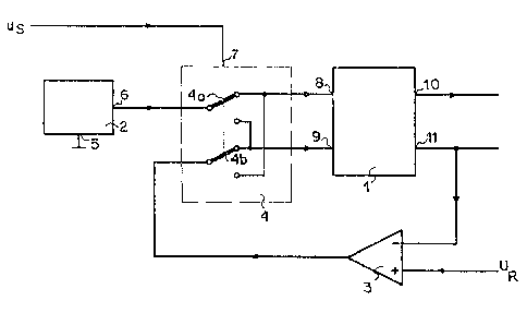
The electrical circuit of the present invention
comprises a four-pole device 1, a source 2, an amplifier 3
and a controllable two-pole selector switch 4, which has a
first switch contact 4a and a second switch contact 4b.
Source 2 is any signal source, that has two con-
nections 5 and 6. Illustratively, source 2 is a current
souxce or a voltage source. Connection 6 of the voltage
source 2 is connected to an input of the four-pole device 1
by way of the switch contact 4a. The connection 5 of source
2 is connected to ground. The amplifier 3 is for example an
operational amplifier. The selector switch 4 preferably
comprises semiconductor switches, which for example are made
using CMOS-technology. The selector switch 4 has a control
3 --
~2~S2~
input 7, and is controlled by a control voltage comprising
rectangular pulses. Illustratively, -the rectangular control
pulses are used to periodically switch the selector switch
4.
The four-pole device 1 has two input connections
8 and 9 and two output connections 10 and 11. The first
output connection 10 is a single-pole output of the elec-
trical circuit. The voltage potential of the second output
connec-tion 11 forms a base potential for the output voltage
of four-pole device 1. (This means that the voltage output
at connection 10 is measured relative to the base voltage
at connection 11). Output connection 11, which is car~ying
the base potential, is connected to an inverting input of
amplifier 3. The non-inverting input oE amplifier 3 is at a
constant reference voltage UR and the output of amplifier 3
is connected with the .input connections 8 and 9 oE four-
pole devic~ 1 b~ wa~ o~ the switch contact ~b of switch 4.
The seleckor switch ~ is used to connect the four-pole
device 1, source 2 and the amplifier 3 AS follows. In the
first position, (.i.e. .in the position shown in Figure 1,)
switch contact 4a connects connection 6 of source 2, with
the first input connection 8 of the four-pole device 1 and
switch contact ~b connects the output of amplifier 3 with
input 9 of the four-pole device 1. In the second position
of selector switch 4, connection 6 of source 2 is connected
with the second input 9 of the four-pole device 1 by way of
the first switch contact 4a, and the output of amplifier 3
is connected by way of the second selector switch contact
4b with the input connection 8 of the four-pole device 1.
Illustratively, the four-pole device 1 is an
integrated Hall element in an integrated circuit. The
inputs 8; 9 of the four-pole device 1 are then the supply
ii2:~
inputs of the Hal1 element and the outputs 10, 11 of the
four-pole device 1 are the outputs of the Hall element
be-tween which -the Hall vol-tage is created.
l'he bridge circuit shown in Figure 2 comprises
four resistors Rl, R2, R3 and R4 and shows for example the
equivalent-circuit diagram of such a Hall element. Resis-
tors Rl and R2 are serially connected, as are resistors R3
and R4.
Both series connections Rl;R2 and R3;R4, however,
are connected in parallel. The mutual connection of the
resistors Rl and R3 represents the first input connection 8,
the mutual connection of resistors R2 and R'l represents
the second input connection 9, the mutual connec-tion o:E
resisto.rs R3 and R~ repre~ent~ the Eirst output connection
10 and the mutua;L connect:ion o~ res:isto.rs Rl and R2 repre-
sents the secorlcl o~ltput conrlect:ion 11, of the Eour-pole
device L.
~ [~he amE~liEler 3 belon~s to a regulating circuit,
whose desired value is the reference volta~e UR and whose
actual value is the b,ase voltage potential at the output
connection 11. The latter is at the same time the base
potential of the output voltage of the four pole device 1
and is compensated with the help of amplifier 3, i.e.
regulated down to zero voltage. In order to achieve this,
the amplifier 3 compares the desired and the actual values
and produces at its output a voltage, which is proportional
to the difference between the desired and actual values and
which over the switch contact 4b and the four-pole device 1
counteracts the voltage potential at the output connection
11 of the four-pole 1 in such a manner, that the difference
of the desired and actual values equal zero. If this is
-- 5 --
~2~i52~4
the case, then the voltage potential of the output connec-
tion 11 equals the reference voltage UR, i.e. zero voltage,
if UR = O. However because oE the existing "offset" voltage
the reference voltage UR should be chosen not exactly, but
only tentatively at zero voltage.
Since the information containing signal that ls
produced by source 2 is reversed in polarity by switch 4
before reaching the four-pole device 1, this reversion of
polarity has no influence on the polarity of the inter-
ference component of the output voltage of the four-pole
device 1, which illustratively is produced internally in
the four-pole 1. Thus the polarity of this interference
component is in~ependent, for example, of periodical
switches of polarity of the information containing signal.
~ Finally, the above described embodiments of the
invention are intendecl to be illustrative onl~. Numerous
alternative embodiments may be devised by those skilled in
the art, without depart.in~ :Erom the spirit and scope of
the followin~ cla.ims.
-- 6
~ ,.