Note: Descriptions are shown in the official language in which they were submitted.
~2~57~
61051-1983
A FLAT ELECTRON CONTROL DEVICE UTILI~I~G A U~I~ORH
SPACE-CHARGE CLOUD OF FRE~ ELECTRONS
AS A VIRTUAL CATHODE
The present invention relates generally to flat electron
control devices and more particularly to a ~pecifically designed
flat visual display device which differs significan~ly from the
prior art.
BRIEF D~SCRIPTION OF THE DRA~INGS:
Figure 1 is a diagrammatic illustration, in side
elevation, of a flat display device designed in accordance with
the prior art;
Figure 2 is a partially broken away exploded,
perspective view of a flat visual display devlce designed in
accordance wlth one embodiment of the present lnvention;
Figure 3 is a diagrammatic illustra~ion, in side
elevation, of the device of Figure 2;
Figure 4 diagrammatically illustrates operational
aspects of the device of Figures 2 and 3; and
Figure 5 is a diagrammatic illustration, ln side
elevatlon, of a flat visual display device designed in accordance
wlth a second embodiment of the present invention.
A typical prior art approach to flat cathode ray vi~u~l
display devices i~ ~hown in Figure 1. Thi~ Figure
diagrammatically illustrates part of a prior art high vacuum
device which i~ generally indicated by the reference numeral 10.
Thi~ high vacuum devlce 10 includes a face plate as~embly 12
having a face plate 14 and an electrically positive phosphorescent
$ ~`~
. ~.. .... :
.
~ ~5574
61051-1983
coated and aluminized back face 16 (also referred to as screen or
anode) which, as a result of the impingement of electrons thereon,
provldes a visual image as viewed from front face of plate 14.
While the face plate is shown flat, it can be made slightly curved
(defining a relatively large radius) for manufacturing purposes,
as can all of the otherwise flat components making up the overall
device. This is also true for the device of the present
invention. For purposes herein, the term "flat" is intended to
include those slight curvatures. Spaced rearward of the screen
and in front of a back plate 18 and backing electrode 19 are a
series of thermionically heated wire cathodes 20 disposed in a
plane parallel with both the screen and hack plate. Each of the
cathodes is responsible for producing its own supply oi
la
iS7~
--2--
free electrons in a cloud around and along the length of
itself, as generally indicated by the individual clo~1ds
22. These free electrons are acted upon by a ~rid stack
24 comprised of addressing electrodes, a buffer elec-
trode, focusing electrodes and, in some cases, deflect-
ing means all of which will be discussed immediately
below, so as to cause the electrons acted upon to
impinge on specific areas of the the screen 16 of face
plate assembly 12 in order to produce a desired image at
front face of plate 14. For purposes of description,
the planes containing the cathodes,- screen, grid stack
and back plate will be defined by the x and y- axes and
the axis perpendicular thereto will be the z-axis.
Still referring to Figure 1, the grid stack 24 of
electrodes includes an electrically isolated buffer
electrode 25, one or more apertured address plates 26
and one or more focusing electrodes, two of which are
exemplified at 28 and 30. As an example of the address
plate 26, the latter may include a dielectric substrate
32 having a ~ront face 36, a back face 38 and closely
spaced apertures 40 extending in the z-direction between
these faces in an array of rows and columns. ~his
particular address plate illustrated also includes a
first set of parallel strip address electrodes 42
disposed on the back face of substrate 32 and a second
set of parallel strip address electrodens 44 normal to
electrodes 42 on ront ~ace 36. ~o~ p~lrposes Oe dis-
cussion, the address electrode9 42 wil.l be referred to
as the first address electrodes and the electrode strips
44 will be referred to as the second address electrodes,
as these are the closest and second closest address
electrodes to the supply of electrons. It should he
noted that while electrodes q2 are the first address
electrodes, the buffer electrode 25 is actually the
first electrode in the stack.
A-42599/SCS
D3/SCS2
~265~4
--3--
The components making up overall display device 10, as
described thus far, are conventional components and,
hence, will not be discussed in any further detail.
Also, it is to be understood that not all of the compo-
S nents making up device 10 have been illustxated. Forexample the overall de~ice includes a housing or enve-
lope which may or may not integrally incorporate face
plate 12 and back plate 18 but which nevertheless
defines an evacuated interior containing the
phosphorescent coated electrically positive screen 16,
backing electrode 19, cathode 20 and the grid stack 24
described above. The device also includes gas absorp-
tion devices such as getters to maintain high vacuum,
suitable means for energizing the cathodes 20 in order
` 15 to produce their respective clouds of free electrons 22
for providing a controlled positive unidirectional field
and means not shown for voltage biasing the various
other electrodes including placing a ~ooiti~ bias on
backing electrode 19 with respect to the cathode volt-
age, in order to act on free electrons produced by thecathodes in an attempt to cause those electrons acted
upon to move in a relatively uniform stream and with
relatively uniform z axis velocity toward the buffer
electrode. Throughout this process, the buffer elec-
trode 25 is maintained at a positive voltage relative tothe cathode voltage, thereby taking a positi~7e role in
drawing electrons to it. At the same time, means (not
shown) are provided for aAdress.ing (by app~opria~ely
voltage biasin~) selQct@d sector~ of the ~irst and
second electrodes at any given time in order to draw
electrons through specific apertures 40 and in the
direction of screen 12. Once those electrons pass
through the selected apertures, the remaining electrodes
28 and 30 (and any others if they axe provided) function
to focus or deflect or otherwise further direct the
electrons passing therethrough onto the screen.
A-42599/SCS
D3/SCS2
~26SS74
--4--
It is to be understood that device 10 has been provided
as a generalized example of some categories of the prior
art and is not intended to incorporate all of the
features of prior art devices or represent a specific
device. ~or example, other prior art devices may
utilize a different arrangement of addressing and
focusing electrodes and/or may provide different types
of individual cathodes. However, in each of the prior
art applications of the type generally illustrated in
Figure 1 (of which applicant is aware,), a spatially
non-uniform supply of free electrons ~ produced and
acted upon directly by the buffer, addressing and
focusing electrodes (and possibly deflecting electrodes)
in order to produce the desired image. In the case of
device 10, the clouds 22 of free electrons surrounding
cathodes 20 provide such a supply which is acted upon
directly by the grid stack 24.
Flat display devices exemplified by device 10 have been
found to produce visual displays which tend to vary
uncontrollably in brightness from a spatial standpoint.
There are two basic causes for this "washboarding"
effect. First, there are density variations in the free
electrons produced by and relative to the cathode wires.
More specifically, the number of free electrons ap-
proaching the grid stack immediately behind and avail-
able to one sector of the address plate might differ
from the amount behind and available to another sector.
Therefore, even if two di~ferent apertures are ~ddre9sed
for the same amount o~ time with th~ intent o~ cau9ing
the same ~umber of electrons to pass therethrough in
order to provide equally illuminated pixels on the
screen, different amounts might in fact pass through the
apertures and therefore result in pixels having entirely
different illumination intensities. The second
washboarding effect is a result of the wide angle
approach of some of the electrons being caused to move
A-42599/SCS
D3/SCS2
. ~
~6557~L
- 5 - 61051-1983
into a given aperture being addressed. These "wide angle" elec-
trons tend to pass through the particular aperture off a~is,
thereby making focusing variable.
Ideally, one way to eliminate the washboarding effect
described is to provide device 10 with a cathode 20 directly
behind and in close proximity and precisely spaced with respect to
each and every aperture 40 so that each of these apertures could
draw from similar reservoirs of electrons. In that way, if any
two or more apertures are addressed for the same amount of time,
they would under ideal conditions draw the same number of electrons
and therefore illuminate the screen with the same degree of inten-
sity. However, it should be apparent that from a practical stand-
point there are far to many apertures in the address plate to
provide an equal number of cathodes, nor could cathodes and
spacing be made precisely identical.
Another drawback of devices exemplified by device 10
resides in its use of buffer electrode 25. As stated above, this
electrode is maintained at a positive voltage relative to the
cathode voltage. As a result, the buffer electrode acts as a
constant current drain as does the backing electrode if the latter
is maintained at a positive voltage.
Exemplary devlce lO is one approach to E~a~ v.~sual
display deviccs. Arlothcr appxoach :Is illustrated in United
States Patents 4,227,117; 4,451,846; and 4,158,210. 'l'hese
patents describe devices which use a scries of focusing, deflect-
ing and accelerating electrodes working in unison to produce an
~s~
- 5a - ~1051-1983
array of individual scanning electron beams on a cooperating
electrically positive screen. While devices of this type do not
generally have washboaxding problems, they are subject to cathode
emission variations and problems associated with
iS~7~
6--
deflection distortion and borderline registration.
In still another prior art approach, electrons are pro-
duced by means of plasma. The electrons are extracted
out of a plasma generated cloud by means of an address
stack in front of the cloud and directed onto an elec-
trically positive screen. A problem with this technique
is that the light output on the screen is limited (weak)
because it is necessary to provide a very small space
between the electrically positive screen and the address
stack in order to minimize the potential on the screen.
This is because a large potential between the two would
tend to break down the gas between the grid stack and
screen creating gas breakdown therebetween. There are
also other known disadvantages to this approach.
Another category of flat display devices utilizes
single, multiple or ribbon beams directed initially
essentially parallel to the plane of the display and
then caused to change directions essentially in the Z
direction to address appropriate areas of the display
target either directly or by way of a selecting and/or
focusing grid structure. Examples are the ~iken and
Gabor devices, U. S~ patents 2,928,014 and 2,795,729,
respectively, using single guns, the RCA multibeam
channel guide system as exemplified by U. S. patents
4,103,204 and 4,103,205 and the Siemens A.G. controlled
slalom ribbon device (U.S. patent 4,437,044). The major
drawback of these systemr r~s.ide~ ln th~ con~tr~lcti(~n
and/or elect~ical and e.l@ctroll opt.ical con~rol complex-
ities.
The Siemens approach issued in U. S. patent 4,435,672 by
Heynisch utilizes a cathode region permeated by very
low velocity electrons described as having velocities of
1 to 2 volts and described variously as "electron
reservoir," "electron cloud," "cloud of low velocity
A-42599/SCS
D3~SCS2
~265~i7~
--7--
electrons," "electron storage space" and "electron gas."
The problem areas involve:
1. The ability to maintain density uniformity,
since even minor magnetic fields will disturb the
uniformity of the space charge cloud, such as those
occasioned by the earth 15 magnetic field or those
generated by curren,s in the circuitry;
2. The lack of adequate electron density due to
the relatively large volume required for the overall
cathode space; and
3. There is no reasonably fixed cathode distance
which can act as a virtual cathode for the purpose of
controlling the subsequent focusing action required to
obtain small, well defined spots at the screen.
In view of the foregoing, it is a general object of the
present invention to provide a flat high vacuum visual
display device which is not subject to the nonuniformity
or washboarding effects discussed above nor excessively
sensitive to magnetic ~ *~4~.
Another general object of the present invention~;5to
provide a flat visual display device which is energy
efficient in operation.
A more particular object of the present invention is to
provide a flat visual display device including a grid
stack incorporating address electrodes and a suppJ.y of
free electrons for use hy the addr~ @.lectr~e, ~llt
specifically a device in which th(l el.e~trode~ ~ormin~
part of the stack or any other electrodes do not draw
any appreciable current or power from the free electrons
during operation of the device.
Another particular object of the present invention is to
provide a flat visual display device of the last-
mentioned type but one in which all addressed apertures
A-42599/SCS
D3~SCS2
--8--
of its grid stack pass the same number of electrons for
a given increment of time, whereby to insure against the
nonuniformity or washboarding effect described above.
As will be described in more detail hereinafter, the
device disclosed herein includes a planar receptor, for
example a flat display screen which may be identical to
the one forming part of device 10, that is, a face plate
assembly having a front face and a coated electrically
positive back face and means on the latter which, as a
result of impingement of electrons thereon, provides a
corresponding visual image as viewed from the face
plates's front face. However, the present invention
does not require that the planar receptor be a visual
display screen. It could be, for example, an end plane
of individual electronic leads to activate other devices
such as a liquid crystal display. However, for purposes
of discussion, the receptor will be described as a
display screen and the overall device will be referred
to as flat visual display device. This device also
includes a grid stack which may be identical to stack 24
forming part of device 10 in Figure 1 or an arrangement
which only includes the apertured address plate. In
addition ancl in accordance with the present invention,
the flat visual display device disclosed herein utilizes
an arrangement including cathode means for establishing
a uniformly dense space-charge cloud of free electrons
within a planar band parallel with and just rearward of
the back side of the first addrcss gxid so that ~acll ancl
every aperture in lhe addrcss plate se~es and ac'ts upon
an equal supply o~ el~ctrons during operation of the
device.
It is furthermore a requirement that the above noted
dense planar space charge cloud form a virtual cathode,
i.e., the density of the cloud must be such that the
electric field within the cloud must at some plane
A-42599/SCS
D3/SCS2
~265~74
g
(e.g., within the band referred to above) at least drop
to cathode potential or slightly below. It is to be
clearly understood that whenever the text refers to the
phrase "space charge cloud" this re~uire~ent is includ-
ed. Also, the terms "space charge ~a~ d~" or "virtualcathode" may be used interchangeably.
In one specific embodiment illustrated herein, the
uniformly dense space-charge cloud of free electrons or
"virtual cathode" is established by means of a backing
electrode and an accelerator electrode in combination
with the previously described first address electrode of
the device's grid stack, all three acting on electrons
supplied by suitable cathode means such as cathodes 20
in Figure 1. As will be described in detail hereinaf-
ter, these three components cooperate with one anotherin order to cause free electrons emitted by the cathode
means to oscillate back and forth in a pendulum-like
fashion between two planar bands, one behind and adja-
cent to the first address electrode and one in front of
and adjacent to the backing electrode.
In the same specific embodiment illustrated herein, the
first address electrode is maintained at a bias voltage
which is at most equal or slightly negative with respect
to the cathode means during quiescence of the overall
device (e.g., when no addressing takes place). This
~nsures that, during the quiescent period, the ~pace-
charge cloud adjacent the flddr@ss plate is at all times
spatiall~y sepflrated from the first address elcctrode.
As a result, there is no current passage into that
electrode from the free electrons. I'his is to be
contrasted Wit}l device 10 in which its buffer electrode
continuously drains current from its cathode means.
Hence the device illustrated herein may be operated in a
more energy efficient manner, as will become more
apparent hereinafter.
A-42599/SCS
D3/SCS2
., .:
.. ; ~ .
~2~5~
- 9a - 61051-1983
According to a broad asp~et of the invention there is
provided a flat visual display device, comprising
(a) a flat face plate having a front face, an opposite
back face, and means on the latter which, as a result of the
impingement of electrons thereon, provides a visual image at said
front face;
(b) an arrangement including cathode means for establishing
a uniform space-charge cloud of free electrons defining a planar
band which funetions as a virtual eathode, whieh is spaeed-apart
from said cathode means and which is parallel with and rearward
of the baek face of said display faee plate, said arrangement
ineluding means other than said eathode means for eausing some
of said free electrons to oscillate back and forth more than onee
between said planar band and a second spaeed-apart loeation; and
(e) address means disposed in spaeed-apart, eonfronting
relationship with the baek faee of said faee plate between the
latter and said uniform space-eharge eloud for aeting on elee-
trons within said e:Loud in a eontrolled way so as to eause the
eleetrons aeted upon to impinge on speeifie areas of the eleetri-
eally positive sereen of said face plate in order to produee a
desired image at the front face of said faee plate.
~eeordin~ to anothor broAd ASpoCt of tllo ln~ention
there is provided a flat vi.sual dlsplay devlee, eomprising:
(a) a flat faee plate having a front face and opposite back
face eleetrieally positive means on the latter whieh, as a result
of impingement of eleetrons thereon, provides a visual image at
C
.
~2~5~i7~
- 9b - 61051-1983
said front face;
(b) cathode means for providing a supply of free electrons
in an area behind and spaced from said face plate;
(c) address means including an apertured address plate
disposed in spaced-apart, confronting relationship with the back
face of said face plate between the latter and said area contain-
ing said supply of free electrons;
(d) a backing electrode extending in a plane parallel
with and behind said area;
(e) a grid-shaped accelerator electrode e~tending in a
plane parallel with and between said address means and said back-
ing electrode within said area; and
(f) means for voltage biasing said address means and
said backing and accelerator electrodes in a way which causes
the three to act on the free electrons supplied by said cathode
means within said area to establish a uniform space-charge cloud
of free electrons defining a planar band which is spaced-apart
from said cathode means and which is parallel with and between
said address plate and accelerator grid, said planar band of
free electrons functioning as a virtual cathode which is remote
with respect to said cathode means, whereby the addr~ss plate is
able to act on electrons supp:l.lcd b~ sald v:l.rt~lal cukhode in a
controllcd way so as to aause khe ~lectrons ~cted upon to implnge
on specific areas of the back face of said face plate in order
to produce a desired image at the front face of the face plate.
~ccording to another broad aspect of the invention
C
~l265~
- 9c - 61051-1983
there is provided a flat electron control deviee, eomprising:
(a) means defining an electron receiving plane;
(b) an arrangement ineluding cathode means for establishing
a uniform space-charge cloud of free electrons defining a planar
band which functions as a virtual cathoae, whieh is spaeed-apart
from said cathode means and which is parallel with and rearward
of said receiving plane, said arrangement including means other
than said cathode means for causing some of said free electrons
to oscillate back and forth more than onee between said planar
band and a second spaced-apart location; and
(c) address means disposed in spaced-apart, eonfronting
relationship with said receiving plane between the latter and
said uniform space-charge eloud for acting on electrons within
said eloud in a eontrolled way so as to eause the eleetrons aeted
upon to be directed into specifie areas of said reeeiving plane.
Aeeording to another broad aspeet of the invention
there is provided a method of produeing a visual image on the front
faee of a flat displ.ay faee plate having said front faee and an
opposite baek faee and means on the latter whieh, as a result of
the impingement of eleetrons thereon, provide said vi.sual image
at said front faee, said method eomp.ris.Lng thQ ~te~s oE:
(a) providlng el~etron~ :Erom e~tho~o moa.ns and aeting on
said free eleetrons for establishing a uniform spaee-eharged eloud
of free eleetrons defining a planar band whieh funeti.ons AS a
virtual eathode, whieh is spaeed-apart from said eathode means,
and whieh is parallel with and rearward of the baek faee of said
~265~i7~
- 9d - 61051-1983
display face plate, said free electrons being acted upon by means
other than said cathode means such that some of the free electrons
acted upon oscillate back and forth more than once between said
planar band and a second spaced-apart location;
(b) providing address means in spaced-apart, confronting
relationshi.p with the back face of said face plate between the
latter and said uniform space-charge cloud; and
~ c) operating said address means so as to cause the latter
to act on electrons within said space-charge cloud in a controlled
way so as to cause the electrons acted upon to impinge on specific
areas of the back face of said face plate in order to produce said
image at the front face of said face plate.
According to another broad aspect of the invention
there is provided a method of controlling the flow of free elec-
trons into an electron receiving plane, comprising the steps of:
(a) providing free electrons from cathode means and acting
on said free electrons for establishing a uniform space-charge
cloud of free electrons defining a planar band which functions as
a virtual cathode, which is spaced-apart from said cathode means,
and which is parallel with and rearward of said receiving plane,
said free electrons being acted upon by means other than said
cathode means such that some of Lhe .e.~ea ~l.octrons ac~ed upon
oscillate back an~ forth mo.re than on@ b~tween sald planar band
and a second spaced-apart location; and
(b) acting on the electrons within said cloud in a con-
trolled way so as to cause the electrons act.ed upon to be directed
.,~
~;~6~iS7~
- 9e 61051-1983
into specific areas of said receiving plane.
According to another broad aspect of the invention
there is provided in a device which requires the use of free
electrons, an arrangement for supplying said free electrons, said
arrangement comprising means including cathode means for establish-
ing a uniform space-charge cloud of free electrons in the form of
a planar band at a loeation remote from said cathode means, said
planar band Gf free electrons funetioning as a virtual cathode
which is remotely located with respect to said actual eathode
means, said arrangement including means other than said cathode
means for eausing some of said free eleetrons to oseillate baek
and forth more than onee between said planar band and a seeond
spaeed-apart loeation.
According to another broad aspeet of the invention
there is provided in a flat eleetron eontrol deviee ineluding
means defining an eleetron reeeiving plane, a supply of free
eleetrons, and address means ineluding an address plate having a
plurality of spaeed-apart apertures therethrough, said address
means being disposed in spaeed-apart eonfronting relationship with
and behind said reeeiving plane and eonfigured to aet upon free
eleetrons from said supply in a eontrolled wa~ to eause the el~e-
trons aeted upon to be direeted through speelFie on~. o.E the
apertures and into speei~ie axeas o. said .r~e~ivln~ plane, the
improvement eomprising:
(a) eathode means for produeing free eleetrons at a
loeatio.n remote rom said address plate; and
- sf - 61051-1983
(b) means not including said cathode means acting on free
electrons for causing some of the electrons acted upon to oscil-
late back and forth more than once between two spaced-apart
locations for establishing space-charge clouds of free electrons
which form virtual cathodes at said locations immediately adjacent
and behind said apertures in said address plate and which serve
as said supply of free electrons to be acted upon by said
address means, each of said space-charge clouds displaying a uni-
form density of free electrons which is greater than the density
of free electrons filling the space between said clouds and
remotely located source of free electrons, at least during the
operation of said device when the supply of free electrons are not
being acted upon by said address means.
According to another broad aspect of the invention
there is provided in a flat electron control device including
means defining an electron receiving plane, a supply of free elec-
trons, and address means including an address plate having a
plurality of spaced-apart apertures therethrough, said address
means being disposecl in spaced-apart confronting relationship with
and behind said receiving plane and configured to act upon free
electrons from said supply in a controlled way to cause the elec-
trons acted upon to be directed through speciEic ones oE thc
apertures and into specific areas o:~ ~a:Ld r~ae:i.v:i.ng p~ ne, the
improvement comprislng:
(a) cathode means for producing a source of :Eree electrons
at a location .remote from said address plate; and
(li .
~l~6S~
- 9g - 61051-1983
(b) means not including said cathode means acting on
said free electrons for causing a portion of the electrons acted
upon to oscillate back and forth more than once between
(i) first locations immediately adjacent and behind
said apertures and spaced from said cathode means whereby to form
concentrated clouds of free electrons that function as remote
virtual cathodes at said first locations in order to serve as said
supply of free electrons acted upon by said address means, and
(ii) second locations further behind said apertures
whereby to form concentrated clouds of free electrons at said
second locations.
According to another broad aspect of the invention
there is provided in a method of operating a flat electron control
device including means defining an electron receiving plane, a
supply of free electrons, and address means including an address
plate having a plurality of spaced-apart apertures therethrough,
said address means being disposed in spaced-apart confronting
relationship with and behind said receiving plane and configured
to act upon free electrons from said supply in a controlled way
to cause the electrons acted upon to be directed through specific
ones of the apertures and into specific areas of said receiving
plane, the improvement comp:rlsing the BtepS of:
(a) producing .Erom cathod~ mcan~ E.ree e~eckron~ at a
location remote from said address plate; and
(b) without the aid of said cathode means, acting on said
free electrons for causing some of the electrons acted upon to
oscillate back and forth more than once between two spaced-apart
locations for establishing space-charge clouds of free electrons
C
~26S~7~
- 9h - 61051-1983
which form virtual cathodes at predetermined locations immediate-
ly adjacent and behind said apertures in said address plate and
serving as said supply of free electrons to be acted upon by said
address means, each of said spaced-ch~e clouds displaying a uni-
form density of free electrons which is greater than the density
of free electrons filling the space between said clouds and
remotely located source of free electrons, at least during the
operation of said device when the supply of free electrons are not
being acted upon by said address means.
According to another broad aspect of the invention
there is provided in a method of operating a flat electron control
device including means defining an electron receiving plane, a
supply of free electrons, and address means including an address
plate having a plurality of spaced-apart apertures therethrough,
said address means being disposed in spaced-apart confronting
relationship with and behind said receiving plane and configured
to act upon free electrons from said supply in a controlled way
to cause the electrons acted upon to be direeted through specifie
ones of said reeeiving plane, the improvement comprising the steps
of:
(a) produeing free eleetrons at a first locati.on remote
from said address plate us.ing ~uitablo me~n~ ko ~o go; and
~b) without khe ald of sald suitable means, act.ing on said
free electrons for eausing a portion of the el.ectrons acted upon
to oscillate back and forth more than onee between
(i) seeond locations immediately ad~aeent and behind
6~
~265574
- 9i - 6105~.-1983
said apertures and remote from said first loeation whereby to
form concentrated clouds of free electrons that funetion as vir-
tual eathodes at said first location in order to serve as said
supply of free eleetrons acted upon by said address means and
(ii) third locations further behind said apertures
whereby to form concentrated elouds of free electrons at said
third locations.
Aceording to another broad aspect of the invention
there is provided in a flat electron control device including
means defining an electron reeeiving plane, a supply of free elee-
trons, and means aeting on the free eleetrons in a eontrolled
manner in order to direct the electrons acted upon into said
electron receiving plane, the improvement comprising:
(a) means for produeing free electrons at a specific loca-
tion; and
(b) means acting on said free eleetrons for eausing a
portion of the eleetrons acted upon to oscillate back and forth
more than.once between
(i) a first planar band remotely loeated with respeet
to said speeific location so as to form a planar band of concen-
trated eloud of free electrons that funetions as a virtual cathode
at said fi.rst remote loeation in o.rdex to s~rva as s~ld ~upply o.E
f.ree eleetrons and
(ii) a seeond planar band remotel.y loeated relative
to said first planar band loeation so as to form a seeond eoneen-
trated planar band of free eleetrons at said seeond loeation.
~265~7~
- 9j - 61051-1983
According to another broad aspect of the invention
there is provided a method of operating a flat electron control
device including means defining an electron receiving plane, a
supply of free electrons, and means acting on the free electrons
in a controlled manner in order to direct the electrons acted upon
into said electron receiving plane, the improvement comprising the
steps of:
(a) producing a source of free electrons at a specific
location; and
(b) acting on said source of free electrons for causing a
portion of the electrons acted upon to oscillate back and forth
more than once between
(i) a first planar band remotely located with respect
to said specific location so as to form a planar band of concen-
treated cloud of free electrons that functions as a virtual
cathode at said first remote location in order to serve as said
supply of free electrons and
(ii) a second planar band remotely located relative
to said first planar band so as to form a second concentrated
planar band of free electrons at said second location.
According to another broad aspect of the inventi.on
there i.s provided i.n a hlgh vacllum dl.splay dev.Lccl whlch comp.rlses
a planar cathode~umincscent screen and pLana.r control electrode
means responsive to applied voltages for permitting passage of
el.ectrons therethrough in areas subject to external selection, the
combinatlon of: a cathode structure comprising a plurality of
~:6~;~7~
- 9k - 61051-1983
therinionically electron-emissive elements arranged substantially
within a plane; means for defining a boundary potential parallel
with and spaced behind said cathode structure; a planar accelerat-
ing electrode highly transparent to electrons and positioned
between said cathode structure and said control electrode means;
said cathode structure and said accelerating electrode being sub-
stantially parall.el to said control electrode means; said cathode
structure, said boundary potential defining means, said accelerat-
ing ~lectrode and said control electrode means jointly defining
a space in which electrons are trapped and forced to oscillate
back and forth between two regions of high electron density, the
first being near the boundary potential derining means, the second
being adjacent and parallel to said control electrcde means and
constituting a virtual cathode which is remote from said cathode
structure and from which electrons may be drawn to the screen as
commanded by the control electrode means.
According to another broad aspect of the invention
there is provided in a high volume electron control device which
includes planar control electrode means responsive to applied
voltages for permitting passage of electrons therethrough in areas
subject to external selection, the combination o~: cathodc means
for provid.tng a supply Oe Eree elcctrons w.LthLn a g:l.ven planc
spaced behind said planar control electrode; means definlng a
boundary potential parallel with and spaced from said given plane;
a planar accelerating electrode hlghly transparent to electrons
and positioned between said given plane and said control electrode
jr ~ ~9
~55~
- 91 - 61051-1983
means; said given plane and said accelerating electrode being sub-
stantially parallel to said control electrode means; said boundary
potential defining means, said accelerating electrode and said
control electrode means jointly defining a space in which said free
electrons are trapped and forced to oscillate back and forth
between two regions of high electron density, the first being
adjacent said boundary potential defining means, the second being
adjacent and paral]el to said control electrode means and con-
stituting a virtual cathode which is remote from said cathode
means and from which electrons may be drawn to the screen as
commanded by the control electrode means.
According to another broad aspect of the invention
there is provided in a flat el.ectron control device including
means defining an electron receiving plane, a supply of free elec
trons, and address means disposed in spaced-apart confronting
relationship with and behind said receiving plane and configured
to act upon free electrons from said supply in a controlled way to
cause the electrons acted upon to be directed into specific areas
of said receiving plane, the improvement comprising:
(a) first means at a location remote from said address
plate for providing free electrons during operation of said control
device; and
(b) secon~ means ~epa'rel'te .E.rom .sa.l.d fl.~s~ mcan~ actlncJ
on said f:ree electrons for causing a porti.on of the electrons
acted upon to oscillate back and fo:rth between
(i) a first location immediately adjacent and behind
~65574
- 9m - 61051-1983
said apertures whereby to form a concentrated cloud of free elec-
trons at said first locations in order to serve as said supply
of free electrons acted upon by said address means, and
(ii) a second location further behind said apertures
whereby to form a concentrated cloud of free electrons at said
second locations;
(c) said second means being configured such that, for any
particular group of free electrons supplied by said first means
at any given point in time, at least some of the electrons from
that group will oscillate back and forth between said locations
a number of times.
According to another broad aspect of the invention
there is provided in a method of operating a flat electron control
device including means defining an electron receiving plane, a
supply of free electrons, and address means disposed in spaced-
apart confronting relationship with and behind said receiving
plane and configured to act upon free electrons from said supply
in a controlled way to cause the electrons acted upon to be
directed into specific areas of said receiving plane, the improve-
ment comprising the steps of:
(a) using cathode means, providing free electrons at a
location remote from said add~ess p:l.ar.~ ~urlny op~ra~.lon oE sald
control device; and
(b) acting on said source of free electrons without the aid
of said cathode means for causing a portion of the electrons acted
upon to oscillate bac~ and forth between
. .
~S~74
- 9n - 61051-1983
(i) a first location immediately ad~acent and behind
said apertures whereby to form a concentrated cloud of free
electrons at said first locations in order to serve as said free
electrons acted upon by said address means and
(ii) a second location further behind said apertures
whereby to form a concentrated cloud of free electrons at said
second location;
(c) said step of acting on said electrons being such that,
for any particular group of free electrons qupplied by said
cathode means at any given point in time, at least some of those
electrons from that group will oscillate back and forth between
said locations a number of times.
~;~6S574
61051-1983
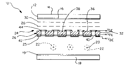
Turni.ng now to the drawings, wherein like components are
designated by like reference numerals throughout the various
Figures, attention is immediately directed to Figures 2 and 3, as
Figure 1 has been discussed previously. Figure 2 illustrates a
flat visual display device which is designed in accordance with
the present invention and which is generally indicated by the
reference numeral 46. This device may include the same face plate
assembly 12 (or other such planar receptor~, back plate 18,
cathodes 20, and apertured address plate 26, as described
previously with respect to device 10 illustrated in Figure 1. The
apertured address plate 26 is located dlrectly behlnd and in
parallel relationship wlth the phosphorescent coated and
a].uminized back face
B lo
~265574
--11--
16 of face plate assembly 12. The addressing electrodes
42 are shown extending in one direction on the back face
38 of the address plate's substrate 32 and second
addressing electrodes 44 extend in normal directions on
the opposite side of the address plate. The apertures
40 in the address plate are illustrated in both Figures
2 and 3.
Note that device 46 does not necessarily include or at
least does not have to include (although it may include)
additional focusing, deflecting and/or addressing
electrodes between the address plate and screen corres-
ponding to focusing electrodes 28 and 30 and other such
electrodes which may make up the grid stack 24 in device
10. Also note that the wire-like cathodes in device 46
run parallel to G1 electrodes 42 rather than perpendicu-
lar to these electrodes, as in device 10 This has been
done for purposes of illustration and has no significant
effect on the operation of overall device 46. The
cathodes could run in either direction. Finally, it
should be noted that device 46 has an outer most enve-
lope which, while not shown in its entirety, includes
face plate 14 and back plate 18 and defines an evacuated
chamber containing the phosphorescent screen 16 of the
display face plate, wire-like cathodes 20 and address
plate 26 as well as other components to be discussed
hereinafter.
In addition to the components thus ~ar descrlbefl,
overall ~Iat visu~l displ~y device 46 includes a plate
like backing electrode 50 located behind cathodes 20 in
a plane adjacent to and parallel with ~and possibly
supported by) backing plate 18 and a grid-shaped accel-
erator electrode 52 disposed within a plane parallel
with and between address plate 26 and cathode wires 20.
The way in which these two additional components operate
in device 46 will be described hereinafter. For the
A-42599/SCS
D3/SCS2
~:'
~. ..
~2~5~i74
-12-
moment it suffices to say that these two additional
components in combination with those described previous-
ly establish a first uniformly dense space-charge cloud
or virtual cathode 54 of free electrons in a planar band
(e.g., a flat layer having thickness) disposed in
parallel relationship with and immediately behind the
first address electrodes 42 and a second uniformly dense
space-charge cloud 56 of free el~ctrons in a planar band
in parallel relationship with and immediately in front
of backing electrode 50. As will be seen, space-charge
cloud 54 is essential to the operation of device 46
while space-charge cloud 56 is a result of the way in
which the space-charge clouds are established and is not
otherwise essential to the operation of the device.
Therefore, all discussions henceforth will be directed
primarily to space-charge cloud 54, although it will be
understood that the space-charge cloud 56 includes
identical attributes.
From the way in which space-charge cloud 54 is estab-
lished, as will be described, it will be apparent that
this reservoir of free electrons has essentially zero
forward and rearward z-axis velocities te.g., in the
direction noxmal to the plane of address plate 26) and a
random Maxwellian cross beam velocity (parallel to the
plane of the address plate) and thus the electric field
at any point within the cloud is essentially zero.
Stated another way, each and every point or sub-area
within space-charge cloud 5~ at a g.tven plan~r di~tance
from the first addres~ electrode 42 include~ essentially
the same density of free electrons d.isplaying the same
essentially zero field conditions as each and every
other point or sub-area. In that way, "virtual cath-
odes" which are identical to one another are established
at each and every aperture 40 immediatsly behind ad-
dressing electrodes ~2. As electrons are drawn from
these virtual cathodes by the apertures during the
A-42599/SCS
D3/SCS2
~2~5S7~
-13-
addressing mode of the device, the voids they leave are
immediately filled so as to preserve the uniformity of
the overall cloud, provided the number of electrons
emitted is well in excess of the current which is drawn
by the grid stack and accelerator electrode as will be
discussed. This is because the cloud 54 is made to be
sufficiently dense, in the manner to be described
hereinafter, as compared to the number of free electrons
drawn to the addressed aperture, so that addressing the
cloud by the aperture has minimal effect on the cloud's
field. When electrons are drawn from the cloud, the
tendency of~ cloud to maintain equilibrium causes an
instant redistribution in which electrons in the immedi-
ate surroundings move in to fill the void. This assures
that each aperture has a continuous supply of electrons
to draw from and that each supply is the same as the
other.
Having described space-charge cloud 54 and before
describing how this cloud is established, attention is
directed to the way it is utilized in combination with
addressing plate 26 for directing controlled beams of
electrons from the cloud through selected apertures 40
and on to screen 16 in order to produce a desired visual
image on the latter. To this end, certain nomenclature
should be noted. Specifically, those apertures which
are energized or addressed are ones which are caused to
direct electrons from cloud 54 towards screen 16. On
the other hand, those apertur~s wh.ich are not ~norgiz~d
or addressed are maintain@d electronic~llly cl~sed to the
passage o~ electrons.
Whether any specific aperture is addressed or not
depends upon the voltages on ~he particular first and
second addressing electrodes 42 and 44 which orthogon-
ally cross that aperture. In the case where no aper-
tures are being addressed, that is, during the quiescent
A-42599/SCS
D3/SCS2
,:"' '
.:
,
,, " .
~6S~7~
- 14 - 61051-1983
mode, the first addressing electrodes are maintained (biased) at
a voltage at most equal or slightly negative with respect to
cathodes 20 while the second address electrodes are also main-
tained at zero or a negative cutoff voltage. Thus, in the case
where no apertures are being addressed, none of the electrons from
cloud 54 are attracted to the address plate and thus there is no
current drained by either of the address electrodes and hence no
power is consumed. This is to be distinguished from device 10
where there is continuous current drain in the grid stack through
the buffer electrode 25 which is always maintained at a positive
voltage with respect to its cathodes ~0.
If a buffer electrode is used in the stack the first
address electrode does not necessarily have to be zero or negative
but it must be such that in combination with the buffer no current
will flow into the grid stack past the first address electrode.
In some cases a slight amount of positive voltage on the buffer
which will not consume a large amount of power may be of advan-
tage as a means of producing focusing.
The precise "cutoff" voltages on each set of address
grids must be adjusted so that no current due to field penetra-
tion will flow as a result of the turn-on pulse volta~c of Ph~
other. If a buef~r clect,rocte :L~ us~d L~ ~ont, o~ the ~irst
address electroctes, as wlll be descri.bed wi.th respect to Fi~ure 5,
then the combination field establlshed with the latter must
function the same as the first address electrode without the
presence o~ a buffer.
~26~57~
~ 14a - 61051-1983
In order to energize or address a particular aperture,
its specific first and second address electrode must both be
energized to voltage level.s positive with respect to the cathode
potential. For purposes
C
~26~is7g
-15-
herein, it is to be understood that the cathode poten-
tial or the cathode reference voltage is its unipoten-
tial value during the addressing mode of the overall
device. If cathodes 20 are directly heated structures,
then there must be a non-addressing mode or period in
order to heat up the cathodes. During this non address-
ing mode of the device, the cathode potential must be
zero or positive with respect to the first addressin~
electrode at all points. If the cathodes are/~heate~,
then there is no need for a non-addressing mode.
Because the first address electrode associated with the
specific aperture being addressed during the address
mode is increased to a voltage above that of the cath-
ode, there will be a certain amount of power consumed as
a result of electrons attracted to ~b}e~ the rest of
the energized first address electrode from cloud 54.
However, the resulting current drain is negligible due
to the fact that only a relatively small number of
pixels are simultaneously addressed such as for example
those in a single or a double line or column along the
first address electrode and therefore the power loss is
negligible.
Having described space-charge cloud 54 and the way in
which address plate 26 is operated, attention is now
directed to Figure 4 which illustrates how the space-
charge cloud 5~ is established. It will be assumed at
the outset that the entire a~re~ plate 26 i~ in a
quiescent mofle, that i~, ea~h o~ its apertures rernains
in an unaddressed state. t1nder this condition, the
first address electrode voltage ~indicated at VFE)
remains at its cut off value equal or slightly negative
with respect to the cathode voltage Vk. As stated
previously, the voltage on the second address electrode
(indicated at Vse) is maintained at cutoff. At the same
time, the backing electrode 50 is maintained at a
voltage VBE which is close to VFE, that is equal or
A-42599/SCS
D3/SCS2
~265~7~
-16-
slightly negative with respect to the cathode voltage
Vk. With the specific cathode system shown and for
specific spacing it may at times be advisable to operate
the backing electrode very slightly positive in order to
increase cathode emission without however absorbing
appreciable current in comparison to the increased
emission. On the other hand, the voltage Vacc on
accelerator electrode 52 is maintained at a positive
level with respect to the cathode voltage ana both VFE
and VBE.
It should also be noted that the device must be so
constructed that the side wall in the regions aft of the
grid structure are at backing electrode potential. This
will enclose the free electrons within the confines of
the back plate side walls, and grid stack during quies-
cent operation, and the accelerator will therefore be
the only current collector.
Under the voltage biasing conditions just recited, as
electrons are emitted from wire-like cathodes ~0, they
will be drawn from the cathode toward the accelerator
electrode and a percentage thereof will actually be
intercepted by the accelerator mesh in some finite time
period. Due to inertia, the remainder will move through
the mesh-li~e accelerator electrode toward first address
electrodes 42. The fraction of electrons not intercept-
ed by the accelerator grid will be roughly eq~lal to the
transmission characteristic o~ thc gricl, which ~or
purposes o~ discussiorl will b~ ~s~umed to be approxi-
mately 95%. This means that e~ch time a given number of
electrons are attracted towaxds the accelerator plate,
95% will pass therethrough and 5~ will not~ As stated
above, the first address electrodes are biased at a
voltage level equal to or slightly negative with respect
to the cathode voltage. Accordingly, repulsive forces
are created between these electrodes and the oncoming
A-42599/SCS
D3/SCS2
~65~i74
-17-
electrons, thereby slowing down the latter and eventual-
ly causing them to momentarily stop and be repelled back
towards the accelerator electrode. Upon returning to
the accelerator mesh, a fraction of those electrons, for
example 5~, will be intercepted by the accelerator while
the others pass therethrough and move toward the backing
electrode. Since the backing electrode is at the same
voltage as the first address electrode, the oncoming
electrons will be turned back towards the accelerator
electrode and the process will repeat itself in a
pendulum like manner.
The action just described is diagrammatically illustrat-
ed by the overlapping waveforms 60 in Figure 4. Note
that the electrons bunch in planar bands parallel with
and adjacent to the first address and backing electrodes
as their velocities go to zero in the direction normal
to the accelerator electrode (e.g., in the Z-direction).
The velocities of the electrons go to zero at slightly
different distances from the first address and backing
electrodes, thereby partially accounting for the thick-
ness of the bands. This is because the electrons are
emitted from the cathode at different thermal veloc-
ities, ~within a relatively tight range) and therefore
approach the electrodes at slightly different energies.
As a result they tend to bunch within the bands so
defined, thereby resulting in the previously described
space-charge clouds 54 and 56. At the same time, the
electrons forming the clouds tend to move in r.lndom
directions paral.l.el with th~ aecQlerator ~lectrode
(e.g., in the x alld y directions). ~owever, the space-
charge fields in these latter directions tend to cancel
themselves out, thereby resulting in a space charge
cloud effectively having a zero field in all directions,
as discussed previously.
It should be apparent from the foregoing that the
A-42599/SCS
D3/SCS2
~26S574
-18-
proximal region of space-charge clouds 54 and 56 with
respect to the first address electrode and backing
electrode 50 respectively, depend in large part on the
voltage values on these latter electrodes and that o~
the accelerator electrode. ~dditionally, the proximal
regions of the space charge clouds from the accelerator
grid are essentially functions of the current density
passing through the accelerator grid and the voltage of
the accelerator grid. The value of this dimension can
be assessed from the Child Langmuir equation for a
planar diode
2 3/2
J = a V
X 2
where "J" is the current density passing through the
accelerator
"a2" is a a constant equal to 2,335 x lO 6 amperes per
volt
"Vacc" is the accelerator voltage
is ~ ximately the zero potential boundary of the
space for given values of the above current and
voltages neglecting thermal velocity
3/4
Restated, xO = a Vacc in unit distance
J~
I'he same also holds for the sp.~cc between th~ accelera-
tor and the backplate assuming that the cathode struc-
ture is not present. This of course requires a design
somewhat different from the given example.
~'~te rl t ~
If the f~ at the first electrode (either the first
address electrode or a buffer electrode) in the grid
A-42599~SCS
D3/SCS2
~2~557~
--19--
~le~
stack is i~ equal to cathode potential then the
electron velocities in the space between xO and the
first grid stack element will be essentially thermal in
the z direction as well as in the xy plane.
Negative values will result in a linear negative gradi-
ent which will cause the proximal boundary of the space
charge to the grid stack to be pushed back and cause the
virtual cathode band (e.g. the space charge cloud) to be
pushed away from the grid and the space charge will
become narrower and denser. This will tend to increase
the need for higher voltages in the addressing con-
ditions of the first address grid or the combination of
address grid and buffer ~lectrode.
A slightly positive value at the stack entrance will
cause the Child Langmuir law to become effective in the
xO-to-stack region with the stack entrance voltage now
being entered in the equation and xO being the distance
from the potential minimum, to the stack entrance.
From the above discussion and the desire to keep power
levels low and pulse amplitudes at a minimum, for
obvious reasons, then the design functions must be
adjusted so that
1. Vacc be reasonably low
2. The density of electrons adjacent to the stack
be high
3. xO distance from th~ ~ccQl~x~tor be ~reat~r
than that from t.h0 ~rid structure
Compromises for purposes of focusing can of course be
made as noted before.
It should be noted that a virtual cathode or uniform
space charge cloud will always exist provided that
A-42599/SCS
D3/SCS2
12~5~7~
-20-
emission current is greater than the current absorbed by
the grid structure and the target or screen. Typical
values of voltages and other param~ters are for example
VBE = OV
Vacc = 15 to 20 V
Stack entrance field (quiescent) close to OV
Accelerator to grid stack spacings = .070
Cathode emission~ =~ma/in2 of display area
B
In the way of a simple restatement the following should
be noted.
An object of the invention is to be able to adjust the
position of the cloud 54 with respect to the address
plate 26 in order to adjust the focusing and intensity
or brightness capabilities of the overall device. Also,
by placing the cloud as close as possible to the first
addressing electrode, the amount of energy required to
draw electrons into and through given apertures being
addressed is minimized. At the same time "cross talk"
between apertures is also minimized. This means that
electrons are drawn through one aperture being addressed
and not adjacent ones unaddressed and will not influence
the display status (brightness and/or focus) of adjacent
apertures.
One way to insure that the space-charye cloud 5~ .is as
close as pos~ible to the first Adelres~ electrodes is to
posit.ion the ~ccelerator elec~rode as close ~s possible
to the first address electrodes, while, at the same
time, maintaining VFE as close as possible but negative
with respect to the cathode voltage Vk. In this way,
the space-charge cloud is forced into a small dense band
width between the two. In this latter regard, the
accelerator electrode should not be so close to the
first address electrode so as to shadow approaching
A-42599/SCS
D3/SCS2
~265S7~
1051-1983
electrons. At the same time, it is desirable to minimi~e the
spaclng between cathodes 20 and the accelerator electrode in the
specific design noted so that the voltage on the accelerator can
be maintained at a minimum level to provide a given emission
current. The closer the accelerator electrode is to the cathod~s,
the lower the voltage need be for a given current. Thus, by
minimizing the voltage at a given current (by minimizing the
cathode/accelerator spacing), the energy consumed can be
minimized. While still referring to the positional relationship
of the cathodes and accelerator electrode, the latter is
preferably between the cathodes and address plate 26 as illustra-
ted. However, for the design described here the accelerator
electrode could be located on the opposite side of the cathodes
as well. More specifically, referring to Figure 4, because
of the evident symmetry of space-charge clouds 54 and 56, the
positions of the cathode and accelerator electrode can be
interchanged.
In actual practice, a typical address plate is
subjected to both line and column addressing. Depending upon
the application of overall device 46, the :~irst address
electrodes wlll be used :Eor line or co.lumn ad~re~:l.ncJ a~cl the
second address eloctrotlos will be used in the opposlte WAy.
If the stack structure is not u~ed as a storage system then the
device is best operated as a line or column sequential system.
that is to say that if line sequential. addressing is used then
the ~irst address electrode is turned on sequentia].ly one line at
a time and all columns are addressed simultaneously for each
line. Thus the grid stack and screen combination tends to
-21-
~265~i7~
1051-1983
absorb closely the same fraction of the cathode current and
therefore aid in maintaining display brightness and focus
uniformity. In the case column sequential addressing the
columns are sequentially addressed on the first control grid and
all lines are addressed simultaneously on the second control
~rid. If the columns or line array which are addressed simul-
taneously are split then two lines or columns respectively can
be addressed on the first address electrode at an increased
trade-off of brightness or line or column count.
The purpose of addressing a potential grid-like
buffer electrode 52 as shown in device 46 of Figure 5 to the
grid stack at the input side of the grid stack provides a
means of controlling the space charge for the purpose of
focus adjustment or to maintain a near zero entrance field to
the stack should :it be necessary to use a negative or perhaps
positive first selection electrode to produce a proper cut-off
level at this electrode. This latter device 46', except for
its buffer electrode 62, is identical to device 46 and includes
all of the components described above along with the buffer
electrode. This latter electrode is operated at a voltage
so that the entrance potential to the grid stack is zero or
slightly negative with respect to the oakhode vo:Ltage ~lc~ ~n
that way, the spa~e-cha~ge cLo~l~l 5~ ~ e~tab.Lishecl ju~t rearward
o the buer electrode.
In either device 46 or device 46', the means for pro-
viding a supply oE Eree electrons was described as parallel
-22-
~26557~
1051-1983
cathode wires and the accelerator electrode was described
as grid-shaped. It is to be understood that these and the
other components making up device 46 or 46' could vary in
design without departing from the spirit of the invention.
For example, the cathodes do not have to be in the form of
parallel cathode wires or wires at all so long as a suitable
supply of electrons are provided at the appropriate location
within the device to establish the desired space-charge cloud~
~~ " -23-