Note: Descriptions are shown in the official language in which they were submitted.
i5~
ELECTRONIC POSTAGE METER OPERATING 9YSTEM
Field oE the Invention
The present invention is directed to nonvolatile memory
systems, and more particularly, nonvolatile memory sy~tem3 for
electronic postage meters.
Back~round o~ the Invention
Postage meters are mass produced devices for printing a
defined unit value for governmental or private carrier delivery
of paxcels and envelope~. The term postage meter also includes
other like devices which provide unit value printing such as
tax stamp meters. Postage meters incIude internal accounting
device~ which account for postage value representation which
is stored within the meter. The accounting device accounts
for both the recharging of the metPr with additional postage
value and the printing of po~tage by the meter printing
mechanism, No external independent accounting system is
available for accountiGg for the postage printed by the meter.
~ ~ :
; ~ ,.
t,. ~r r.
.
-- 2
Accordingly, postage meters must possess a high reliability
to avoid the 105s of user or governmental funds stored within
the meter and dispensed by printing postage.
Electronic postage meters have been developed and are
disclosed, for example, in U.S. Patent No. 3,978,457 for
MICROCOMPUTERIZED ~LECTRONIC POSTAGE METER SYSTEM; in U.S.
Pat~nt No. 4,301,507 for ELECTRON:IC POSTAGE METER HAVING PLURAL
COMPUTING SYSTEMS; and, in U.S. Patent No. 4,484,307, for
ELECTRONIC POSTAGE METER HAVING IMPROVED SECURITY AND FAULT
TOLER~NCE FEATURES. Such meters have electronic accounting
circuits which include electronic non-volatile memory
capability for ~toring postage accounting in~ormationO ~he
accounting circuits and associated postage printing mechanism
are physically sealed within a tamper resistant enclosure.
The non-volatile memories are provided for storing critical
postage accounting information when external operating power
is not applied to the meter.
Various types of accounting information may be stored in
the meter non-volatile memory. This information includes, for
examplë, the total amount of postage remaining in the meter
for subsequent printing ~descending register) and the total
amount of postage printed by the meter (ascending register).
Other types of accounting or operating data may also be stored.
For example~ service information in the form of error codes
denoting various types of malfunctions or abnormal conditions
encountered during operation of the meter may be stored in
non-volatile memories. This facilitates the evaluation of the
operating experience of each meter to assist in its repair,
should that be necessary, and to accumulate data helpful in
the design of electronic postage meters.
Non-volatile memories as well as the other electronic
accounting circuitry within electronic postage meters are
susceptible to disturbances which can either destroy
information or cause erroneous information to be generated.
The electronic circuits are susceptible to electromagnetic
radiation and electrical transients which can interfere with
the proper operation of the meter and accurate storage of
information. These types of effects can result in a 105s of
funds to the users and, accordlngly, it has been
recognized that various types oE protection must be
provided to avoid such undesirable results as the data
cannot be reconstructed in most instances from other
externally available records.
Electronic postage meters of the type that write to
nonvolatile memories only during power down se~uence
such as disclosed in above identified U.S. Patent
4,301,507, operates satisfactorily for their intended
purposes. However, if a difficulty occurs during the
several milliseconds when external power is removed and
the capacitance within the system provides the power to
write, critical accounting information may be lost.
This information may not be able to be reconstructed
because it is not stored in other nonvolatile memories.
Systems have also been developed, such as disclosed
in U.S. Patent No. 4,484,307 for ELECTRONIC POSTAGE
METER HAVING IMPROVED SECURITY AND F'AULT TOLERANCE
FEATURES which have memories wherein data is written
into nonvolatile memories during each operation of the
meter.
Summary of the Invention
It has been discovered that electronic systems such
as described above can be improved by an improved
circuit and software arrangement.
The organization of the system is such that
information is written into nonvolatile memories, under
predetermined operating conditions and in a manner which
enhances the reliability of the system.
5;~ P'.~
-- 4 --
A postage meter system in accordance with the pre~ent
invention includes nonvolatile memory means and program store
means coupled to a mlcrocomputer means. Postage meter
transactional accounting data records are stored in the
5nonvolatile memory~ Each transactional accounting data record
include~ a header portion having piece count related data and
a piece count data field. The mo~t current s~ored transactional
accounting record header includes piece count related data
which difers from the piece count data stored in the piece
10count field. Other stored tranr,actional accounting records
have headers with piece count re:Lated data which are the same
as the piece count data stored in the piece count Eield. In
this way, the most current record can be rapidly identified~
In accordance with the present invention nonvolatile
15memory locations are utilized for storing postage value setting
prior to the commencement of a postage dispensing transaction.
By utilizing the ring buffer postage setting data and the most
current postage transactional accounting record a postage meter
transaction can be reconstructed and written into a new postage
20transactional accounting record should a writing into
nonvolatile memory fault occur during the concurrence of a
postage meter transaction and the powering down of the postage
meter system.
In accordance with another feature of the present
25invention, a random access memory means and program store mean~
are coupled to the microcomputer means. The program store
means causes the microcomputer means to write a full set of
critical postage accounting data into the random access memory,
a second full set of critical accounting data and a set of
30abbreviated critical accounting data into the nonvolatile
memory. The program store means further causes the
microcomputer means, when an error is detected in at least one
of the nonvolatile memory records, upon a compari~on of data,
where data in the random access memory is used as the accurate
35reference data, to rewrite data into both the full record and
the abbreviated data record stored in the nonvolatile memory.
4a
Other aspects of this invention are as follows:
In a postage meter system of the type including a
microcomputer means, nonvolatile memory means, and
program store means, the improvement comprising: said
nonvolatile memory means having locations for storing
postage meter transactional accounting data records;
each transactional accounting data record having a
header portion including piece count related data and a
piece count data field, one of said locations having
stored thereat a most current stored transactional
accounting record including a most current stored
transactional accounting record header; the most current
stored transactional accounting record header including
piece count related data which differs from the piece
count data stored in the piece count field; and, wherein
others of said locations store transactional accounting
records having headers with piece count related data
which is the same as the piece count data stored in the
piece count field such that the most current stored
~ransactional accounting record can be rapidly
identified.
A postage meter system comprising:
a microcomputer means;
nonvolatile memory means;
random access memory means; and,
program store means including means to cause said
microcomputer means to write at least three records
including a first full set of critical postage
accounting data into locations in the random access
memory, a second full set of critical accounting data
into the nonvolatile memory means and a third set of
abbreviated critical accounting data into said
nonvolatile memory;
said program store means further including means
responsive to an error detected in at least one of the
sets of data in said location in said non-volatile
memory to cause said microcomputer means, upon a
comparison of data in said random access memory and said
~2~
nonvolatile memory where said data in the random access
memory is used as the accurate reference data, to
rewrite data into both the full set of critical
accounting data stored in the nonvolatile memory and
the abbreviated cri-tical accounting data stored in the
nonvolatile memory.
Bri~ D~~E~tion of Drawinqs
Figure 1 is a simp].ified perspective view of a
postal meter showing a slmplified diagram of a circuit
for the accounting system of the meter in accordance
with the invention;
Figure 2 is a schematic of the manner in which
Figs. 2a, 2b, 2c, 2d, 2e and 2f interconnect to one
another for showing the detailed schematic circuit
diagram of the accounting sys~em shown in Figure 1;
Figure 2a is a detailed schematic diagram showing
input circuitry for the microprocessor of the
accounting system shown in Fig. 1;
Figure 2b is a detailed schematic diagram showing
the microprocessor and some of the output circuitry,
including an address latch, of the accounting system
shown in Fig. 1;
Figure 2c is a detailed schematic diagram showing
additional output circuitry of the accounting system
shown in Fig. 1, including a PROM and a non-volatile
memory;
Figure 2d is a detailed schematic diagram of
further circuitry of the accounting system shown in Fig.
1, including another non-volatile memory;
Figure 2e is a detailed schematic diagram of still
further circuitry of the accounting system shown in Fig.
1, including output circuitry for coupling the
microprocessor of Fig. 2b to the printer;
Figure 2f is a detailed schematic diagram of yet
further circuitry of the accounting system shown in Fig.
1, including circuitry for coupling the microprocessor
of Fig. 2b to the lift interposer and circuitry for
5Q
coupling a minus 30 Volt d.c. supply to the
microprocessor shown in Flg. 2b;
Figure 3 is a is a schematic diagram showing the
manner in which the details of flow charts of Figs. 3a
and 3b are interconnected to each other for showing the
detailed circuitry o~ the accounting module main line
loop;
Figure 3a is a portion of the flow chart referred
to in Fig. 3;
10Figure 3b is the remainder of the flow chart shown
in Fig. 3;
Figure 4 is a flow chart showing the accounting
module trip processing;
Figure 5 is a flow chart showing the nonvolatile
memory block write routine;
Fi~ure 6 is a flow chart showing the power down
processing routine;
Figure 7 is a schematic diagram showing the manner
in which the detailed circuit showing the load normal
block data routine are indicated;
Figure 7a is a portion of the flow chart showing
the routine of Fig. 7;
Figure 7b is the remainder of the flow chart
showing the routine of Fig. 7;
25Figure 8 is a flow chart showing the load service
block data from the MNOS or EEPROM memories;
Figure 9 is a flow chart showing computing trip
record address routine;
Figure 10 is a flow chart showing find current trip
record routine;
Figure 11 is a flow chart showing read first
portion of current primary trip record routine;
Figure 12 is a flow chart showing the trip record
verification routine;
35Figure 13 is a flow chart showing trip record error
logging routine;
Figure 1~ is a flow chart showing set postage on
print wheels routine;
~i5~
Figure 15 is a flow chart showing find current
postage record routlne;
Figure 16 is a flow chart showing repair trip
record routine;
Figure 17 is a flow chart showing open nonvolatile
memory block routine; and,
Figure 18 is a flow chart showing update
nonvolatile memory block routine.
f J~`
- .1'':,`
~v~ .
-- 6 --
Detailed Description of the Preferred Embodiment
Circuit Architecture Overview
In the present sy~tem both a floating gate EEPROM type
nonvolatile memory and an MNOS type nonvolatile memory are
employed in conjunction with a microprocessor having a random
access volatlle memory. The random access memory, as in the
present system, may reside on the integrated circuit chip which
contain~ the microprocessor. The system is designed 50 that
information from the microproce~3sor is both written into the
random access memory and into the EEPROM memory on a
transactional basis. The information is written into both the
EEPROM memory and the MNOS nonvolatile memory during a power
down routine. Additionally, writing can occur to both the
EEPROM nonvolatile memory and the MNOS memory duriny block
switching times, as for example, when the service mode switch
is moved from the operating position to the service mode
position.
A uni~ue ~ystem o interleaving the writing between the
EEPROM memory and the MNOS memory enables the data to be written
into both memories during power down without extending the
period of time necessary to write into either of the memories
individually. This greatly enhances the reliability and
security of the meter without additionally providing further
risks that information may be lost during power down.
The writing techni~ue is such that the writing is
interleaved. That is, a byte of information is first written
into the EEPROM memory. Since it takes two milliseconds for
the information to be written into the EEPROM memory locations
after the data is put on the EEPROM memory data line ports,
this time period is uqed for writing two nibbles of data into
the MNOS memory. This memory is nibble oriented and the writing
time takes one millisecond per nibble. Thus, during the wait
period while the data is being written into the EEPROM
nonvolatile me~ory the same data iQ simultaneously beingwritten
into the MNOS type nonvolatile memory. The interleaving
continues until both memories are fully loaded with the relevant
data necessary to be stored during a power down se~uence.
-- 7 --
The above writing sequence for the particular design
involved may take approximately 60 to 70 milli~econd~ while
the power from the capacitance store which is available for
continued operation of khe meter after a power failure is
detected is in the range of 200 milliseconds.
As a further protection because of the necessity for the
particular circuit disclosed to output a 16 bit address at port
2 of the microprocessor, here an 8051 type microprocessor,
when writing to the EEPROM nonvolatile memory, and since the
M~OS memory is also connected to port 2 of the 8051
microprocessor, the addressing scheme Eor the EEPROM memory
has been selected such that the data line~ coupled to the M~OS
memory always are at a high, or one value, whenever the EEPROM
memory is addressed for the purpose of either writing or
reading. This is of a particular importance in protecting the
data in the MNOS memory because of the manner ln which writing
must occur in this memory. It shoul~ be noted that to write
into the MNOS nonvolatile memory it is necessary to ~irst erase
the 4 bit locations to be written into~ To achieve this, it
is necessary to write ones (1) into each of the memory locations
and this must be done for a period of time of approximately
10 milliseconds to erase the location and therefore enable a
later write to occur. As a result of this arrangement for the
data input, the data lines of the MNOS memory are connected in
a unique manner, specifically, to different pins o the same
port as the high order address lines of the EEPROM memory.
With the data lines of the MNOS memory held high for a
period of approximately 2 milliseconds when the E~PROM memory
is being addressed, the MNOS memory is put into a condition
wherein inadvertent writing into memory location is prevented.
This is because should the write enable line inadvertently be
activated during this period of time, the memory locations with
a 1 in them would not change since a 1 is being written in~ On
the other hand memory locations with a 0 would also not be
changed because they had not previously been erased and made a
1 to enable the writing step to occur. Additionally, the
erasing process cannot occur because it takes approximately
$
-- 8 --
lO milliseconds to erase a location to ~nable the memory
location to be written into and the EEPROM addressing timing
is only 2 milli~econds.
As a further feature of the present organization it should
be noted that the circuit org2lnization and architecture is
such that minimal lines are shared between the EEPROM
nonvolatile memory and the MNOS nonvolatile memory. This
provides a highdegree of"separation" anda level ofprotection.
Physically, the two memory devices share only lO I/O lines of
the microcontroller. For the MNOS memoryt all 10 ~hared lines
are used only for latching the addres~. The control lines such
as chip enable, read enable, write enable, and the like, are
totally separated between the two chips. Such separation can
help in reducing any possible mutual interference.
Software Archltecture _verview
The software operating the system and the memory mapping
arrangement for storing data, particularly in theEEPROM memory,
provide a high degree of redundancy hither to unavailable in
previous electronic poqtage meters. It has been discovered
that by organizing the real time accounting into two sets of
20 records in the ~EPROM memory ln a unique manner, additional
reliability can be achieved. Firstly, in the unlikely event
a particular memory component i9 unavailable, the software
architecture has been established qo that it can function with
either the nonvolatile MNOS nonvolatile memory pr~sent or
removed from the system. Moreover, the addressing technique
for writing into the EEPROM memory has eliminated the need ~or
a separate pointer used in previous designs. Specifically,
it has been discovered that data from the piece counter can
3 a be used in the header of the r~cords stored in the EEPROM
memory as a logisal record pointer indicating where the record
should be written after a trip has occurred. In the particular
embodiment disclosed, it is the last, least significant 5 bits
of the piece counter which provides the logical pointer for
the record into which the data should be written.
Moreover, it has been discovered by placing the piece
counting data into the header of each record quick
identification can be achieved of the most current record
- 9 -
stored in the EEPROM memory without the necessity, as in
previous systems, of writing header location information twice
per trip, once to indicate new records and once to indicate
old records. Moreover, the techni~ue allows the rapid acces~
of desired records by a technique which permits a quick search
and identification of desired information. The organization
of the memory is such that there are two sets of twenty records
stored in the EEPROM memory. When the meter i5 put into
sarvice, the memory locations are initialized so that proper
data is stored in all memory locations. The usa of the piece
count data in the header of each record ~et allows a quick
indication of both the oldest and the most curr~nt tprevious)
records stored. The most current stored record includes the
oldest piece count number which i~ updated only after a trip
has been completed.
In the above manner, in conjunction with information
concerning the setting of the postage value in a ring buffer
stored in nonvolatile memory, which data is stored prior to
the commencement of a trip, should any malfunction occur
reconstruction using the ring buffer postage setting data and
the mo~t current tprevious~ record allows a recovery from the
fault by using the postage value ring buffer setting to update
records. This avoids the necessity to pull meters out of
service due to the inability to recover from a single "bad
trip~. That is, a meter operation where data concerning the
trip is not accurately recorded. As an additional feature in
the memory organization, error counter inormation is
maintained for a number of separate error conditions. This
allows enhanced analysis of failure and fault condition~ which
may occur in the meter wh n the memory contents are read and
analyzed.
It should be noted that the two sets of twenty records
are designed so that the primary record has full data. That
is the record contain~ a nonvolatile memory write ~oft error
counter or pointer to remap record; a closing coun~er twrite
on next trip); a piece counter; a ~RC of descending register;
descending register; CRC of ascending register; ascending
register; CRC of data from the byte 2 to byte 10 hex, this
-- 10 --
provides a CRC for insuring that the critical data i~ correct;
postage value setting; batch amount; batch count; PIN number
(for parcel registers only); printer statu~ when trip bit is
cleared, i.e. this hyte is written only when the trip is
completed; and, lastly, a CRC from data from bytes 2 to byte
lC hex which is the CRC of the entiire record. In sharp contrast,
the back up trip record contains abbreviated information of
critical accounting data specifically the information stored
from byte 2 to byte 11 hex mentioned above. Additionally, as
a technique for providing enhanced security a nonvolatile
memory write soft error counter or pointer to a remapped record
is written in the backup record although not at the time of
tha transaction or trip~ It is an error counter which is
written into only when an error is detected and written lnto
memory. This is the same case for the main record.
The software functions such that th~ accounting
microprocessor verifies critical data o both trip records
stored in the EEPROM and rewrites them if necessary.
Specifically, after a trip is completed the current critical
data resides in three locations in the meter. A first set of
critical data is stored in the microprocessor RAM, a second
full set of critical data is stored in the EEPROM memory and
a third set of abbreviated critical data is stored also in the
EEPROM memory. If upon the comparison (wherein the data in
the RAM is used as the accurate reference data) an error is
detected, a rewrite step occurs. That is~ data is rewritten
into the EEPROM memory and thereafter compared to insure it
matches the data stored in the RAM~ This is done both for the
full record stored in the E~PROM and the abbreviated data
stored in the EEPROM. It should be noted that the full record
of the EEPROM memory is not compared; only the critical data
portion of the full record is compared. If, after an error in
the critical data is detected and a rewriting process has
occurred successfully, a soft error counter i~ incremented to
note the difflculty encountered in writing into the EEPROM
memory.
Another major feature of the so~tware is the remapping
of the trip record. Specifically the EEPROM memory is organized
such that there are 8 record locations saved in reserve That
is 4 record locations for the maLn full record and 4 record
locations for the abbreviated record. These locations are
normally not utilized in the operation of the meter. In the
unlikely event a primary record location for either the full
data or the abbreviated data occurs which can be a hardware
failure such as a memory cell failure and the like, the system
is designed to activate an unused set of record locations.
This is done in conjunction wit:h a pointing technique which
remaps the primary location to the new activated secondary
location. Thus, the reserve secondary location functions in
the capacity of the primary location when this occurs. Thi~
all occurs under software control and this error condition i~
noted by the soft error counter for the particular record
location exceeding its maximum, which in the present inskance
is 9, or a rewrite aktempt falls. Thus, a write fails and the
second rewrite attempt additionally fails.
The software is further organized to allow an infrequent
error or transient condition to occur and continue the meter
in service, however, if the transient error occurs more
frequently, the meter is permanently lock out. For example,
if the microprocessor jumps inadvertently for some reason to
an unused or spare location the meter will continue in service
if such does not happen too frequently, for example only once
every 10,000 meter trip cycles. Other errors can be treated
in the same manner. This allows segregation of meters which
have a severe but very transient error and those which have a
severe but more frequent error which should be removed from
service and corrected by setting a flag in the nonvolatile
memory such that even i the error condition is removed the
meter cannot be initialized by power dswn and power up.
Additional features are provided in the software system
to enable an access to descending register stored in the
no~volatile memory locations from the keyboard and the ability
to dump the contents o the transactional EEPROM memory without
taking the meter out of service by an external device which
communicates with the meter.
Reference is now made to the drawings wherein like
reference numerals designate similar elements in the various
views~
t~ ~_ 6
- 12 -
Circuit Operation
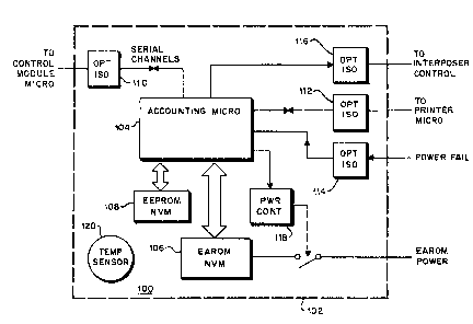
Reference i~ now made to Figure 1. An alternate form of
an accounting control system for a postal meter is disclosed
from that shown in Figure 5 of U.S. Patent No. 4,301,507 noted
hereinabove. The accounting system 100 includes an enclosure
102, the walls of which may be fornned to provide electromagnetic
shielding. The circuits within the enclosure 102 include an
accounting microcomputer 104 operatively connected to two
nonvolatile memorie~. The first nonvolatile memory 106 is an
EAROM MNOS type nonvolatile memory. The ~econd nonvolatile
memory 108 is an EEPROM nonvolatile memory. Nonvolatile memory
106 may, for example be an ER3400 manufactured by General
Instruments Corporation, Hicksville, New York and described
in i'EAROM" published November 1977 by General Instruments
Corporation and in Bulletin 1203A, "Using the ER3400" published
by General Instruments Corporation. The ~econd nonvolatile
memory 108 may be a floatlng gate electrically era~able
programmable read only memory~ as for example, part number
DE5516A manuEactuxed by SEEQ Technology Incorporated, San Jose
California and de~cribed in ~2816A/55l6A TimerE2 16K Electrical
Erasable ROMs", Preliminary Data Sheet, published February
1984 by SEEQ Technology Incorporated, San Jose, California.
The accountin~ microcomputer 104 controls the application
of stored data to the two nonvolatile memories 106 and 108 in
accordance with the present invention. The accounting micro-
computer 104 includes a random access memory which includes
working ascending registers, working descending registers and
the like. The accounting microco~puter 104 al~o includes a
read only memory control for the necessary routine~ which will
be described in greater detail hereinafter.
The accounting system 100 incorporates a serial interface,
to enable interfacing with the printing and control modules
disclosed in the above noted U.S. Patent No. 4,301,507. The
microcomputer, may for example, comprise an 8051, 8052 or 8751
type series microcomputer ~rom Intel Corporation, Santa Clara~
California. In order to avoid damage to the accounting system
100 by electrical surges applied accidentally or intentionallyt
and to eliminate electrical noise induced via ground loop~,
- 13 -
the accounting microcomputer 104 communicates with the devices
external of the compartment 102 by sui-table isolators that are
not capable of applying voltage sur~es to the microcomputer.
These isolators may, for examp:Le, be in the form of opto-
electronic couplers, and are also preferably arranged ~o as tobe inaccessible from the exterior oE the postal meter. One
isolator unit 110 may be provided for the two way co~munication
path with the control unit. ~ further isolator arrangement
112 may be provided for the tWlD way communication with the
printer unit. A still further isolator 114 may be provided
for applying the power sen3ing signal to the microcomputer
104. In addition, an isolator 116 may be provided for
controlling an interposer in the printer Eor mechanically
blocking functions of the printer.
The purpose of the power control circuit 118 i~ to provide
power to the system to enable a data transfer operation during
power down oparations to be completed when a2ternal power
fails. The program of th~ microcomputing unit 104 is organi~ed
to enter the content~ of the registers of the microcomputer
and, as appropriate to random access memory, into the
nonvolatile memories 106 and 108 as soon as an indication of
failure o~ the power supply occurs, and to restore this data
to the working registers upon restoration of power as will be
more fully e~plained hereinafter.
The enclosure 102 may urther include a temperature sensor
120, with sui~able circuits, not shown, so that the micro-
computer will operate to transfer data to the nonvolatile
memory in the event of excess temperatures by entering a power
ailure mode if the temperature is above or below predetermined
limits, as for example, 70c or 0c, respectively.
The system may prevent the operation of the meter
interposer solenoid, not shown, by way of the isolator 116,
in the event of excessive temperatures. It will be appreciated
that the interposer is controlled by the microcamputer 104
also to inhibit operation of the printer in the event that
insufficient postage remains for a printing operation, or other
accounting dat:a indicates that the meter should not he
operative.
While the isolators have been indicated as indiv
idual units, it is, of course, apparent that these units
may incorporate multiple devices, so that two way comm-
unication is established in the respective circuits.
Reference is now made to Figure 2. The accounting
microcomputer 104 is connected to the two nonvolatile
memories 106 and 108. The address ports of the EEPROM
nonvolatile memory 108 are connected to the micro-
computer 104 b~ way of an address latch 122. The
higher order address ports A8, ~9 and A10 are coupled
directly to port 2 of the microcomputer 104. The data
lines of the nonvolatile memory 108 are connected
directly to the port "0" of the microcomputer 104 and
additionally to an external PROM 124. The PROM 124 can
serve as an extra program memory capability for the
meters accounting circuit or alternatively as the source
of a diagnostic program for testing faults or failures
of the meter. The MNOS nonvolatile memory 106 address
lines ~0 through A7 are directly connected to the
microcomputer 104 por-t 0. The higher order address bits
A8 and A9 are connected to port 2 of the microcomputer
104. The four byte data input/output ports D0 through
D3 are directly coupled to port 2 of the microcomputer.
The nonvolatile memory 106 has two control lines C0
~5 and Cl which establish the operation to be performed,
namely, read, write, or erase; a write enable port; and,
a chip enable port. The two ports are connected to the
higher order 2 pins of the port 1 of the microcomputer
104. The control lines C0 and Cl are operated from port
1 of the microcomputer 104 by means of a block erase
inhibit circuit 126. The address and data lines of the
nonvolatile memory 106 are connected to the +5 volt
power supply by a series of pull up resistors 128 and
130 respectively. The pull up resistors in conjunction
with the +5 volt power supply insure that the hish level
voltage at each port is above a predetermined level,
such as -~3.6 volts, so that the high level is above the
specifiecl threshold for the device.
~6~
- 15 -
The nonvolatile memory 108 includes three control
terminal~, a chip enable terminal, a write enable terminal,
and an output enable terminal which are coupled to the micro-
computer 104. The chip enable and write enable line are
connected to the microcomputer through a circuit which includes
two negative logic AND gates 132 and 134. Each of these gate~
will provide a low output upon the occurrence of two low inputs
at their respect two input terminals. The devices 132 and 134
opera~e in conjunction with an NPN transistor 136 to protect
the contents of the nonvolatile memory 103 upon the detection
of the power fail of the operating voltage for the system.
This circuitry operates in conjunction with circuitry within
the nonvolatile memory to ensure that the nonvolatile memory
108 is in a known condition. When the operating voltage of
the circuit falls below a predetermined level, but is yet above
the level of voltage needed to cause the onboard protection
circuitry of the memory 108 to become active ~hich is 3 volt~,
the circuitry including devices 132, 134, and 136 provide
suitable protection for the memory 108.
A negative AND gate 138 is provided or manufacturing
testing purpose. One of the inputs to the gate 138 is connected
to ground by a resistor to render the gate 138 essentially
inoperative. When it is coupled to a high voltage, the negative
ANDgate 138 functions to disable the device 124 data lines by
rendering the output enable terminal of the device high.
A power fail and reset logic circuit 140 is providedO
This circuitry functions to hold the microprocessor 104 in the
reset mode until the voltages h~ve risen sufficiently and
stabilized. Additionally, on a power down occurrence when
power fail is detected, the circuit functions to both insure
that the reset signal is held off until an interrupt routine
is initiated and completed. Thereafter, the circuit functions
to insure positive application of a reset signal and the
continued application of that signal as the power falls.
As power rises, and before the power rises to the level
where it is stabili~ed, no current flows through the photodiode
142 of the opto-isolator 144. Thus, the opto-isolator outpwt
photo-transistor 146 is nonconductive. As a result, the output
- 16 -
o~ the opto-isolator L~ maintained at a high level by the
rising voltage at the ~5 volt supply. This results in a
hysteresis buffer 148 providing a high voltage output causing
the ~AND gate 150 to maintain an active signal on the interrupt
texminal of the microcomputer 104. This causes no ackivity
by the microprocessor because, as will be moxe explained below,
the microprocessor is being maintained in the reset mode which
overrides the interrupt signal. The high voltage at the output
of the hysteresis buffer 148 is applied via a reaistor 152 to
back bias a diode 154 coupled to the base electrode of PNP
transistor 156. Thi~ causes transistor 156 to be biased out
of conduction which in turn cause~ NPN transistor 158 to be
biaqed out of conduction. As a result, the reset terminal
follows thevoltageat the+5 volt power supply and is maintained
active as power rises.
When power rises to a sufficient level and stabilizes,
current begins to flow through the photodiode 142 and
phototransistor 146 i~ biased into conduction Thi~ causes
the input voltage to the hystere is buffer 148 to go low and
its output, likewise, to go low. As a result, transistor 156
is biased into conduction causing transistor 158 to al~o be
biased into conduction. This removes the reset signal from
the microcomputer 104 and simultaneously removes the active
interrupt signal applied by NAND gate 150.
When the phototransistor 146 is rendered nonconductive
due either to a power fail detection signal which causes current
to cease flowing through the photodiode 142 or a failure of
the -30 volts applied causing the supply to rise toward groundg
the interrupt line is rendered active. Thiq occurs because
the hysteresis buffer 148 has a high input applied resulting in
a high output being applied to the NAND gate 1500 As a
consequence, a low output signal applied on the interrupt line
and the microcomputer 104 under program control goes into an
interrupt power down routine.
The microcomputer begins to operafe under program control
after the operating voltages reach their proper level and
stabilize. The microcomputer continues to operate and execute
main line meter program functions until a power fail occurs
- 17 -
in either the input to the photodiode 142 where current ceases
to flow or by a failure in the -30 volt supply coupled via the
zener diode 160 to the emitter electrode of transi~tor 146.
Either a failure of the power detect circuit or a rising voltage
on the -30 volt supply cau~es phototransistor 146 to be biased
out of condu~tion, biasing diode 154 out of conduction.
Neverthele~s, under program control, an NPN transi3tor 162 is
maintained conductive until the nece~sary power down sequence
has been completed. This occur~ by having the emitter electrode
of the tran~istor 162 connected through a resi~tor 164 to
port 33. Transistor 156 continues -to be maintained
in conduction byconnecting the base electrode to ground through
the collector emitter current path of tran~istor 162 and port
33 cf the microcomputer 104. TranYistor 158 is maintained in
conduction until the power down routine iR completed and the
voltage at port 33 goeq high biasing transi~tor 162 out of
conduction. W~en thi~ occur~, tran~i~tor 156 is biased out
of conduction. A~ a result, tran~istor 158 i~ bia~ed out of
conduction and the reset signal is applied on the re~et line.
The microcomputer 104 goe~ into the reset mode and remain~ in
the mode as power falls.
A sequence control circuit 166 i~ provided for controlling
the seguence of applicatio~ of operating voltages to the MNOS
memory 106. The MNOS memory, to properly operate, re~uires
the equenced application of three æeparate ~oltage~. Thi~
is controlled by the ~equence control circuit 166. On power up,
a +5 volt operating voltage is applied to MNOS terminal 22,
not shown. It hould be noted that ~he +5 volts i9 applied to
all of the variou3 device3 a~ ~he VeC and i3 not ~hown on the
schematic circuit diagram as ~uch. The +5 volt i3 generated
when the power to the ~y3tem i~ turned on. Thereafter, a -12
volt is applied to MNOS memory 106 pin 2 Vdd. The -12 volts
i~ applied by microcomputer 104 under software control.
Specifically, port 30 goe3 low bia~ing PNP tran~istor 168 into
conduction. As the voltage rise~ on the tran~istor collector
electrode, a MOS FET transi~tor 170 is biased into conduction.
As a result the -12 volts applied to the MOS F~T ~ource electrode
L.6
is coupled via the device channel to the memory 106 terminal 2.
A re~i~tor 172 connect~ the terminal 2 to ground to provide a
static discharge path and protect the device.
When the sy~tem is turned on, and while the -12 volts i~
being established at terminal 2 of memory 106, a MOS field FET
transistor 174 having its gate electrode connected to micro-
computer port 31~ i5 biased into conduction by the ~5 volts
applied via resistor 176 to it~ gate electrode. As a result,
PNP transi~tor 178 is biased into conduction and a +5 volts
is applied to memory 106 terminal 1, Vgg. Thi~ i~ because the
ER3400 device requires the application of a +5 or a -30 vol'c~
on thi~ particular terminal to avoid an undefined condition
within the device which could adversely affect the memory
operation, such as latch up which would prevent accessing
memory locations. When the -12 volt~ has been applied to the
MNOS nonvolatile memory 106 terminal 2, the +5 volt~ i~ removed
from port 31 by microcomputer 104 causing port 31 to go
low. The program control of microcomputer 104 will allow port
31 to change from its high condition to it~ low condition only
after certain routine~ are completed to in3ure that it is
desired to effectuate a write operation to M~OS nonvolatile
memory 106 to change a memory location content. When thi~
condition occur~, a~ previously noted, port 31 goes low which
biases MOS F~T tran~i~tor 174 out of cvnduction, cau ing PNP
transistor 178 to be bia~ed out of conduction and thereby
removing the application of the ~5 voltg from the memory
terminal 1. Simultaneously, a MOS FET transistor 180 is biasad
out of conduction which in turn bia~es a PNP transi~tor 182
into conduction~ When tran~istor 182 i~ rendered conductive,
it in turn biases a MO5 FET tran~i~tor 184 into conduction
which re~ults in the applieation of a -30 volts through the
drain source electrode channel to MNOS nonvolatile memory 106
terminal 1. When this sequence has been completed, the
microcomputer 104 is able to acces~ and write into memory
locations ~ithin the nonvolatile memory 106.
After a write operation has been completed, the port 31
i~ put in a high state and the FET MOS 184 is biased out of
conduction removing the -30 volt and the PNP transi~tor 178
- 19 --
is biased into conduction applying the ~5 volts to the terminal
19 Resistor~ 186 and 187 in conjunction with capacitor 188
coupled -to tranQistor 178, and resistor 190 and capacitor 192
coupled to transistor 182 function to provide a hysteresis
effect. The values of these components are selected such that
both devices cannot be operative to apply voltages to the
terminal at the same time. ~hus, each device goes off removing
its respective voltage from terminal 1 beEore the other device
turns on to apply its voltage to terminal 1.
Communications between the printer microcomputer, control
module micxocomputer and interposer are by means of optical
isolators in conjunction with a hysteresis buffer. Thus, the
opto-isolator 116 i5 coupled by hysteresis b~ffer 194 to port
12 of microcomputer 104. It should be noted that this is a one
way serial communication channel from the microcomputer 104
to the interposer control. The control module communications
to the microcomputer is by way of opto-isolator 110R and
hysteresis buffer 196 to the T0 terminal of microcomputer 104.
Control module communications from microcomputer 104 is by way
of hysteresis buffer 198 and opto-isolator 110T. Finally,
communications from the printer microcomputer is by way of
opto-isolator 112R and hysteresis buffer 200 with communica
tions from microcomputer 104 to the printer microcomputer by
way of hysteresis buffer 201 connected to port 11 and opto-
isolator 112T~
It should be noted that the low order pins of microcomputer
104 port 2 are connected to the high order addres~ pins of
both nonvolatile MNOS memory 106 and EEPROM memory 108. The
higher order pins o~ port 2 are used as the data ports of
microcomputer 104 for nonvolatile memory MNOS 106. When the
EEPROM 108 is accessed for writing or reading purposes, the
microcomputer 104 must output a 16 bit address~ the software
selects the address of the E~PROM memory 108 in such a way
that the data input pins of the memory 106 are at 2 high level.
Consequently, i~ noise inadvertently occurs on the control
lines Swrite ~_nable, ch;p enable, C0 and Cl) whîch would
otherwise condition memory M~OS 106 to have data written into
it, the memory is still protected against overwriting because
- 20 -
writing a 1 to a 0 in the ER3400 type nonvolatile memory would
not enable an overwriting of the data into a 1. For those
locations where a 1 exists already, the writing has no effect.
Additionally, because of the particular architecture of
the present system, a high degree of isolation exists between
the circuitry employed for reading and writing into each of
the nonvolatile memorles 106 ancl 108. Specifically, only 10
address lines are shared between the two nonvolatlle memories
106 and 108. Namely, microcomputer 104 port 0 terminals P00
through P07 are shared by devices by memories 106 and 108 as
well as external program memory 124. Additionally, port 2
terminals P20 and 21 (address A8 and 9) are connected to the
high order address pins of the three memory devices 106, 108
and 124. Additionally in port 2, terminals All, 12, 13, and
14 are connected to the data lines of nonvolatile memory 106.
Finally, port 2 terminal A15 is coupled to control the chip
enable lines of device~ 108 and 124.
It should expre~sly be noted that when program from
external program mQmory 124 is being utilized to control
operation of the microcomputer 104 the particular systems
conigura~ion provides maximum protection for nonvolatile
memory 106 in a manner similar to that provided when operating
nonvolatile memory 108.
As will be further explained in connection with the
description of the flow charts, the access to the nonvolatile
memories 106 and108 is accomplished bydifferentmicroprocessor
instructions. The access to the MNOS nonvolatile memory 106
is by input/output mapping technique~. In contrast, access
to tha EEPROM nonvolatile memory 108 is by memory mapping
technique~. By utilizing two different accessing techniques
which flows from the particular hardware architecture configu-
ration rather than the inherent addressing and accessing
techniques of the device themselves, further protection is
provided against inadvertently accessing the wrong memory or
a wrong address while executing rewrite instructions to a
particular memory. Thus, it should be recog~i%ed that the two
memories are not each accessed, as for example, by memory
mapping each having different range~ where an inadvertent use
$
- 21 -
of address in the wrong ranye could cause access to the wrong
memory. Agaln, both memories are not accessed by input/output
mapping where again a wrong input or output address instruction
could access a wrong memory. This i9 because memory mapping
access instructions activate microcomputer 104 write lines and
read line ~terminals 16 and 17). However these lines are
connected only to EEPROM nonvo.Latile memory 108 and not to
MNOS memory 106. The I/O map instructions are efectuated by
the high order pins of port 1 of microcomputer 104 (terminals
5, 6, 7, and 8) which are only connected to the nonvolatile
memory 106~
Postage Meter Sequence of Operation
Figures 3 through 18 are flow charts representing the
sequence of operation of the postage meter accounting system
100.
Reference is made to Figure 3, the accounting module main
line loop. The flow chart depicts operation of the accounting
unit 100 after the power up routine has ~een completed. It
reflects the regular operation of the accounting module. It
should be particularly noted that the operation involves
receiving and processing the printer status and, in response
thereto wxiting two trip records to the EEPROM memory 108.
Additionally, when this occurs it sets a trip flag. When tha
operation of the microprocessor 104 is caused to loop back to
~he main line program loop and continues its processing it
will reach a decision block concerning whether the trip flag
has been set. If the trip flag has been set, it clears the
flag and verifies/rewrite the trip records. Specifically, it
verifies that the trip record was written correctly and if not
correctly written, attempts to rewrite the data into the memory
locations. It should be noted that the MNOS memory 106 is
written into only during power down (see Figure 18).
Additionally, the MNOS nonvolatile memory 106 is updated during
a switching of the postage meter between its normal and service
mode, should that occur.
Reference is now made to Figure 4, the accounting module
trip processing. The flow chart depicts the manner in which
the writing to the EEPROM nonvolatile memory 108 is achieved.
~ ~'$~
- 22 -
When a postage imprint or diqpensation is detected, the
accounting microprocessor 104 performs, under the program
control, the following tasks. It writes the right most two
digits of the unlncremented piece count tcount of the number
of pieces processed during an operation of the meter) as a
"header" to "close" the previous transaction record. It also
sets the trip Elag in the meter status~ Additionally, the
microcomputer 104 updates the accounting data in the micro~
processor RAM and p~rforms a cont:rol sum test. The control sum
is the sum of the ascending regLster and descending register
of the postage meter which should equal the control sum.
Additionally, the microcomputer 104 writes portion of the
current logical transaction record, which includes the piece
count, the CRC of the descending register and the descending
register value. A partial CRC Eor thedata string isaccumulated
and stored in a temporary RAM location. The microcomputer 104
under program control sends the accounting complete message
to the printer module. It further writes the CRC of the
ascending register, the ascending register value and the CRC
of the data xtring from the piece count to the ascending
register. It goes to receive and process the new status if
the printer module raises the request to send signal. The
communications protocol or the various modules i~ described
fully in the above noted U.S. Patent No. 4,301,507
The microcomputer 104 writes to the current transa~tion
record the postage value, batch amount, batch count and PIN
(parcel identification number~, if it is a parcel register
rather than postage meter. It continues accumulating the data
string CRC.
The pxogram causes the microcomputer 104 to save the last
memory address of the primary full trip record onto the stack.
It proceeds to write the back up (or abbreviated) trip record in
a byte by byte manner so that a request to send from the printer
can be served immediately. After writing the back up trip
record, the microcomputer 104 waits until the trip bit in the
printer status is cleared, then retrieves, ~pops) the memory
address of the primary trip record from the stack and writes
the new printer status and the CRC for the data string of the
- 23 -
entire primary trip record. The microcomputer 104 checks the
home position change and the synchronization between the home
position and the piece count for an error code condition. This
is to determine if the meter is operating properly. The
microcomputer sets a trip flag whLch effectively requests later
trip record verification. It then sends the meter status with
trip completed bit set to the control unit. The trip bit will
be cleared if the outgoing transmission i~ succes~ful. After
this is achieved, the program would return to themainline loop.
It should be noted that the postage value stored in each
primary trip record i~ used only for reconstructing the postage
fund in case a catastrophic memory failure occurs and the meter
is taken ou-t of service. It is used by the service department
in analyzing the data dumped from a returned meter. During
the power-up loading onto the temporary RAM, the postage value
read from the primary trip record is overwritten by the postage
setting value read from the postage ring buffer which always
contains the current postage setting value. Thus, if the
setting value is changed after a trip, the current setting
rather than the last trip setting i~ loaded into the
microcomputer random access memory.
Reference is now made to Figure 5, the nonvolatile memory
block write routine. The routine is called when it is ~esired
to write into a block of the EEPROM nonvolatile memory 106 and
MNOS nonvolatile memory 108. This occurs only during the power
down of the module or when the meter mode is switched from the
normal mode to the service mode by actuation of the service
switch disclosed in U.S. Patent No. 4,301,507. It should be
noted that the program cause~ the microcomputer 104 to write
one data byte to the EEPROM nonvolatile memory 106 without
waiting. It immediately writes two nibbles or four bit~ to
the MNOS nonvolatile memory 108 with wait and check, that is,
to read back and v~rify that the data desired to be written
into the memory locations has in fact been written.
Since a power down interruption can occur at any time, it
is possible that it ~ay be required to write information into
both nonvolatile memories 106 and 108 ~hould a power interrup-
tion occur. To a~oid the possibility that a write operation
- 24 -
has occurred within the prior two milllseconds into the EEPROM
nonvolatile memory 106~ the nonvolatile ~emory block write
routine has been arranged such that writing to the EEPROM
nonvolatile memory 106 does not occur until the proces~ing
loop has operated Eor at least two milliseconds. Thus, the
first write data to the ~EPROM nonvolatile memory 106 occurs
only after the writing of the header to MNOS nonvolatile memory
108. Since this is a two nibble header it takes more than two
milliseconds to accomplish the ~write cycle.
Reference is nowmade to Figure 6, the powerdown processing
routine. The routine shows the processing of the accounting
unit 10Q when a power down situation is encountered. It should
be noted that when the nonvolatile memory blocks are completely
written the routine turns on the connection between the power
fail and reset circuitry to the microcomputer 104 by causing
microcomputer port 33 to go low to operate the circuitry as
previously described,
Reference is now made to Figure 7, the load normal block
data routine. The routine describes the operation of the
microcomputerl04 to transfer the data stored in the nonvolatile
memories into the microcomputer randcm access memory. This
occurs during the power up of the accounting unit 100. It
should be noted that the source of data for the random access
memory comes from several lo~ations. The data comes from the
normal block data in the MNOS memory 108 it also comes ~rom
the current EEPROM nonvolatile memory 106 normal block data
and lastly, it comes from the current trip record data frvm
the EEPROM nonvolatile memory 106. It should be noted that
the data obtained from these three locations are compared to
make sure that they are consistent. If the data is not
consistent an error message is provided which causes the power
up routine to be aborted. Until the condition is resolved the
meter will not enable and cannot be utilized.
Reference is now made to Figure 8, the load service block
data from MNOS or EEPROM memories. The service block data
contains service and other meter related data needed to operate
the meter such as the higb dollar unlock, low postage warning
and other similar types of inormation. The loading of the
- 25 -
service block data operates in a manner similar to the loading
of the normal block data; however, the comparison routines are
not implemented due to the fact that this data is not as
critical to meter operation as is the basic normal accounting
information concerning postal funding.
Reference is now made to Figure 9, the computing trip
record address routine. This routine computes the trip record
address for the EEPROM nonvolatile memory 108 ~o that the
microcomputer 104 will write each trip into the properlocation.
Reference is now made to Figure 10, the find current trip
record routine. This routine provides the abillty to locate
the current trip record rapidly during the power up process
or responding to a request of the descending register stored
in the EEPROM nonvolatile memory 108. Normally, the current
trip record has the highest piece count value. Instead of
comparing the 8 digit piece count value among the 20 trip
records retained in the nor.volatile memory 108, the routine
compares the ~header" against the least significant two digits
of the piece count for each of the 20 trip records. The trip
record headers were written in real time by the accounting
module trip processing routine previously discussed for Figure
4. For the non-current trip records, the header value is equal
to the piece count value modulo lQ0. For ths current trip
record, the header value is different by 20. This is because
the header has not been updated and it still has the piece
count value (modulo 100) of 20 transactions ago. Note that
the current trip record is not identifiad by a header of a
particular fixed value. In a fixed value header scheme, it
is necessary to write the header twice, once when the record
is current and secondly to change it to a different value to
indicate that it is no longer current. This would cause the
header locations to wear out before other data area in the
nonvolatile memory with limited writ~ cycle endurance. The
technique described above avoids the difficulty.
Reference is now made to Figure 11, read first portion
of primary trip record routine. The routine is used to insure
that the real time trip record is consistent wi-th the normal
block data stored during power up routine.
-- 26 --
Reference i5 now made to Figure 12, trip record verifica-
tion routine. This routine verifies the accuracy of the
critical portions of the primary and back up trip record. The
critical portions are the piece count ascending and descending
register values. If it is determined upon the verlfication
that a trip record is bad an attempt is made t~ rewrite the
data into the same location. ;tf this fails, the record i~
rendered inoperative and a naw record is written in another
location reserved for such contingencies. The location of the
record i5 remapped to the reserved locations. The remapping
can also occur even if the rewriting to the original location
is successEul but the number of attempts to achieve the correct
data write is more than a predetermined number such as nine
attempts~
Refer~nce is DOW made to Figure 13, trip record error
logging routine. The routine detarmines whether a remap
operation is necessary and sets a remap flag in the fir~t
nibble of the record to be remapped7 It further provides an
indication to where this record will be placed in memory.
Reference is now made to Figure 14, set postage on print
wheels routine. The routine provides a real time writing into
the E~PROM nonvolatile memory 106 of the value to which the
postage meter printing mechanism is set prior to actually
tripping the meter. Specifically, the writing into this memory
location occurs prior to enabling the meter for printing, that
is, prior to the time at which the interposer is lifted so
that the shutter bar of the me~er printing meehanism can be
operated to allow the printing mechanism to be caused to print.
Thus, even if the power down interrupt routine malfunctions
in some way, data is stored in the nonvolatile memory of the
value to which the print wheels or other printing mechanism
is set prior to commencement of the printing operation and
accounting can be achieved on the next power up routine. The
routine provides a protection against multiple failures in the
sy~tem which could cause a loss of accounting data.
Reference is now made to Figure 15, find current postage
record routine. The routine controls the microcomputer 104
during power wp to find the current postage setting record
~2~ 6
- 27 -
last written before the meter became inoperativedue for example
to a power failure or to turning oEf the meter.
Reference is now made to Figure 16, repair trip record
routine. If one cannot locate the current transaction record,
5that would indicate ~hat there is some contamination of the
header data and the piece count field. In such an event, the
microprocessor under control of this sub-routine takes the
regular normal power down block oE piece count data to
reconstruct the last record localtion for the EEPROM 108 trip
10record. It is done in a manner such that all twenty headers of
the transaction records are rewritten to insure integrity of
the repaired trip records. This routine can also be utilized
when the serial number is locked into the meter after
manu~acturing and testing to set the piece counter to zero.
15Reference is now made to Figure 17, open ~onvolatile
memory block routine. The program controls the use of a back
up for emergency service block in the EEPROM nonvolatile memory
108. It is updated whenever a new MNOS nonvolatile memory
block is open, and it can be uploaded if the regular service
20blocks in both nonvolatile memories 108 and 106 are lost or
contaminated.
Reference is now made to Figure 18, update nonvolatile
memory block routine. This routine controls the operation of
the microcomputer 104 when the postage meter is changed between
the normal mode of operation and the service mode of operation.
The routine allows the microcomputer 104 to access only one
of two types of blocks of data, normal accounting information
or service information. The routine insures that both blocks
of information are not simultaneously accessible by the
microcomputer 104. This provides additional protection of the
meter against the inadvertent loss of data and funds.
As can be seen from above the software causes the micro-
computer to operate in a unique manner to achieve an enhanced
reliabllity. The accounting microcomputer 104 writes two trip
records to the EEPROM nonvolatile memory while the po~tage i8
being dispensed. Both records contain critical accounting
data including piece count, ascending and descending registers,
their CRC's and a data stream CRC. The primary records also
- 28 -
contain less critical data such as postage selection value,
batch count, batch amount, and the like. Accounting data of
th~ most recent twenty transactions are always maintained
within the EEPROM nonvolatile memory 108.
The accounting microcomputer 104 verifies critical data
of both trip records ancl rewrites them if necessary. If the
rewrite i~ successful, a nonvolatile memory wrike soft error
counter in the EEPROM nonvolatile memory 108 for that phy~ical
record is incremented. If the rewrite Eail~ or if the soft
error count exceeds a maximum limit, the record will be
redirected to one of the four reserved records. While a soft
nonvolatile memory error is transparent to an observer, a
redirection to a reserved record would bring the meter to a
"fhtal" mode with the new error code 25 and the meter is
immediately di~abled. The fatal condition can be removed only
by powering down the meter and powering it up again. On the
next power up, the meter will be locked out if there iæ no
more reserved record available on either of the two trip record
sets. At power down or block switching time, the microcomputer
104 writes either operational ~normal) or service block data
to both the EEPROM nonvolatile memory 108 and the MNOS non-
volatilememory 106. The microcomputer also keaps an "emergency
service block" in ~he EEPROM nonvolatile memory 108. It i3
updated whenever a new MNOS nonvolatile memory 108 block is
opened and can be uploaded into the microcomputer random access
memory if the regular service block in both the MNO~ memory
106 and the EBPROM memory 108 are lost or contaminated.
At power up time, the power down block data from both
nonvolatile memories are read into the microcomputer 104 random
access memory. Data in the ~trip records" are also searched
and read. If the data are not corrupted and passed the control
sum test, the ascending and descenaing registers from the trip
record must agree with those read from the powex down block
~of the MNOS nonvolatile memory in regular cases), otherwise
the meter will be locked out to preclude further operation as
a code 27 fatal error.
i3L6
- 2~ -
~ inally, in the ~ervice mode, the descending register of
the current trip record stored in the EEPROM nonvolatile memory
108 can be displayed by depressing the postage meter batch
count key, not shown.
While this invention has been disclosed and described
with reference to the particular embodiments shown herein, it
will be apparent that variations and modifications may be made,
and it i5 intended in the following claims to cover ~uch
variations and modiEications as fall within the true spirlt
and scope of the invention.