Note: Descriptions are shown in the official language in which they were submitted.
~ ~t~ 2010~-79''
The present invention relates to a systein or ~n~
tl-allsmission of information between at ]east two stations for
trans~itting information from free or engaged channels, each
s~ation having at least one radio transmitting and one reception
circuit, powered from a power supply and means for detec~ing the
free or engaged channels.
Such a system is known and described in the publication
"~O~l~lllNICATION ET TRANSMISSION", No. 3, September, 198l, in an
article entitled "Systeme de telephone rurale IRT 1500" ("IRT 1~00
r:ural telephone system".) The article describes a numeric rural
telepllone system for low-density traffic in which a central and
distant stations are linked by radio. In the IRT 1500 system, the
distant stations are usually in remote areas, often without a
mains electricity supply. They therefore often have to be solar-
powered. It is therefore essential to keep the power consumption
the various stations low, and one way of doing so is to use
C~SOS technology in the design of the equipment.
It must nevertheless be admitted that the equipment in
the st~tions like transmission and reception circuits are
~d continuously powered and consume energy even when there is no
information to transmit, at times of very low-density traffic,
especially at night, for example.
The aim of the invention is to eliminate this drawback,
and it proposes means of very substantially reducing power
consumption.
According to a broad aspect of the invention there is
provided a system for transmitting in~ormation between at least
'7~
20104-7933
two stations in a time multiplex format comprising:
means at one station for reformatting elementary fields which
comprise a se~uence of time multiplexed channels of a plurality of
channels into an elongated field, said elongated Eield comprislng
the same channel from a plurality of n elementary fields; one of
said channels including an indication of the last channel number
in use;
means for detecting at a second station which of said
channels ln said elongated field are engaged and which channels
a are not engaged, as well as the last channel number in use; and
means for disabling certain power consuming transmission and
reception circuits at said second station in response to the
detectlon of an unused channel and the last channel number in use.
According to another broad aspect of the invention there
is provided a system for transmitting information between at least
two stations in a time multiplex format comprising:
a first station having a transmission circult for placing
data in an elementary time division multiplexed field having a
plurality of channels, said channels including service channels as
well as a larger number of data channels, at least tone of said
service channels including lock words VT for recognizing said
channels, and the last channel number being currently used;
means at said first station for reformatting said elementary
time division field into an elongated field, said elongated field
comprising a plurality of the sama channels taking ~rom a
plurality of elementary fields, forming groups of the same channel
from said plurality of elementary fields;
'7~
2010~-7933
means at said station for detecting the last channel number
being currently used as sald lock words; and
means at said second station for disabling power consuming
components of a transmission circuit and reception circuit of said
second station when said last channel currently used is detected,
and for synchronizing a time base at said second station with said
lock words.
The idea of the invention is based on the fact that, in
~rder to make a substantial saving in the power oE the various
stations, the transmission and reception circuits are to operate
only when there is useful information to transmit.
In addition, the multiplex field is so organised that
the channels in continuous use, i.e. -the "service" channels
~rhythm, synchronisation, signalling, etc.) and the "engaged"
channels allocated to the request are grouped, for instance, at
the beginning o the multiplex field which means that, if traEfic
is low, there is a large number of unused contiguous channels at
the end of the field. As soon as a channel becomes free, it is
used as a matter of priority until a fresh allocation is
requested. The signalling channels carry information showing
which channels are in use and the number of the last channel used
in the ield. The transmission and reception circuits may thus be
cut off from the last channel used. They must, however, be re-
activated before the start of the new field to take accoun-t of
their response time.
I~, nevertheless, the response time of the transmission
and reception circuits is smaller than the duration T of a
'7~
20104-7933
multiplex field, it is still of the same order of magnitude and
tile resultant power savin~ is fairly small. Therefore, and in
order to increase power savings very substantially, the influence
of the response time of the transmission and reception circuits
must be reduced.
It is with this in view that the invention puts forward
means for reducing the influence of the response time of the
transmission and reception circuits. In another feature of the
invention, the information transmission system in which the
1~ elementary multiplex fields carry information concerning service
and data channels is noteworthy
~~~' 2b
,~ ,i
20104-793
in tha-t it also comprises means for grouping the elemen-tary
multiplex fields n by n, with the service and engaged data
cllannels grouped n by n and side-by-side in the resultant new
field.
In this new multiplex organisation, therefore, the ne~
fi~ld comprises several (n) elementary fields and the channels of
the same rank are grouped side-by-side, n by n. The channels used
are always assembled side-by-side, at the start of the field, for
e~mple. The response time of the transmission and reception
1~ oircuits, which remains constant, is thus made virtually
negligible in relation to the duration nT of the new field ancl the
number of free time intervals; the power saving can then be very
considerable.
A proper understanding of how the invention can be
implemented is given by the description below with reference to
the attached drawings, shown by way of example.
Figure 1, comprising Figures lA and lB together, is a
diagram of a transmission system of the invention.
Figure 2 is a multiplex with free and engaged channels.
Figure 3 shows the conversion of an elementary into an
elongated field.
Figure 4, comprising Figures 4A and 4B together, is a
proposal ~or a display diagram of a central station.
Figure 5, comprising Figures 5A and 5B together, is a
proposal for a display diagram of a distant station.
Figure 6 describes a procedure used to group the engaged
channels in the multiplex in a certaln configuration.
2010~-7933
Figures 7 and ~ qive a proposal for a display diagram of
a device for converting -the multiplex and for controlling the
~ransmission circuit.
Figures ~ and J0 put forward a display diagram for the
re-conversion of the multiplex and controlling ~he reception
circui~. Figure 9 comprises Figures 9A and 9B together and Figure
10 comprises Figures lOA and lOB toge~her.
Figure 11 shows a variant in the transmission system of
~he invention using more than two stations.
ld Flgure 1 is a diagram of an information transmission
system in which the invention is used. The essential
3a
7~
PHF 85 536 -4- 16-4-1 986
purposes of such a system are to concentrate telephone
tr~ffic and transmit it in a fully transparent manner
via a Hertzian channel between a central station 1 attached
to a ~elephone exchange (not shown on the drawing) an~ at
least one distant station 2 associa-ted with a qroup of
subscribers.
Central station 1 is moni-tored by a control and
memory device 100 w~ich manages and memorises the informa-
tion to be transmitted by radio to distant station 2 via
~r~nsmission circuit 101 and its aerial 102 and information
recei.ved by reception circuit 103 and its aerial 104 from
distant station 2. Transmission and reception circuit.s
101 and 103 are powered by a power supply U.
Transmission circult 101 has units 101 L which,
when the switch-on order is given, have considerable res-
ponse times (of the order of 100/us, e.g. a local oscilla-
tor, a synthesiser, etc.), and units 101 C with shorter
response times ~of the order of 20/us for a modul.ator and
much shorter for an amplifier). Likewise, reception circuit
103 has units 103 L with the same long response time on
switch-on ~e.~. a local oscillator, a synthesiser, etc.)
and units 103 C with shorter response times (e.g. a demodu-
lator, an amplifier, etc.).
An interface device 105, syn-chronous with control
~5 and memory device 100, CBTE signal, provides the link he-
tween control and memory device 100 and the telephone ex-
change for signals relating to the various communication
channels, si~nals I~ to be transmitted, signals IR received.
Interface device 105 also links the telephone exchange with
3U a time transmission connection system 106 for the data DE
to be transmitted and with a time reception connection
system 107 for the received data DR. Interface device 105
is connected to the telephone exchange by telephone pairs
108. Control and memory device 100 monitors the operations
of time transmission connection system 106 via SCAE address
control signals and of time reception connection system
107 via SCAR address control and CBTS synchronisation sig-
nals.
~ 7~
PHF 85 536 -5- 16-4-1986
Control and memory device 100 comprises ~.eans
for detecting the free ~r engaged channels which will be
described with reference to figure 4.
In this example, a ~2-channel multiplex shown in
~igure 2 is selected. At the output oE time trans~ission
connection system 106 there is then a single SDE 32-channel
link, multiplexed by a multiplexer 109 which also receives
the command signals and communications OS from the channels
and a control signal C from control and memory device 100.
These si~nals, thus multiplexed, are transmitted to trans-
mission circuit 101. Receiver 103 transmits the signals
receive~ to time reception connection system 107 (ED~ sig-
n~ls) and to the control and memory device ~SS signals).
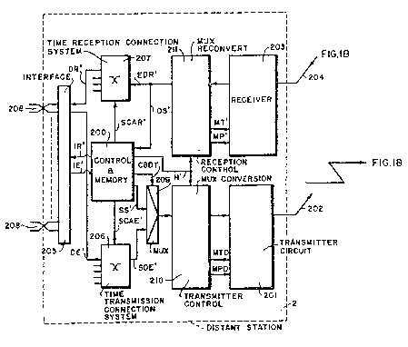
The structure of a distant station 2 is symme-
trical with that of central station 1. Distant stati~n 2 is
also monitored b~ a control and memory device 200 synchro-
nous with that of the central station and has a trans-
mission circuit 201 and an aerial 202 and a reception cir-
cuit 203 and aerial 204. Transmission and reception cir-
cuits 201 and 203 have the same characteri~tics as thetransmission and reception circui-ts 101 and 103 in central
station 1 and are al.so powered from a power supply U (not
shown on the figure). An interface device 205 provides
the link between control and memory device 200 and the
subscribers' sets with regard to the signals concerning
the various communication channe].s, with signa~s to be
t~ransmitted I~' and recei.ved signals IR'. The interface
~evice is also linked to the subscribers' sets with a time
transmission connection system 206 for the data DE' to be
transmitted and a time reception connection system 207 for
the received data DR'. Interface device 205 is connected
to the subscribers' sets via telephone pairs 208. Control
and memory device 200 monitors the operations of time
transmission connection system 206 via address contro~
signals SCAE' and of time reception connection system 207
via address control signals SCAR'. Output SDE' of time
transmi.ssion connection system 206 is connec-ted to a multi-
plexer 209 which also receives command signals and infor-
PHF 85 536 -6- 16-4-1986
mation SS' from channels and a control signal CBDT from
~ontrol and memory device 200. Once multiplexe~, these sig-
nals are transmitted to transmitter clrcui-t 201. Receiver
203 transmits the si~nals received to time reception con-
5 nection system 207 (signals EDR') and to control and memorydevice ~OO (si~nals OS').
According to the invention, the information trans-
mission system between at least two stations for the
transmission of information from free and engaged channels,
l whel-e each station has at least oneradio transmi.ssi.on and
one radio reception circuit powered from a power supply
and means for detecting the free or engaged channels is
no~eworthy in that it has means working with means of
detection to provide a process for creating a time multiplex
f~rmed by an elementary ~ield of duration T, in which the
information ~rom the engaged channe].s is grouped side-by-
side in said elementary field and means for reducing the
~ower consumption of the transmission and reception circuits
from the detection of free channels and to provide a
~0 normal power supply for the transmission and rece~tion cir-
cuits from the detection of the engaged channels.
In fact, control and memory device 100 works
together with means 100' to set up a procedure for grouping
the engaged channels side-by-side in the multiplex field.
This procedure will be described with reference to figure
.
According to one feature of the invention, the
information transmission system in which the elementary
m~llti~lex fields carry i.nformation concerning the service
and data channels is noteworthy in that it also comprises
means for grouping the elementary multiplex fields n by n,
while the service and engaged'data channels are grouped n bv
n and side-by-side in the new field obtained.
It is therefore of advantage to inser-t, into
3s central station 1, between multiplexer 109 and transmission
circuit 101, a multiplex conversion and transmitter circuit
control device 110; likewise between reception circuit 103
and the time reception connection system 107 and control
P~F 85 536 -7- 1 6-~-1 9~36
and memory de~ice 107, is also inserted a multiplex recon-
version and reception circuit control device 111. The output
of multiplexer 109 is connected to the input of device
110, which also receives a clock pulse H produced by control
and memory device 100.
~ ccording to another feature of the invention,
the information transmission system in which each central
or distant station has at least one transmission and one
reception circuit is noteworthy in that it comprises means
~or partl~ or totally cutting o~f and powering the trans-
mission and reception crcuits. Additional power is thus
~aved. The switch-on and therefore the powering of a trans-
n~ission or reception circuit is effected partly three
channels before the end of the field for units 101 L and
103 L, which take longest to resume operation, whereas
units 101 C and 103 C, which re~ume more quickly, are
powered one channel or less before the end of the ~ield,
so that all the transmission or reception circuits are
powered. Thus the transmission or reception circuit is once
2n more ready to transmit information at the start of the new
field.
From the input signals (multiplex, clock H), device
110 transmits a partial and -total resumption signal MP and
~lT respectively with the intention of partly or fully power-
ing transmitter circuit 101, and also converts the elemen-
tary multiplex of duration T into an elongated multiplex
o~ duration nT. Signal MP is applied to a switch 101 A
which, when signal MP is active, connects power supply U to
units 101 L of transmission circuit 101. Signal MT is
applied to a switch 101 B which, when signal MT is active,
connects power supplu U to units 101 C. When signals ~lP
and MT are active, the elongated mu]tiplex at the input of
the transmission circuit is then transmitted by radio to
distant station 2.
Likewise, multiplex reconversion and reception
circuit control device 111 which also receives clock pulse
H produce~ partial starting signal MP'C applied to switch
103 A intended to power units 103 L via power supply u;
7~
PHF 85 536 --8 - 1 6--4--1 986
and total starting signal MT'C applied -to switch 103 B
intended to power units 103 C via power supply unit ~ and
reconverts the elongated multiplex of duration nT into an
elementary multiplex of duration T.
A multiplex conversion and ~ransmlssion circuit
control de~7ice 210 lclentical to device 110 in central
station 1 is also inserted into distant station 2 between
multiplexer 209 and transmission circuit 201. Likewise, a
multiplex reconversion and receiver control device 211
a is also inserted between reception circuit 203 and time
reception connection system 207 on the one hand and control
and memory device 200 on the other. The output of multi-
plexer 209 is connected to the input of device 210, which
also receives a clock p~lse H' produced by control and
memory device 200.
Device 210 produces a partial and total starting
signal MPD and MTD respectively to power transmitter circuit
201 partly or fully and converts the elementary multiplex
into an elongated multiplex. When signals MPD and MTD
~0 are active, the elongated multiplex is then transmitted by
radio to central station 1 (with signals MPD and MTD pro-
duced in the same way as MP and MT).
Likewise, multiplex reconversion and reception
circuit control device 211, which also receives clock pulse
2S H', produces partial start signal MP' and total start
signal MT' and reconverts the elongated multiplex into an
elementary one, with signals MP' and MT' produced in com-
pletely the same way as signals MP'C and MT'C.
Figure 2 shows a multiplex comprising engaged and
free channels. In this mu]tiplex supporting the description,
a field TR consists ~f 32 channels V1, V2, V3, V4, V5,
V6, ... V29, V30, V31. Some channels are engaged and are
given the reference n, e.g. V0, V1, V2, V4, etc., while
others are free and are given the reference L, e.g. V3,
3s V6, etc. Such a channel configuration in the field may
exist before the means of the invention are applied.
It would be best to give a brief description of a
field, using the example of the aforementioned multiplex,
7~
PH~ 85 536 ~9- 16-4-1986
for a better understanding of the invention, although this
~ield structure shall by no means be limitative.
The elementary field, i.e. before the grouping
of n fields, comprises three service channels, so that a
32-channel field has 29 data channels. The rhythm, the
field and multi-field locking words and -the semaphore
channel are carried in the service channels. The data
channels carry the communications data. When a data channel
is not en~aged t it carries the rhythm.
The information transmission system of the in-
~ention in which the service channels carry the rhythm
signal, the field and multi-field locking words and the
semaphore channel is noteworthy in that the rhythm signal
is transmitted at the very start of the multiplex field.
Another feature of the transmission system is
that the cla~nel status information ~free or engaged) and
the number of the last channel in use are transmit-ted in the
multiplex.
The service channe~s are invariably grouped at
the start of the field, so that the field structure thus
~efil~ed is:
- channel 0 which, in the invention, invariably carries the
rhythm.
The rhythm si~nal i~ produced by a clock at half
~5 bit freguency, so that, when very few channels are in use,
the distant station can be properly resynchronised before
the arrival of the first significant information.
-- Channel 1 which comprises the field locking word and the
numher o~ the last channel in use.
3~ - Channel 2 which comprises the multi-field locking word,
the channel status information channel by channel and the
semaphore channe'.
In the example, the fie~d contains 32 channels
numbere~ from VO to V31, and each channel has an octet, i.e.
8 bits available.
The multi-fie]d comprises 32 fields numbered ~rom
O to 31.
In channel 1, the field locking word is presen-t
P~F 85 536 -10- 16-4-1986
in every other field e.g. in the even-numbered fields.
Li.kewise the number of the last channel in use is present
in every other field in the odd-numbered ones.
Channel 2 is divided between different lines:
- the semaphore line during the odd-numbered fields;
- the multi-field locking word during field O;
- the signals channe~. by channel during the even-numbered
fields from 3 to 30. The signals of 2 channels are
transmitted i.n an octet:
' aO bO cO dO a1 b1 c1 d1.
There are 4 signalling bits per channel.
Bits aO bO cO and dO represent the signal of
the channel with t~le same number of the field and bits a1
b1 c1 and d1 represent the signal of the channe] with the
same number as the fi.eld plus one.
sits a b and c represent the signal of the junc-
tion unit or the equipment to which the channel has been
allocated with bit d representing the status of the channel.
Channe~s 3 to 31 are allocated to the subscribers.
~O The multiplex configuration is thus:
PHF 85 536 ~ 16~4-1986
\ Ch.No. _ _
ield ~ VO V1 v2 V3 to V31
0 rhythm F`ield Multi- Voice
lock (VT) fie]d channels
lock (VMT)
1 rhythm Last ch. Semaphore "
No. (LCN) ch. (CS)
_ .
2 rhythm VT
_ rhythm LCN CS
_ __ rhythm _ __ _ S gnal
lS rhythm ICN CS ..
27 rhythm LCN CS
28 rhythm VT S i~n al ..
ch. 28t29
. . ._ .__
29 rhythm LCN CS
.
rhythm VT Si~nal
_ _ ch. 30+31
~5 31 rhythm LCN CS ..
__ rhythm VT VMT
The field lock octet is selected so that there
30 can be no imitation by the octet containing the number of
the last channel used. There is no problem here since only
5 bits are needed to transmit this number, giving the
following example of a configuration:
field lock octet 1001101_1
3 last channel No. octet 111 NDV
NDV = number of the last channel used.
Figure 3 shows the conversion of an elementary
into an elongated field. In the example described, 8 fields
7~
PHF 85 536 -12- 16-4-1986
have been grouped according to the invention.
The referenced channels of each elemen~ary field
number 3~: V0, V1, v2, V3, V4, ... V30, V31. The elementary
fields are grouped by n = 8: TRO, TR1, TR2, ... TR7, to
constitute an elonaged field T~A. Once the n = 8 elementary
fields have been grouped to form an elonga-ted field, the
channels V of the elementary multiplex are assembled side-
by-side in groups of ~ channels: 8VO, 8VI, ... 8V31. The
channels of the elongated multiplex are referenced M, thus
channel MO contains 8 elementary channels VO, channel M1
contains 8 elementary channels V1, ... and channel M31
contains 8 elementary channels V31.
Figure 4 puts forward a diagram of :central
station 1. Control and memory device 100 is monitored by a
control unit 1100 arranged around a micro-processor. It is
fitted with an address line BUSA and a data line BUSD and
is thus associated wi~h read/write memories (RAM) 1101, re~d-
only memories (ROM) 1102 and an interface box 1103 for
the running of the semaphore channel facilitating dialogue
hetween the central and distant stations. Interface device
105 consis-ts of junctions 1104a, 1104b, etc., providing
the link between central station 1 and the automatic se
lector in the telephone exchange (not shown) using tele-
phone pairs 108. There are as many junctions as there are
subscribers' lines to be connected. Control and memory device
l00 has a transmission time base l105 which provides con-
trol signals CBTE for the various junctions 1104a, 1104b,
etc. for the purposes of coding and decoding the l.f. voice
signals, recovering the transmitted signals (loop statuses)
and issuing orders (bells, rating, battery reversal) which
are detected on the link lines to the telephone exchange.
Control signal CBTE also controls time transmission con-
nection system 106. Device 100 also has a reception time
base 1106.
The voice channels are concentrated on the multi-
plex link lines after the detection of the li~ting of hit
set by a subscriber at a distant station, the data's being
transmitted by the semaphore channe], or information on a
7~
PHF 85 536 -13- 16-~-1986
new call generated by the automatlc selector in the tele-
phone exchange (not shown). The new call is detected by
device 100 via an order memory 1107 preceded by a multiplexer
110~ into which all the orders from the subscribers' junc-
tions, signal IE, are invariably written. Control unit 1100periodically reads this order memory 1107 via a multiplexer
1109 and thus detects changes in status.
A channel is allocated to a junction by time con-
nection system 106 and a command memory 1110 preceded by
multiplexer l 111 . The command memory 1110 of connection
system 106 and multiplexer 11 1 1 are located in device 100.
Connection system 106 essentially consists of memories
into which the coded l.f. channels from the junctions,
signals ~E, are systematically written. At the output of
connection system 106 there is now only one 32-channel link,
a signal SDE, if the selected multiplex has 32 channels.
Concentration is brought about by reading, in the time set
aside (signal CBTE produced by time base 1105) for the
output channel, the content of the word corresponding to
~0 the input channel which is to be used. The read-out addresses
are provided by command memory 1110, signals SCAE. To pro-
vide a channel, control unit 1100 thus writes the number
of the input channel which it wishes to connect into memory
1110 at the address corresponding to the output channel~
~5 Read-out addresses SCAE supplied by memory 1110 also serve
to write into command memory 1107 the signals to the channe]s
which have been concentrated (channel-by-channel signalling).
Correlatively, control unit 1100 writes the
occupational status of the channels into a 32 x 1 bit
channel occupation memory 1112, with which is associated a
multiplexer 1113. This memory is read at the same time as
command memory 1107, in this manner, channel-by-channel
signalling transmits the status of the channel, free or
engaged, at the same time as the signal of the junction which
has been connected. Read-in and write-out of command memorles
1107, control memory 1110 and channe] occupation memory
1112 take place in synchronism with transmission time base
1105, signal CBTS.
7~
PHF ~5 536 -14- 16-~-1986
Mult,iplexer 109 makes i-t possible to collect
on the multiplex link the voice channels, output signals
~DE of connection system 106 and the commands and signals
irom channels OS, which are:
s - Channel-~y-channel signalling SVV transmi.tted by command
1107 and channe] occupa~ion 1112 memories which, together
with c~ntrol unit 1100, constitute the means of detecting
free ~r engaged channels.
- The semaphore channel transmitted by interface box 1103.
- The number of the last channel used NDV, provided by con-
trol unit 1100 via circuit 1114 in which the number of
the last channel used is entered.
- The lock words of the field VT, and multi-~ieid MVT
and rhythm signal R, all produced by transmission time
base 1105 ~the field and multi-field lock words provide
recognition of the vari.ous channels).
Multiplexer 109 is controlled by control signal
C produced by transmission time base 1105.
The signal at the output of multiplexer 109 is
2d transmitted to transmitter circuit 101.
Reception circuit 103 transmits the information
received to time reception connection system 107, signal
EDR, and to device 100, signals SS. Signals SS comprise
the channel signals transmitted to a signalling memory 1115
in device 100 and the lnformation from the semaphore channe]
which is transmitted to interface hox 1103. The information
received also makes it possible to reconstitute reception
time base 1106 from the field lock words contained in said
information. This time base 1106 makes it possible to ex-
tract the various channels from the fie~.d and multi-field.
In de~7ice 100, signalling memory 1115 is pre-
ceded by multiplexers 1116 and 1117, whereas a command
memory 1118, preceded hy a multiplexer 1119, addresses
time reception connection system 107 via address command
signals SCAR.
Time reception connection system 107 and signalling
memory l l 15 operate in exactly the same way as time trans-
mission connection system 106 and command memory 1107 on the
5878
PHF 85 536 -15- 16-4-1986
transmission si.de. There is a single multiplex link, signal
EDR, at the input of connection system 107, whereas the
informat~.on received on a number of multiplex links, signals
DR, is transmitted at its output. Control unit 1100 writes
into com~and memory 1118 at the address corresponding to
an input channel of connection system 107 the number of the
output channels which it wishes to connect, defined at
the time by control signal CBTR produced by reception time
base 1106. Likewise the channel-by-channel signals con-
tained in the field are invariably written into signallingmemory 1115 at addresses SCAR provided by command memory
1118. Thus reading out of command memory 1118 and thus the
systematic write-in into connection system 107 and signalling
memory 1115 take place in synchronism with reception time
base 1106, signal CBTR, while the systematic read-out from
signalling memory 1115 and connection system 107 take place
in synchronism with transmission time base 1105, signal
CBTS.
Control unit 1100 writes the stand-by code i.nto
the addresses corresponding to the junctions which are not
connected to the input channels into signalling memory 1115.
The connection is the same in the transmission and reception
directions, the same channel is allocated to the same junc-
tion, signal IR.
According to one feature of the invention, con-
trol and memory device 100 works together with means 100'
to bring about a procedure for grouping the engaged channels
side-by-side in the multiplex field. In a preferred embodi-
ment of the invention, means 100' are ROM into which are
written the various statuses relating to the procedure
(described with reference to figure 6) used to group the
engaged channels side-by-side. Means 100' work together with
the means of detecting free and engaged channels consti-
tuted by control unit 1100, command 1107 and channel occu-
pation 1112 memories to set up said procedure. In parti-
cular, the microprocessor of control unit 1100 in relation
with means 100' via address line BUSA and data line BUSD.
In another feature of the invention, into central
PHF 85 536 -16- 16-4-1986
station 1, between multiplexer 109 and transmitter circuit
101, is inserted the device for converting the rnultiplex
and controlling the transmitter circuit 110; likewise, the
device for reconverting the multiplex and controlling the
reception circuit 111 is inserted between reception circuit
103 and time reception connec-tion system 107 on the one
hand and control and memory device 100 on the other. A
clock ~, generated by transmission time base 1105, is used
by devices 110 and 111. Device 110 transmits signals MT and
l~lP to transmitter circuit 101, while device 111 transmits
si~nals ~IT'C and MP'C to receiver circuit 103. Devices 110
~nd 111 t~ill respectively be described with reference to
fi~ures 7, ~ and 9,10.
Figure 5 puts forward a diagram of distant station
2, the structure of which is symmetrical with that of cen-
tral station 1. Control and memory device 200 is monitored
by a control unit 2100 arranged around a microprocessor.
Control unit 2100 has an address line BUSA' and a data line
BUSD' and is thus associated with R~M 2101, ROM 2102 and an
inter~ace box 2103 to run the semaphore channe]. Interface
device 205 provides the link between the distant station
and the suhscribers' sets via telephone pairs 208. It con-
sists of junction circuits 2104a, 2104b, etc. There are as
many junction circuits as subscribers' lines. Control and
~5 memory device 2100 has a single time base 2105, reconstitut.ed
from the multiplex received, which provides control signals
CBDT to the various junction circui-ts 210~a, 2104b, etc.
Likewise, the distant statlon has, on the reception side,
a command memory 2106 preceded by multiplexers 2107 and
~o ~108. All the commands (output signal IR') concerning the
subscribers' ju.nction circuits from the multiplex field
received (si~nals Os~) and the data supplied by control
unit 2100 in synchronism with signal CBDT provided by
time base 2105 are systema.tically written i.nto memory 2106
at the addresses su~plied by control unit 2100. The occupied
channel signal is also reinjected to the transmission
side vla multiplexer 209. A channel is allocated to a
junction circuit via time reception connection system 207
~ ti~ 3
PH~ 85 536 -17- 16-4-1986
~snd a command memory 2109 preceded by multiplexer 2110.
ilemcry 2109 and mu~.tiplexer 2110 are located in device 200.
At the input of time reception connection system 207 is
5 transmitted received multiplex ED~ while at its output a
number of multlplex links DR ' is transmitted to the various
junction circuits. Write addresses SCAR are provided by
command memory 2109. In order to allocate a channel
control unit 2100 writes the number of the input channel
lO which it wishes to connect into memory 2109 at the address
col-respol1ding to t.he output channel in synchronism with
siqnal CBDT produced by time base 2105. Write addresses
SCAR supplied by memory 2109 also serve to write the
cll~nllel signals into command memory 2106.
The data to be transmitted DE from the various
junction circuits are sent to the inputs of tlme trans-
mission connection system 206 at the output of which signal
SDE is transmitted on a single multiplex link to multi-
plexer 209. Command memory 2111 preceded by multiplexer
20 112 is writter at the ~ddresses defined by control unit
2100 in synchronism with signal CBDT provided by time base
2105. .;~lemory 2111 addresses connection system 206 by
means of address command signals SCAE . Likewise; signals
IE from the junction circuits are transmitted to signa~.ling
2~ memory 2113 assGciated with multiplexers 2114 and 2115. The
channel-by-channel signals are wri.tten into signalling memory
2113 in synchronism with signal CBDT of time base 2105.
~lemory 2113 is read by control unit 2100 at the addresses
de~ined by control unit 2100 to detect the lifting of hand-
30 sets. Memory 2l13 is also read from addresses SCAE pro-
vided by command memory 2111 and signals SIE are then
transmitted to multiplexer 209 which is controlled by
signal CBDT and co]lects the voice channels signals SDE
and the various signals SS on the multiplex link the
3~ latter being broken down thus:
- Channel-by-channel signalling SvV resulting from signals
SIE and the occupation signals of the channels.
- Semaphore channel CS transmitted by interface box 2103
.
PHF 85 536 -18- 16-4-19~6
which recei.ves the information (signals OS') from -the
multiplex field issued hy the central station.
- The lock words for the field VT and multi-field VMT and
rhyt.hm signal R from reconstituted time base 2105.
5 - The number of the last line used NDV from circuit 2116.
The number of the last line used is extracted from the
multiplex field issued by the central station, written
into circuit 2116 and retransmitted to multiplexer 209
in synchronism with time base 2105.
According to another feature of the invention,
into distant station 2, between multiplexer 209 and trans-
mitter circuit 201, is inserted multiplex conversion and
transmitter circuit control device 210. Likewise, between
reception circuit 203 and time reception connection system
~07 on the one hand and control and memory devi,ce 200 on the
other is inserted multiplex reconversion and reception
circuit control device 211. A clock H' emitted by recon-
stituted time base 2105 is used by devices 210 and 211.
Devices 210 and 211 are identical to devices 110 and 111
respectively in the central station. Device 210 emits
signals l~ITD and MPD to transmitter circuit 201, while de-
vice 211 transmits signals MT' and MP' to reception cir-
cuit 203.
With the description of the distant station com-
pleted, it should be noted that a few differences appear
~eyond the eY~isting symmetry between the central and dis-
tant stations. The distant station is in fact synchronous
with the central one, so that time base 2105 recovered on
reception is unique and thus also used on transmission.
3~ The contro]. of time connection systems 206 and 207 is also
specified by the central station. The number of the last
channel used written into cir.cuit 2116 whichis retransmitted
in the transmitted fie],d is taken from the received field.
~he occupation of the channels, retransmitted in channel-by-
channel signalling, is the same as that received in the in-
cident transmission, and is therefore a copy of the channel
signalling written into command memory 2106.
Figure 6 proposes a diagram of the appllcation
PHF 85 536 -19- 16-~-1986
of a procedure created to group the channels engaged in
the multiplex in a given configuration, in accordance wi-th
the invention.
The channels are allocated on the multiplex by the
central station on the detec~tion of an incoming call from
the te7ephone exchange or wheli a subscribel- connected to
a distance station lifts his handset.
In the example of an application below, and to
aid understanding, channe]s VO to Vi of the multiplex
are service channels (rhythm, field and multi-field synchro-
nisation and signalling) and are always present in the
fields. Channels Vi + 1 to Vn of the multiplex are data
channels varying between "free" and "engaged". A data
channel is regardec7 as engaged when a communication has
been associatecl with it. All -the da-ta channels are "free"
when the network is commissioned.
The service channels are always allocated at
the start of the field and, in order to make best use of
the Eield, the central station allocates the data channels
to the lowest priority from Vi -~ 1 to Vn on establishing
com~unications.
There are two possible cases for taking account
of calls: the call comes either from the telephone exchange,
or from a subscriber connected to a distant station (at
the moment when the subscriber lifts his ha~dset). The
procedure for allocating a channel is the same in both
cases and the diagram of figure 6 provides a system for
both. The procedure to be descrihed is created in device
100 via the means for detecting free or engaged channels
and by means 100' containing the various statuses of said
procedure.
In the first casedescribed, -the call is trans-
mitted by the tele~hone exchange. In the initial state POr
the associated junction is OJl stand~by. The incoming call
from the telephone exchange then sets up status P1, when
a channel allocation procedure must be followed so that,
according to the invention, the data channe:Ls ma~ be qrouped
side-by-side, for instance at the start of the field, with
~5~
P~F 85 536 -20- 16-4-1986
the service channels automatically allocated to the first
ti1ree. In the field channel application procedure, r, i and
n represent the rank of a c}~anne], i + 1 is the first rank
which can be allocated to a data channe1, n is the last, and
5 r the one specified at the time of allocation. The first
possible rank after i is r = i ~ 1, when s-tatus P2 arises.
A question arises immediately afterwards in status P3: is
channel Vr of rank r free? If not, one unit is added to
rank r and rank r ~ 1 is tested. This gives rise to status
P~. A further question of rank then arises in status P5.
Is the tested rank higher than n (the last possible one)?
If so, allocation is refused, status P6. All channels are
en~a~ed and the caller must repeat the call. If not, how-
e~rerl i.e. if the tested rank is lower than n, the system
returns to status P3: is the channel of the new rank
tested free? If it is engaged, the procedureis repeated
via statuses P4 and P5 as long as no free channel is found
or while allocation is not refused (state P6). When the
rested rank is free, status P7 arises, the tested channel
~o is declared en~aged (transmission of an engaged bit for
the channel~ and allocation is accepted: the junction is
put through. At the end of the communication, the channel
used is freed: this is status P8, the channel is declared
free (transmission of the channel engaged bit). The ]ast
~5 status P9 is equivalent to status PO, i.e. the junction
is again on stand-by.
The procedure for the second case is fully iden-
tical. In the initial state PO the subscriber's set is on
stand-by and status Pi is produced when he picks up his
handset. Statuses P2, P3, P4, P5, P6,P7 and P8 are those
described for the first case. Status P9 is also equivalent
to the initial status PO, i.e. the subscriber's set is once
more on stand-by.
In this method of operation, it is possible that
few channels are in used but the last channel used is at
the end of the field. The central station control unit knows
the occupation of the channels and their alloc~tion to the
subscribers. If this configuration lasts too long, the
~ 7 ~
PHF ~5 536 -21- 16-~-19~6
control unit realloc~tes t~le channels so as to collect the
engaged channels at the start of the field.
Thus, if traffic is heavy of calls take a long
time, certain high-ranking communications channels may
5 be engaged while a large number of lower-ranking ones have
become free. The central station decides to reorganise the
field in order to group the communications on low-rankinq
da.a channels.
This process consists in taking the communications
associated with hiqh ranking channels and replacing them
on free low-ral1king channels, depending on a set of para-
meters linked to the system channel concerned, viz:
N: number of current communications;
Vh: highest-ranking engaged channel;
h: rank of channel Vh;
D: average duration of a communication during the
past hour (expressed in hundredths of an hour);
C: number of communications established during
the past hour.
The organisation of the field is analysed at the
end of a time D. Its reorganisation is decided only if the
condition below applies:
(h x Di) N - x (x is selected by the operator).
This condition expresses the ratio between the
number of communications which may be establishe~ during
the period D to come and the number of free communications
channels between Vi and Vh. While this ratio is 1 or more,
it is not expedient to dictate a reorganisation of the
multiplex. If, however, it becomes much lower than 1, re-
organisation is imperative.
If reorganisation conditions exist, the central
station software transfers the communications associated
with the highest-ranking channels to the free lower-ranking
ones, beginning with the communication associated with the
highest-ranking engaged channel Vh~
Figure 7 proposes a diagram of the multiplex
conversion and transmitter circuit control device 110, which
PHF 85 536 -22- 16-4-1986
is identical to device 210.
The transmission system is noteworthy in that it
has means for reducing the power consumption of the trans-
mitter and reception circuit and power them normally on
the detection of engaged channels. The means for detecting
free or engaged chann~ls w~re described in the description
of the central station with reference to figure 4. This
consistsof control unit 1100 and command and channel occu-
pation memories 1107 and 1112 respectively.
As stated in the preamble, however, the response
time to the start-up of the transmission and reception
circuits is not negligible compared with the duration of a
multiplex field used generally ~or this type of equipment
te-g- the recurrence of a 32-channe] mu]tiplex is 125/us).
In order, therefore, to reduce the effect of their response
time and thus to increase the power saving with advantage,
the multiplex field is otherwlse organised.
To this end, the transmission system comprises
means for grouping the elementary multiplex fields n by n
and side-by-side in the new fields thus obtained. The (e.g.
3~-channel) elementary multiplex field is converted into a
field n times longer and the n channels of the same rank
are grouped side-by-side. There is a set of counters con-
sisting of a bit counter 1168, a channel counter 1170, a
~5 field counter 1171, and a memory selector 1172 facilitating
the addressing of a part of a memory. These four counters
are synchronous with the clock pulse H issued by time
base 1105 (figure 4) and in phase in relation to the field
tthey may form part of time base (1105). Multiplexer 109
~o controlled by signal C from time base 1105 (figure 4) makes
it possible to insert various signals in the elementary
field (before the fields are grouped n by n), e.g. rhythm
signal R, lock ~ords for the field VT and the multi-field
VMT, the number of the last channe] used NDV, channel status
si~nals SVV, semaphore channel CS and the signals relating
to the data channels SDE. The output of multiplexer 109 is
connected to the input of a serles-parallel converter 1174,
the output of which is connected to a memory circuit 1175.
587~
PHF 85 536 -23- 16-4-1986
The elementary multiplex is converted into an elongated
one by memory 1175 which may contain twice n fields. Half
of the memory contains the n fields of the elementary mul-
tiplex in the order of their arrival, while during this
write-in time, the other half of the memory is read out
in a different order to constitute the elongated multiplex.
Memory 1175 is monitored by the various address signals
from counters 1170 and 1171 and selector 1172, facilitating
a choice of the half of the memory concerned, while all the
signals are multiplexed by multiplexer 1176. The access time
to memory 1175 at the rate of the channe]s V is divided into
two: one for write-in and one for read-out. Multiplexer
1176 is controlled from a decoding circuit 1169 controlled
from the signals of bit counter 1168.
An operative example in which the selected figure,
n = 8, is not limitative, is proposed here to explain the
process.
Channel counter 1170 provides address wires Ao,
A1, A2, A3 and A4 by means of which the channels of the
initial elementary multiplex can be traced, while field
counter 1171 provides address wires A5, A6 and A7 by means
of which the n = 8 fields to constitute the elongated mul-
tiplex may be traced. "memory selector" 1172 provides
address wire A8 indicating the part of the memory concerned.
Writing into the memory is done into the half
indicated by the status of A8 at the addresses dictated by
commands A0, A1, A2, A3, A4, A5, A6 and A7.
The memory is read out in the half indicated by
the status of A8 at the addresses dictated by commands A3,
30 A4, A5, A7, AO, A1 and A2.
Writing into the memory is thus done in the order
for an ele~entary 32-channe] multiplex after it has been
decided to elongate it 8 times:
0, 1, 2, 3, 4, 5, 6, 7, 8, 9, ..., 253, 254, 255,
whilst read-out ta~es place in the order:
0, 32, 64, 96, 128, 160, 192, 224, 1, 33, 65, ....
225, ..., 255.
The output of memory 1175 is then connected to a
PHF 85 536 ~24- 16-~-1986
parallel-series converter 1177, the O~ltput of which is
connected to transmission clrcuit 101.
On transmission, then, the conventional elemen-
tary field is elongated and the transmission commands are
then drawn up. On reception, it will be shown with referen-
ce to figure 9 how the receiver commands are drawn up from
the elongated field received and how this elongated field
is reconverted into a conventional elementary fteld.
According to one of -the features of the trans-
mission system, channe~ status information (free or engaged)and the number of the last channe] used, on transmission
are us~d to draw ~p the signals to cut off and power the
tra~smission and reception circuits partly or fully.
The information transmission system is also
lS noteworthy in that, then the transmission of the channel
status information is used to cut off and power the trans-
mission and reception circuits partly or wholly, the
emission of a data channel after several free channe]s is
immediately preceded by the emission of a rhythm channe].
At present each channel lasts for the time of
n elementary channels and the channel validation informa-
tion is used to switch on and off units 101L (signal MP)
and lOlC (signal MT) of transmission circuit 101 instead
of basing switch-off solely on the rank of the last channel
used.
The partial start command for the transm-ssion
circuit is drawn up from a counter 1178 and a comparator
1179 which continuously compared the state of this counter
with the number of the last channel used NDV. SignalNDV
is taken at the input of multiplexer 109, and is -thus al-
ways present at the input of comparator 1179. The emission
frequency of the information on the channels from channel
counter 1170 is the clock which is applied to one input of
an AND circuit 1180, to the other input of which is applied
the inverted output signal of comparator 1179, so that the
output signal of circuit 1180 makes it possible to advance
the counter at the clock rate. As soon as the number of the
last channel used is equal to the state of counter 1178, the
ô ~
Pl3F ~5 536 -25- 16-4-1986
latter is stopped. The si~nal from fleld counter 1171 de-
coded by decoder 1181 makes it possi~le to ~ero counter
1178 (signal RZ) after detection of the last channel of the
field. The output of comparator 1179 is applied to the input
of a flip-flop 11~2, the second input of which receives
the clock p-1lse emitted at the transmission freyuency of the
information o~ the channels. Thus the output of flip-flop
1182 controls the partial start-up of the tra~smission cir-
cuit. The output of flip-flop 1182 is connected to an input
of an OR circuit 1183, a time is imposed on the second
in~ut of OR circuit 1183 obtained by decoding the time base
signals ~decoder 1181) and lasts for the last three channels
o~ t~1e ~ield. The signal at the output of circuit 1183 thus
el~sures a partial start three channels before the start of
the field (signal MP).
Full starting is provided from 32 x 1 bit memory
118~ containing the channel occupation. Writing into this
memory is carried out by a micro-processor (signal MPE)
which may be that of control unit 100 (here, all that is
needed is to connect and use data line BUSD). It is read
under the control of addresses CA (uslng the above example:
A3, A4, A5, A6, A7). The memory access time is divided into
two: a part for write-in and one for read-out. Writing-in
is performed by the microprocessor only when it is to change
the content of the memory (allocation or cancellation of
a channel). To this end, the micro-processor supplies, at
its address bus MPA (or BUSA, which is all that need be
conl1ected if control unit 100 is used), the address in which
it wishes to write and, on its data bus I~PE, the new infor-
mation to be written in. This separation between the write-
in and read-out times is brought about by means of a multi-
plexer 1186, at the input of which are the read-out and
write-in addresses. The command to this multiplexer comes
from a decoding circuit 1173, the inputs of which come from
counters 1168, 1170 and 1171. The memory is systematically
read on the command of addresses CA at the output of coun-
ters 1170 and 1171 two channels ahead. Addresses CA, con-
trolling the read-out from memory 1184, presented to the
PHF 85 536 26- 16-4-1986
input of adder circuit 1185, are provided by adder circuit
1185 two stages ahead, as the circuit automatically staggers
addresses CA by 2 steps. The output of circuit 1185 is con-
nected to one input of mul-tiplexer 1186, the second of
which receives the microprocessor address signal (signal
PA, or address line BUSA), with the out.put of the multi-
plexer connected to memory 1184. The output of the memoryis
connected to the input of a shift register 1187. The result
of read-out is memorised t.hree times in order to control
start-up two channels ahead of the actually engaged channel
and thus to make it possible to emit. a rhythm channel before
saicl channel. Three of the inputsof an OR circuit. 1188 are
connected to the three outputs of register 1l87 representing
the read-out from the memory plus the two previous read-outs.
lS A fourth input of this OR circuit 1188 receives a time
command from decoding circuit 1181. The length of this time
corresponds to the last channel of the field (i.e. the
channel preceding the new field) and to the three service
channels MO, M1 and M2. The output of OR circuit 1188 is con-
2~ nected to the input of an AND ci.rcuit 1189 which contro].sf~lll start-up (signal MT) of transmission circuit 101 wher.
its second input sees the active partial start-up signal
(~lP) thus val.idating full start-up.
The dealy of 20/us in relation to the control of
units 101C is taken by way of example, If this control acts
solely on the output amplifiers, the response time is neg-
ligible. Here, total start-up command ~IT should arrive at
the actual time of transmission. On the diagram of figure
7, it is necessary merely to read out memory 1184 with a
3n slight advance. Circuit 1185 then shifts addresses CA by
one step and shift register 1187 comprises only two stages:
the result of the read-out from memory 1184 is memorised
twice. The two OUtptlts of register 1187 are connected to
two inputs of OR circuit 1188. The time from circuit 1181
and forwarded to the third input of OR circuit 1188 corres-
ponds only to the three service channels MO, M1 and M2. In
these conditions, transm.ission thus be~ins at the start of
the field ~channel MO) and, if several channels are free,
PHF 85 536 -27- 16-4-1986
it begins one channel before the first engaged channel fol-
lowing, thus making it posslble to -transmit the rhyth~ se-
quence during this channel.
According to another fe~ture of the invention, the
5 transmission system is noteworthy in that the transmiSSiOn
of the number of the last channel used is used alone to
draw up the signals to cut of and power the transmission
and reception circuits partially or wholly.
It is in fact possible, if desired, not to use the
individual engaged channel information and draw up commands
for de~rlce 101 solely from the information on the number
o~ the last channel used NDV. Here, complete start-up is
no lon~er commanded from the content of memory 118~ but
~rom the info~mation supplied by the output of flip-flop 1182
(see flgure ~!. If the response time of circuit 101C is
equivalent to the duration of a channel, -this signal is taken
to the input of an OR circuit 1183' and a time is imposed
on the second input of OR circuit 1183'. This time is sup-
plied b~ decoding circuit 1181 from the signals from coun-
ters 1170 and 1171 and corresponds to the last channel ofthe field. Control signal MT is then at the output of cir-
Cuit 1183'. If circuit 101C consists only of amplifiers,
its response time is negligible, when control signal MT
is issued directly by flip-flop 1182: transmission starts
in channel MO and continues uninterruptedly until the last
engaged channe]. The device of figure 8 is identical to
that of ~igure 7 regarding the ~rawing up of the par-tial
start-up signal and the multiplex conversion. Only the
drawing up of the full start-up signal is different, for
which circuits 1173, 1184, 1185, 1186, 1187, 1188 and 1189
and address signals CA are omitted or not used, whi]e
ci.rcuit 1183' is added.
Figure 9 proposes a diagram of reception circuit
211, identical to device 111. On reception, de~ice 211 is
very similar to device 110 on the transmission side, but
the time base is no longer set up locally but is recon-
stituted from information existing in the incident multi-
plex. A field lock tracing system correctly positions the
PHF ~5 536 -2~- 16-~-1986
time base counters i.n rela~ion to the lock words existing
in the multiplex.
The elongatecl multiplex is reconverted into an
elementary one with the aid of a memory 2130 which can
contain two fields of the elongated multiplex. The infor-
mation (marked DA' in the figure) contained in the incident
multiplex and present at the output of reception circuit
203, and clock H' issued by control and memory device 200
and synchronous with the multiplex clock, are transmitted
to the input of device 211 where they are converted by series-
parallel converter 2131 before being written into memory
2130. The output information of the memory i5 then recon-
v~rted by a parallel-series converter 2132 for transmission
to time reception connection system 207 and control and
memory device ~00.
In order to reconstitute the elementary multiplex
comprising 32 channels V (as in a previous example), it is
necessary to reconstitute a~time base from the field lock
information contained in channel M1 (second channel of the
~ elongated multiplex). The first octet of channel M1 always
consists of the field lock word. The loss and recovery
criterion of the f:~eld lock may be selected, by way of
example, from among the following rules:
- loss criterion: lock is regarded as lost when the absence
of at least one field lock word from among the four in
channel M1 is detected three~ times in succession;
- response criterion: lock is regarded as recovered when
the alternate presence and absence of the field lock word
has been detected four times.
Fie]d lock detection device 2133, to the inputs
of which information DA' and clock H' are also transmitted,
is a conventional device which counts the number of absences
~f the lock word before deciding on the field lock loss,
then supplying a field lock loss signal PVT. From -then on,
it seeks the reason for locking on all incoming bits. As
soon as it finds a lock word it awaits the checking of its
presence and absence four times before deciding to resume
locking.
PHF 85 536 -29- 16-4-1986
The time base is then reconstituted by ~eans of a
series of synchronous counters of clock H', with the outpu-t
of frame lock detection device 2133 providing the information
needed to reconstitute the time base at the input of the
various counters. Counter 2134 advances at bit rate e1e-
mentary channel counter 2135, w~ich is an 8-counter giving
the elementary channels in a c~annel of the elongated mul-
tiplex (addresses AO, A1, A2), channel counter 2136 which
~ives the addresses of the elor,gated multiplex channels
o ~ddresses A3, A4, A5, A6, A7) and finally memory selector
2137 which provides address wire A8 to indicate (according
to the status of A8) the half of memory 2130 concerned. The
information at counters 2135, 2136 and flip flop 2137 is
transmitted to multiplexer 2138 which provides the addre~s
information for memory 2130, thus ensuring the reconversion
of the elongated into an elementary multiplex. The acces~
time to memory 2130 at the channel rate V is divided into
two: one for writing and one for reading. Command C' from
multiplexer 2138 making it possible to provide addresses to
the memory arises from a decoding circuit 2139 controlled
by the si~nals from bit counter 2134 and channel counter
2135.
Writing into the memory is carried out in the
half indicated by the status of A8 at the addresses dictated
2s by commands A0, A1, A2, A3, A4, A5, A6 and A7.
Reading out of the memory is carried out in the
half indicated by the status of A8 at the addresses dictated
by commands A5, A6, A7, A0, A1, A2, A3 and A4.
Writing into the memory thus takes place in the
order 0, 1, 2, 3, 4, 5, 6, 7, 8, 9, ..., 253, 254, 255,
whereas readout takes place in the order 0, 8, 16, 24,
32, ..., 248, 1, 9, 17, 25, ..., 247, 255.
The time base thus reconstituted makes it possib]e
to extract the number of the last track used, which is in
the odd-numbered oc-tets of channel M1. In order to prevent
transmission errors, two identical consecutive numbers must
be received in order to be considered. This function is
performed by means of two re~isters 2140 and 2141, in which
PHF 85 53G --30-- 1 6--4--1 9~6
the octets of the incoming multiplex are -tr~nsferred at
times AOA1 of channel Ml (signal T1 transmitted to regis-
ter 2140) and AOA1 from channel. M1 (si~nal T2 transmitt.ed
to re~ister 2141), which represent the octets of rank 4n -~1
and ~n + 3 of channe] M1 with n = O or 1. Signals Tl and T2
are obtained by decoder 2142 Erom coun-ter 2135. If the
contents of both registers 2140 and 2141 are equal, as dis-
covered by cQmparator 2143, this content is transferred into
a third register 2144 at -time AO (si.gnal T3 issued by coun-
ter 2135), validated by an AND ga-te 2145 which receives
the output signal from comparator 2143 at one input and
signal T3 at the other. The content of this third register
corre~ponding to the number of the last channel used is
sy~tematically compared by compar~tor circuit 2146 to the
status of a channe~ counter 2147 in order to control the
partial switch-on of units 203L of reception circuit 203.
O~eration is then identical to that of device 110 descrihed
for the transmission side. A clock signal from elementary
channel counter 2135, the frequency of which corresponds
to that of the information concerning channels M of the
elongated multiplex, is transmitted to one input of an AND
~ate 2148 and one of a flip-flop 2149. The output of com-
parator 2146 is applied on the one hand to the second input
of AND gate 2148 after inversion and on the other to the
second input of flip-flop 2149. The output signal of AND
circuit 2148 thus makes it possib~e to advance channel
counter 2147 at the clock signal rate, while the output
signal of flip-flop 2149 is the control signal to switch
reception circuit 203 part].y on. Infor~ation from elongated
multiple~ channel counter 2135 is decoded by decoder 2150
which zeroes counter 2147 after detection of the last channel
of the field and transmits a time generated by the time base
to an input of OR circuit 2151. This time corresponds to
the three channels preceding the start of the new field.
The control signal for the pa.rtial switch-on of the recep-
tion circuit from flip-flop 214g is sent to a second input
of OR circuit 2151. Thus the signal at the output of OR
circuit 2151 ensures partial switch on MP' three channe].s
PHF 85 536 -31- 16-4-1986
before the start of the field.
Full switch-on is provided Erom 32 x 1 bit memory
2152 containing the occupation status of the channels which
may ~e written in e-ther by a microprocessor (which may
be that of control unit 200) if the engagement of the
channels is transmitted by semaphore channel or systema-
tically from a mu~ti-field time base 2153 reconstituted
with the aid of the elementary multiplex (signal taken
from the output of parallel-series converter 2132) and com-
prising mu]ti-field counters. The output signal from
parallel-seriec converter 2132 is applied to one input of
a m~llti-field lock detection device 2154 with a configura-
tion similar to that of device 2133. The information at
counters 2135 and 2136 is also transmltted to device 2154.
I~ a multi-field lock loss is detected, device 2154 supplies
a multi-field lock loss signal PVM and seems the reason for
locking in the same way as device 2133; if, however, lock
is retained or restored by device 2154, the multi-field
time base is reconstituted and the information passing
through multiplexer 2155 is transmitted to memory 2152.
The access time to memory 2152 is divided into
two: a time set aside read out and one for write-in.
This memory is actually organised into 16 x 2 bits since
the state of occupation of two channels is found in channel
~72 of the even-numbered fields~ Writing into the memory is
performed during channel V2 of the even fields at the
addresses provided by multi-field counter 2153. The memory
is read under the control of addresses CA (A3, A~, A5, A6,
A7) at the output of counter 2136 of the elongated multiplex
two channels ahead. Addresses CA in fact controlling the
read-out of memory 2152 are supplied by adder circuit 2156
two stages in advance, while the output of circuit 2156 is
connected to one input of multiplexer 2155. The command
for the latter comes from a decoding circuit 2157 controlled
by signals from multi-field time ba~e 2153 and channel
counters 2135 and 2136. The two outputs of the memory are
connected to the inputs of a multiplexer 2158 controlled
by signal T4 and time A3 from counter2135 which makes it
P~l.F 85 536 -32- 16-4-1986
possible alterl1ately to select one or other of the outpu-ts.
The output of ml)ltiplexer 2158 is connected to the input
Of A shift circuit 2159 and memorised three times in order
to control the switch-on two channels ahead of the actually
5 engaged channel. An OR ci.rcuit 2160 with three inputs con-
nected to the three outputs of register 2159 represents the
memory read-out plus the two previous read-outs. The fourth
input of OR circuit 2160 receives a time from decoder cir-
cu-t 2150. This time corresponds to the channel preceding
l0 the newfield (last channel of the field) and its three
service channels MO, M1 and M2. The output of OR circuit
~160 is connected to the .input of an AND circuit 2161 which
controls the full switch-on (signal MT') of units 203C of
reception circuit 203 when its second input sees active
lS E)artia:l switch-on signal MP', this validating full switch-
on
Moreover, the information transmission system, which
also comprises, included in the device for reconverting
the multiplex and controlling the reception circuit, de-
20 vices for detecting the field and multi-field lock respec-
tively providing a frame lock loss and/or multi-frame lock
loss signal in detection of such losses, is noteworthy in
that it comprises in addition, included in the device for
reconverting the multiplex and controlling the reception
25 circuit, an alarm circuit supplyi.ng an alarm signal to
dictate the full powering of the reception circuit after
the detection of field and/or multi-field lock losses.
If, indeed, field or multi-field lock is lost,
an alarm signal is supplied via an alarm OR circuit 2162
to the inputs of which are transmitted signals PVT of
field lock loss and PVM multi-field lock loss, and the
output of which supplies alarm signal AL. When it exists,
the latter is sent to a third input of OR circuit 2151,
causing units 203L to be switched on and to one of the two
35 inputs of an OR circ-lit 2163 which, at i.ts second input,
receives the full switch-on signal, thus fully switching
on units 203C of the reception circuit, while the time
bases will not be completely blocked. These commands are
PHF 85 53~ -33- 16-~-19~6
necessary to ~ive the station full access to the entire
multiple~ on stating or in the event of a shift and thus
to reset its time ~ases. While, there~ore, the time bases
are not properly positioned and the various signals cannot
5 be correctly received, comman~s MP' and MT' are active.
If, instead of writing the channel occupation
information into memory 2152 from the signals in channel V2
of the even fields, the information is written by a micro-
processor through dialogue via the semaphore channel -- and
this microprocessor may be that of control unit 200 -- the
memory circuit is slightly altered. The memory is organised
in 3`~ ~ 1 bits, with the information to be written in
supplied viy data bus MPE' of the microprocessor, which
may be data line BUSD' of the MicrOprOcessOr of control
l~ unit 200. The write-in address in the memory comes from
address hus MPA ' of the microprocessor which may be address
line BUSA ' of control unit 200 and the read-in address is
always signal CA (A3, A4, A5, A6, A7) present at the output
of counter 2136 two channels ahead. There is no longex any
need for multiplexer 2158 at the memory output.
If desired, no use need be made of the individual
~hannel occupation information; the commands of device
~03 may be drawn up solely from the information on the
number of the last channel used NDV. Here, partial switch-
on is no longer controlled from the content of memor~
2152 but from the information provided by the output of
flip-flop 2149 (see figure 10). This signal is connected
to one input of an OR circuit 2151' and a time is dictated
at a second input thereof. This time is supplied by decoding
circuit 2150 from the signals from counter 2136. This time
corresponds to the last channel M of the field. This OR
circuit 2151' has a third input connected to the output
of OR circuit 2162 supplying alarm signal AL in the event
of the loss of the field and/or multi-field lock. The output
of OR circuit 2151' supplies the full switch-on signal
MT' which thus starts one channel ahead of the start of
the field and lasts until the last channel used e~cept in
the event of an alarm, when it remains as long as the time
PHF 85 536 -34- 16-~-1986
bases have not been properly positionecl. ~'he ~evice of
fiqure 10 is identical to that of figure 9 as regar~s
the drawlng up oE the partial switc~-on slgnal and the
recon~ersion of the multiplex. Only the drawing up of the
full switch-on signal differs, and to this end circuits
2152, 2153, 155, 2156, 2157, 2158, 2159, 2160, 2161,
2163 and control signals T4 and address signal CA are
omitted or not used, while clrcuit 2151' is added.
Figure 11 shows a variant of the transmission
ln system using more than two stations. The lnformation is
transmitted via Hertzian channels between central station
l attached to telephone exchange 6 via telephone pairs 108
and a number of distant stations 2, 3, 4, 5, etc. The
dista~t st~tions may be subscribers' terminals, e.g. 2, 3
and ~, connected to the subscribers via telephone pairs
20~3, 30~ and 408 respectively, and may also be repeater
stations like 5 to which subscribers may also be directly
linked. The central, repeater and terminal stations are
interconnected by radio, transmitting and receiving infor-
mation via transmission and reception circuits. The centralstation is fitted with transmitting circ-lit 101 and recep-
tion circuit 103,terminal stations 2, 3 and 4 are fitted
with transmission circuits 201, 301 and 401 and reception
circuits 203, 303 and 403 respectively, and in particular
2~ repeater station 5 is fitted with a transmission circuit
501 and a reception circuit 503 to transmit and receive
information to and from central station 1 and also has
a transmitter circuit 501' and a reception circuit 503' to
transmit and receive information to and from terminal
stations 2, 3l 4, etc.
For a transmission system with more than two
stations as described above, it is thenpreferable to use
the TDMA (Time Distrihuted Multiple Access) princlple
for transmissions from the distant to the central stations
so that all neighbouring stations like statlons 2, 3 and 4
may transmit on a single~ radio frequency. The delays of
the various stations are adjusted so that the information
arrives properly staggered in tlme at the repeater station(s)
'7~
P~F 85 536 -35- 16-'1-1986
(station 5! and from central station 1. The information con-
cern~ng one channel transmitted by a station is grouped
ln the form of a bunch with a waiting time, so that the
various bunches do not overlap at a repeater or the central
sta.ion. Such a procedure is described in the previously
cited publication "COMMUTATION ~ TRANSMISSION" No. 3,
September 19&l, under the title "Sys-tème de téléphone rural
IRT 1500". The previously described mul-tiplex organisa-tion
is, of course, retained, for the direction from the central
to the distant stations.
The information transmission ~ystem using -the
TD~ principle for the transmission direction from the
distant to the central stations is noteworthy in that it
uses means of allocating the information bunches side-by-
side in the field. In the transmission direction, in fact,the principle of the concentration of the allocated bunches
side-by-side at the start of the field is conserved in
order to facilitate the commands for activating the trans-
mission and reception circuits of the repeater station(s).
The means used are similar to 110, 211 respectively described
~ith reference to figures 7, 8, 9 and 10 after the operation
~E the procedure described with reference to figure 6.
In fact,the information from a channel is issued
in the form of a bunch which may, for example~ have the
following structure: several rhythm octets, one bunch
start octet, one channel signalling octet and data octets
~oncerning the channel involved. The bunches are separated
by a delay in order to prevent any overalp on reception.
There is a time base for the bunch f~eld. For transmission,
the position of this time base in relation to the time base
reconstituted from the multiplex received is adjusted so
that the bunches arrive with the proper spacing in the
stations, e.g. 5 or 1.
On transmission, the partial and full switch-on
control signals MP and MT are drawn up . Signal MP begins
beEore the start of the field and continues to the end of
the last bllnch used. The number of the last bunch used is
extracted from the multiplex received in the station. This
~ '7~
P~ 5 53~ -36 16-4-1986
si~nal ~IP is produced from a time supplied by the time
base of tlle ~unch f1eld and from the signal showing equality
between a time counter and -the number of the last bunch
used. Signal MT is supplied by a bunch occupation memory.
This memory is read at the bunch transmission rate. The
result of the read-out is memorised only once, as the start
of the bunch transmitted contains rhythm information.
On reception, the partial switch-on command
signals ~IP' and I~IT' are drawn up. Signal MP' begins before
the start of the field and lasts to the end of the last
buncl1 used. It is also produced from a time provided by the
time base of the bunch field and from the signal showing
equality between a time counter and the number of the last
bunch used. S~gnal MT' is supplied by a bunch occupa-tion
memory. This memory is read at the bunch rate. The read-
out is performed before the arrival of a bunch (about
20/usec) and then memoriced at the start of the bunch. An
OR circuit obtained from these two items of information
thus gives a signal which beginc 20/us before the start
of a bunch used and ends at the end of this bunch.
In accordance with the idea of the invention,
transmission circuits 101, 501' are preceded by a device
for converting the multiplex and controlling the trans-
mission circuit so that device 110 in station 1, reception
circuits 203, 303, 403 and 503 are followed by a device
for reconverting the multiplex and controlling the recep-
tion circuit so that device 211 of station 2, transmission
circuits 201, 301, 401 and 501 are preceded by means similar
to means 110, which, on the transmission side, have been
described above, with reception circuits 103 and 503' fol-
lo~ed by means similar to means 211 which, on the reception
side,have been described above.