Note: Descriptions are shown in the official language in which they were submitted.
`-- ~66~
--1--
POWER MEASURING APPARATUS
.
The present invention relates generally to power
measuring apparatus and deals more particularly with an
improved apparatus or circuit for producing an output
signal proportional to the product of two input signals.
Generally the power supplied to an electrical
device such as, for example, a home appliance, can be
determined from the resultant product of the magnitudes
of the voltage measured across the input terminals to the
device and the current supplied to the device. Power
measuring apparatus, such as power meters, power monitors
and the like are often designed to operate with and
compute power from voltage and current signals having
sinusoidal waveshapes and magnitudes within a
predetermined range. Power measuring apparatus of the
aforementioned type generally have a limited dynamic
measuring range and require sinusoidal waveshape signals
for proper operation. However, voltage and current
waveshapes are not always sinusoidal and may often exceed
anticipated maximum values. It is useful and desirable
i~ many instances to know the mean instantaneous power
supplied to a device and therefore the measuring
apparatus must be capable of operating with instantaneous
voltages and currents varying over several orders of
magnitude.
In order to more accurately measure power for
voltage and current magnitudes outside a preselected
~ ~ .
rangej a different power measuring range corresponding to
the magnitudes of the particular range of voltage and
current associated with the electrical device being
measured must be selected, which selection conditions the
measuring apparatus to operate in the selected measuring
range. For example, a power range selected in a
measuring apparatus having an accuracy of 1~ full scale
reading would read within + 20 watts of the actual power
reading when the 2,000 watt range is selected; that is, a
power of 2,000 watts might be indicated in the range of
1,980 to 2,020 watts and a power of 200 watts might be
indicated in the range of 180 to 220 watts. It is
readily seen that the 200 watt reading using the 2,000
watt selected range is subject to an approximate error of
10~. Therefore, it is necessary to select a lower
maximum measuring range, say 200 watts, to measure with
an accuracy of + 2 watts. It will be seen that a
measured power of 2 watts might not even be read when
measured with a 200 watt selected range. Consequently,
either the user or the power measuring apparatus itself
must select an appropriate measuring range to obtain a
reasonably accurate power measurement at a full scale
reading.
Changing the selected measuring range to
accommodate fluctuating input voltage and current signals
or varying operating conditions of the electrical device
connected to the measuring apparatus is often
inconvenient because the user may be making repairs,
--3--
adjustments and the like to the device while observing
changes in the measured power and the changes may cover
one or more ranges. Auto-ranging power measuring
apparatus is generally very costly and possesses accuracy
characteristics similar to manually range selected type
power measuring apparatus.
One problem often associated with the lack of
accuracy over a wide measuring range in a low cost power
measuring apparatus is the presence of a DC offset
voltage in the power output signal. The output signal is
generally produced by a multiplier circuit oE some type
which computes the product of the voltage and current
supplied to the electrical device connected to the
measuring apparatus.
The voltage-current product computation can be
implemented using a standard commercially available
four-quadrant analog multiplier integrated circuit
however, power measuring apparatus implemented using such
integrated circuits generally exhibit an output error due
to the presence of a DC offset voltage in the output
signal and which error is generally in the range of 1
of full scale for the measuring range selected. In
addition, integrated circuit multipliers are generally
costly and require several external components to
function properly. Other, more conventional, multiplier
circuits implemented using low cost, discrete components
also exhibit static output errors in the range of 1 ~ of
full scale due to DC offset voltage in the output signal
91C~
--4--
caused in part by circuit components having unmatched
characteristics and in part by the design of the
multiplier. The DC offset voltage can be reduced
somewhat by utilizing circuit compensating techniques
such as null suppression and balancing. Generally such
compensation also requires additional circuit components
and adds to the cost and complexity of the multiplier
circuit and the power measuring apparatus.
The purpose of the invention is therefore to
provide a low cost easily implemented multiplier circuit
for producing an output voltage signal proportional to
the product of two unknown input voltage signals
particularly useful in implementing a low cost power
measuring apparatus.
Another aim of the present invention is to
provide a digital readout power measuring apparatus
constructed using low cost, standard solid-state
components and having a wide dynamic measuring range in
the order of 200 to 1.
It is yet a further aim of the present invention
to provide a multiplier circuit for producing a DC output
voltage proportional to the product of two input voltage
signals which DC output voltage signal has substantially
zero DC offset voltage to produce a static output error
of substantially less than 0.05 ~ of the full scale
reading.
Other objects and advantages of the invention
will be apparent from the following description and
~;6~9~
claims taken in conjunction with the accompanying
drawings.
The invention resides in an apparatus for
measuring the mean instantaneous power supplied to an
electrical device by computing the product of a first and
second voltage signal each being proportional to the
instantaneous voltage and current respectively supplied
to the electrical device. The product is a third voltage
signal proportional to the mean instantaneous power
supplied to the device.
The invention more specifically resides in a
self-biasing current source circuit for generating a DC
current signal proportional to the magnitude of the
second voltage signal and a logarithmic-anti-logarithmic
(log-antilog) multiplier circuit coupled to the current
source and the first voltage signal to compute the
product of the first and second signals.
The invention also specifically resides in a
current mirror circuit which removes the DC offset
current components associated with the ouput signal
current computed by the log-antilog circuit and the
self-biasing current source circuit.
Fig. 1 shows a perspective view of a power meter
having circuitry embodying this invention.
Fig. 2 is a functional diagram part in schematic
form and part in block diagram form, of the power meter
of Fig. 1.
-~ ~26~9~
--6--
Fig. 3 is a schematic diagram of one embodiment
of the eircuitry of the present invention.
Referring now to the drawings and considering
Fig. 1 in particular, a power meter having a digital
display and embodying the present invention is shown
therein and is designated generally by the numeral 10.
The illustrated power meter 10 is arranged to be
electrically connected between a conventional AC
electrical outlet via a standard 110 volt AC plug 12 and
an electrical device whose power is being measured. The
device is electrically coupled to the power meter by a
conventional AC receptacle 14. The magnitude of the
voltage and current supplied to the electrical device
being measured is sensed by an electrical circuit within
the meter and designated generally at 16 to produce a
first voltage signal proportional to the magnitude of the
instantaneous voltage supplied to the electrical device
and a second voltage signal proportional to the
instantaneous current supplied. A multiplier circuit
embodying the present invention and also within the
circuit 16 computes the product of the sensed voltage and
current signals to produce an output signal represen-
tative of the mean instantaneous power supplied to the
eleetrical device. The output signal is conditioned by
other circuit means within the circuit 16 to drive a
four-digit seven segment display designated generally at
18 to show in numerical form the magnitude of the mean
.: ,., . . -
6~
instantaneous power supplied to the electrical device
connected to the meter.
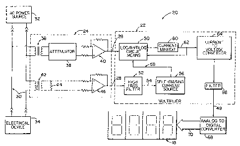
Referrinq now to Fig. 2 a block diagram
illustrating the major functional components of an
embodiment of the power meter of Fig. 1 is shown therein
and is generally designated by the numeral 20. A
multiplier circuit embodying the present invention is
included within the dashed lines and is generally
designated by the numeral 22. A sensing and scaling
circuit designated generally at 24 provides voltage
signals proportional to the sensed voltage and current
input signals to the multiplier 22 on leads 26 and 28
respectively. The power to be measured flows in a
circuit comprised, for example, by a pair of voltage
transmission line conductors 30. In one use of ~he power
meter embodying the present invention, the pair of
conductors 30 carry conventional and commercially
available AC electrical power from an AC power source 32
to an electrical device 34. A suitable voltage
transformer 36 designed to operate over the range of
approximately 50 to 600 volts AC is connected across the
conductors 30 to sense the voltage supplied to the
electrical device 34 and to couple the sensed voltage to
an attenuator 38. The attenuator 38 functions as a
voltage divider to reduce the sensed high voltages to
lower magnitude voltages for compatability with the
solid-state semi-conductor devices used in the apparatus
20. A differential input instrumentation amplifier
~ ~. \
~26~
--8--
circuit generally designated at 40 i9 connected to the
output of attenuator 38 and senses and amplifies a
voltage, when present across its input terminals, to
provide an amplified AC signal at its output connected to
lead 26 proportional to the instantaneous voltage
supplied to the electrical device 34.
A standarc3 current transformer 42 having a
primary and secondary winding has its primary winding
coupled to one of the pair of conductors 30 and the
transformer, in the illustrated example, is designed to
provide a current transformation from 2,000 amperes to 5
amperes. A resistor 44 is connected across the secondary
winding and senses the transformed current, when present,
to develop a voltage drop across its terminals propor-
tional to the current flowing through it. The resistor
44 is selected to provide a maximum voltage drop of 250
millivolts when a maximum 5 amperes transformed current
is supplied to the current transformer secondary winding.
A differential input instrumentation amplifier circuit
designated generally at 46 is coupled to the current
sensing resistor 44 and senses and amplifies a voltage,
when present across its input terminals, to provide an
amplified AC signal at its output connected to lead 28
proportional to the instantaneous current supplied to the
electrical device 34.
A high pass filter generally designated at 52
conditions the voltage signal appearing on lead 28 and
feeds the conditioned signal via lead 54 to the input of
-~ ~ 2~
a dynamic, self biasing current source generally
designated at 56 which current source forms an important
feature of the present invention and is explained in
greater detail hereinbelow. For present purposes it is
sufficient to say that the current supplied by the
current source 56 at its output on lead 58 varies in a
direct relationship with the magnitude of the input
voltage signal on lead 28 to maintain linear operation
over a wide range of input voltages and accommodates in
the illustrated embodiment an input voltage signal
corresponding to a current flowing in the transmission
conductors 30 ranging from 0 to 2,000 amperes
peaX-to-peak.
The current signal on lead 58 and the voltage
signal on lead 26 are multiplied together by a
log-antilog circuit means generally designated at 50.
The output of the log/antilog circuit is fed to the input
of a current mirror generally designated at 60. The
current mirror 60 produces a current signal at its output
on lead 62 which is fed back to the log-antilog circuit
50 to insure that the circuit 50 operates linearly and to
cancel DC currents produced by the multiplication
process.
The output current signal from the current
mirror 60 is also fed to a DC current-to-voltage
converter generally designated at 64. The output of the
voltage converter 64 is fed to a low pass filter 66 to
smooth out any ripple in the output voltage signal due to
~ 6609CI
' 10-
the multiplication process to produce a DC output voltage
signal on lead 48 proportional to the mean instananeous
power.
The DC signal on lead 48 is fed to an
analog-to-digital convertor generally designated at 68.
The convertor 68 senses the DC level present at its input
and converts the signal to a digitally formatted signal
representative of the DC voltage signal level present at
its input. The digitally formatted signal is applied to
a segment driver bus 70 in the proper signal format to
drive the four-digit display unit 18. The display unit
18 provides a numeric representation of the magnitude of
the mean instananeous power supplied to the electrical
device 34. The analog-to-digital convertor 68 may be
implemented by a commercially available integrated
circuit, such as, for example, a multi-digit direct
display drive analog-to-digital converter manufactured by
Teledyne Semiconductor.
Referring now to Fig. 3 and to the detailed
circuit schematic shown therein, a multiplier circuit
embodying the present invention and corresponding to the
multiplier circuit 22 of Fig. 2 operates as described
hereinbelow. As previously described, a first voltage
signal representative of the instantaneous voltage is
supplied to one input at lead 26 and a second voltage
signal representative of the instantaneous current is
supplied to a second input at lead 28. The first and
second voltage signals are multiplied by the circuit 22
to produce a third voltage signal product at the output
lead 48 proportional to the mean instantaneous power.
The input voltage signal at lead 26 is coupled
to the inverting input of an operational amplifier
generally designated at 72 to produce an inverted voltage
signal at its output 74 equal in magnitude and of
opposite phase ~o the input voltage signal at lead 26.
The non-inverting input to amplifier 72 is connected to
electrical ground potential via conductor 76. The input
signal appearing on lead 26 is also coupled through
resistor 78 to a first input logarithmic computing device
80 and the inverted input signal on lead 74 is coupled
through resistor 82 to a second input logarithmic
computing device 84.
The first and second input logarithmic computing
devices are formed by NPN transistors each having diode
connected base and collector terminals to provide a PN
junction. In accordance with the characteristics of a PN
junction, the voltage developed thereacross is
logarithmically related to the base e to the junction
current. The collector-emitter circuit of transistor 80
is connected to the base of NPN transistor 86 which
transistor 86 forms a first output anti-logarithmic
computing device. The collector-emitter circuit of
transistor 84 is connected to the base of NPN transistor
88 which transistor 88 ~orms a second anti-logarithmic
computing device. The emitters of transistors 86 and 88
are connected together and to node 90.
~ ~6~
-12-
Node 90 is also connected to the collector
terminal of an NPN transistor 92 which terminal comprises
the output of the current source 56. The operation of
the current source 56 is described in greater detail
hereinbelow however, for purposes of illustration it is
assumed that the current flowing into node 90 from
transistor 92 is equal to I. secause the transistors 80,
84, 86 and 88 form a substan~ially balanced circuit, the
DC current I flowing into node 90 splits and half the
current I, deined as Id, flows into the emitter of
transistor 86 and half flows into the emitter of
transistor 88.
The current mirror 60 functions to substantially
eliminate any DC offset caused by the current I flowing
from the current source 56 and from inbalance due to
characteristic differences in transistors 80, 84, 86 and
88. The current meter 60 operates as described in the
following discussion.
The current flowing in the collector of
transistor 86 comprises the sum of the current components
(Id + Is) where Is is related to the signal current
generated by the log-antilog computing devices 80, 86
..,
respectively. The current flowing in the collector of
transistor 88 comprises the difference of the current
components, (Id - Is) due to the action of the log-
antilog devices 84, 88 respectively. The collector
current in transistor 86, (Id + Is), is fed to the
inverting terminal of an operational amplifier generally
-13-
designated at 94 which amplifier comprises the current
mirror 60 and generates a current at its output on lead
96 equal to ~ (Id ~ Is) times the value of feedback
resistor 98 which resistor is connected from the output
of amplifier 94 to its inverting input terminal. The
output of amplifier 94 is coupled through resistor 100 to
the summing junction 102 of an operational amplifier 10
and because the value of resistor 100 is made equal to
resistor 98, the magnitude of the current flowing into
the summing junction 102 from the current mirror is equal
to - (Id + Is) The collector of transistor 88 is also
connected to the summing junction 102 and its collector
current, tId - Is) is summed with the current from the
current mirror 60 to cancel the offset DC current Id.
The current flowing into the summing junction 102 is
therefore equal to 2 x Is plus any ripple current due to
the multiplication process, such as, for example,
modulation products.
The current flowing into summing junction 102 is
filtered by the DC current-to-voltage convertor 64 which
comprises operational amplifier 104, resistor 106 and
capacitor 108 to provide a voltage signal at the output
of amplifier 104 proportional to the signal current Is.
Additional filtering is provided by the low pass filter
66 which comprises resistor 110 in series with the output
of amplifier 104 and capacitor 112 connected between
resistor 110 and the ground conductor 76. The voltage
signal at the low pass filter output on lead 48 is a DC
~ ~6~
-14-
voltage substantially free of AC components and
proportional to the product of the two input voltage
signals on lead 26 and 28 respectively.
The multiplier circuit 22 includes a dynamic
self-biasing current source 56 to accommodate variations
in the sensed instantaneous current which variations can
be three or more orders of magnitude. In a conventional
constant current source the quiescent current, that is,
the static operating point at which the input signal is
equal to zero, is determined by considering the
anticipated maximum peak-to-peak value of an input signal
to prevent nonlinear operation due to limiting or clip-
ping. Consequently, the quiescent current value that is
necessary to accommodate large peak-to-peak value input
signals introduces a significant DC offset current when
used with signals having smaller peak-to-peak values.
The offset current introduced by the current source is a
major factor contributing to the inaccuracy of a
multiplier circuit. Consequently~ to insure linearity
and high accuracy it is desirable to make the quiescent
current only as large as necessary to accommodate the
signal present at the current source input. This
self-biasing is accomplished in the present circuit in
the following manner.
An input voltage signal representative of the
instantaneous current is provided on lead 28 and is
coupled through a high pass filter 52 which filter
comprises capacitor 114 and resistor 116, to the
i~6~090
-15-
non-inverting.input of an o,,p,erational amplifier generally
designated at 118 via conductor 120. The inverting input
to operational amplifier 118 is connected to the emitter
of transistor 92 and to a resistor 122 which resistor is
connected to a negative supply voltage provided on
conductor 124. The operational amplifier 118 output on
lead 126 is connected to the base of transistor 92. The
voltage signal appearing at the non-inverting input to
operational amplifier 118 causes the output 126 to drive
transistor 92 to provide sufficient current to make the
voltage at the inverting input to amplifier 118 equal to
the voltage at the non-inverting input. Since the
voltage at the inverting terminal is equal to the voltage
at the non-inverting terminal due to the high impedance
characteristic of the diffential input to amplifier 118,
the current flowing in the collecter circuit of
transistor 92 is equal to the value of the voltage at the
inverting terminal divided by the value of resistor 122.
If transistor 92 has a high Beta, for example, 300, all
but one three-hundreths of the current flows in the
collector-emitter circuit of transistor 92 and therefore
the current I provided by the current source 56 is
directly proportional to the magnitude of the input
voltage signal.
The non-inverting inpu,t..,,to amplifier 118 is also
connected to the inverting terminal of an operational
amplifier 128 and to the cathode of a diode 130. rrhe
output of operational amplifier 128 on lead 132 is
L2~
-16-
connected to the anode of diode 130. The non-inverting
input of amplifier 128 is connected to the negative
supply voltage on conductor 124. A positive voltage at
the inverting terminal of amplifier 128 causes a negative
output voltage on lead 132 which negative voltage reverse
biases diode 130 and consequently the amplifier-diode
circuit combination is effectively out of the circuit for
positive values of the input voltage signal. ~owever,
when the input signal becomes negative, diode 130 becomes
forward biased and the amplifier 128 pumps current
through the diode and resistor 116 to oppose a change in
the polarity of the voltage drop developed across the
resistor caused by the negative voltage signal to keep
the voltage on conductor 120 at a positive value. The
amplifier 128 and diode 130 effectively attempt to charge
capacitor 114 during the negative portion of an input
signal so that the mean voltage developed across resistor
116 is equal to one-half the peak-to-peak input signal
voltage present on lead 28. The voltage developed across
resistor 116 is reflected across resistor 122 because of
the differential input characteristics of amplifier 118
so that the mean quiescent current I supplied by
transistor 92 is equal to one-half the peak-to-peak value
of the input voltage signal. Consequently, the value of
the quiescent current supplied by transistor 92 is
self-biasing and is made only as large as necessary to
accommodate the input signal present at lead 28 to
prevent the current source from operating in a nonlinear
fashion.
Power measuring apparatus including a multiplier
circuit for generating the product of a voltage and
current signal representative of the mean instantaneous
power provided to an electrical device has been described
in a preferred embodiment. It will be understood that
numerous modifications and subsititutions maybe made
without departing from the spirit of the invention.
Therefore, the invention has been described by way of
illustration rather than limitation.