Note: Descriptions are shown in the official language in which they were submitted.
~6~1~5
1 72761-1
OPERATIONAL TIMER CIRCUIT
FOR UONITORIN~. A MOTOR UNDER LOAD
~ACKG20UND OF_THE INVENTION
Technical Field
The prasent invention is direc~ed to an opera~ional
timer circuit for monitoring the amount of time during which a
device is in use. More particularly, the present 1nvention is
directed to an operational tlmer circuit ~or monitoring the
time during which the device is under load.
Backqround Information
Elapsed time indicating meters, meters recording the
time during which a device is operating, are well known in the
art.
In United States Patent No. 3,321,4~9 issued to
Mackey et al., an elapsed processing time met~er is disclosed
for use with an electronic digital computer to record ~he
computer time utilized to periorm actual computing operations
for billing and preventive maintenance purposes. The time
meter records the time during whiah a digital computer is
2~ performing computations, de~ined as the time during which the
computer's memory unit is in operation. A pick-up device is
located adjacent to the memory unit to pick up radiant
electrical æignals when the memory unit is in operation. The
output from the pick-up device is amplified by a first
amplifier and the output from the first amplifier is amplified
by a second amplifier whose output is used to trigger a power
relay. The output of the second amplifier iæ coupled to the
coil of the power relay, and when this coil is energized, the
power relay actuates a switch, allowing power to flow to a
clock, thereby recording the time during which the compu~er'æ
memory unit is in use. The circuitry also includes a power
supply ~or generating the proper positive and negative vol~ages
~2i6~
2 72761-1
~or ~he ~irst an~ second ampli~iers and the power relay. The
power supply circuitry includes a fu~ed power transformer,
rectifying diode, and filtering resis~ors and capacitors.
Although adequate for its purpose, systems such as
Mackey are de~icient for several reasons. As more than one
amplifier stage is needed, the circuitry is more complex and
the additional components inherently reduce circuit
reliability. Additionally the re~uirement of a separate power
supply adds to a degradation of circuit reliability. Further,
the requirement o~ a power transformer increases the space
requirement of the circuit. The power relay furthex adds to
overall circuit size, in addition to relatively large power
requirements required by a power relay.
In United States Patent No. 3,~58,908 issued to
Fischer an elapsed time indicating meter is shown for uce with
tape cartxidge recorders for reading out the total unconsumed
time available for recording on a given tape. The circuit in
Fischer is connected to the control output leads ~rom a
recorder, and the voltage therefrom is rectified and flltered
via a clipper circuit, the output of which is coupled across
the base and collector o~ a transis~or for amplification. A
coil is connected to the emitter of the transistor for
activa~ing a switch when the coil is energized. The swi~ch
turns the timer motor on, thereby tracking the remaining
recording time. Also included in the tape cartridge timer
circuit is a transformer, rectifier and filter arrangement ~or
supplying power to the coil and amplifier. Although the
Fischer circuit o~fers improved reliability ~rom the above
Mackey circuit by requiring only one ampll~ier stage, the
problems associated wlth a power relay circuit and a power
supply with a trans~ormer are also inherent in Fischer.
3 72761-~
Elapsed time indica~ g meters also find utility in
recording the cumula~ive running time of electric ignition
engines, examples of which are sho~n in Unlted S~ates Patent
No. 3,299,627 issued ~o Har~ et al. and United States Pa~en~
No. 3,948,039 issued to Leveraus.
The Hart circuit is connected to the posikive and
negative potentials of the battery ignition system, and ~he
circuit is switchable by the engine's iynition switch.
Connected across the battery terminals is an inductive coil in
series with a transis~or. The coil cooperates with a magnetic
circuit to form the lnput for an electrical pulse counter
comprising a pawl-ratchet mechanism. The pawl i5 connec~ed to
the armature of the coil and the ratchet ls connected to a
series of counting wheels by suitable gearing. ~lectrical
pulses delivered to the coil index the ratchet and associated
counting wheels at the desired rate. The electrical pulses are
derived from a circuit both connected across the ba~tery
terminals and operatively coupled to the base of the
transistor. The pulse delivery circuit includes an RC timer
network wherein the voltage across the capaci~or, upon reaching
a predetermined threshold value, triggers a field-ef~ect
transistor, the output of which provides sufficient base
current to the transistor in series with the coil to turn the
transistor on, thereby energizing the coil and applying the
requisite indexing pulse to the pulse countex.
The major design flaw o~ circuits such as Hart et
al., is that the circult is not accident-proof. The ignition
switch may be turned on accidentally and may remain on for
several hours. A considerable lapse of time may transpire
before it is noticed that the switch is on. Under these
circumstances, it is rarely possible to know the actual running
time of the vehicle since the time recorded on the meter is ln
~ 7~761-
~error.
One possible solution ~o this problem is shown by
Leveraus, wherein the ~imer circuit i5 operated hy a signal
which operates o~f of the tachometer. The Leveraus circuit
employs a monolithic Darlingkon transistor in series with a
solenoid to activate the time indicating meter. When the
vehicle's tachometer is operating, a pulse signal ~rom the
alternator is both rectified and filtered and used to turn on a
~ield-effect ~ransistor, the output of which causes the
Darlington translstor to turn on, thereby energizing the
armature of the solenoid to send power to the time indlcating
meter.
All of the above circuits utilize a coil (solenoid)
to switchably control the elapsed time indicating meter. As
discussed above, the coils are both bulky and have a relatively
large power requirement. Accordingly, although the cumulative
time during which a device is operating is recorded, the load
on the system is incxeased. This load not only shortens the
life o~ the battery, but may further render the subsequent
operation of the engine nonfunctional should the battery
voltage drop below its requisite threshold. Furthermore, given
the tendency towards decreasing the size of circuitry, the
volume required by the solenoid and/or the power tranæformer
may be unacceptable in many circumstances.
In addition to the deficiencies in the prior art
relating to circult size, cost, power requirements and
reliability, as discussed above, the prior art timer clrcuits
are also deficient ln that they measure only the time a device
is operating generally (merely turned on), as opposed to
measuring the time during which a device is operating under
load. The latter requirement finds particular utility in
applications where periodic preventive maintenance is
727~
determined based upon load time usage, or where the load time
usage is indicative of actual hours performiny a ~ervice, such
as vacuuming a carpet by maintenance personn~l.
According ~o the present invention there is provided
a circuit for detecting and recording the cumulative time
during which an electrical device is operating under load, the
~evice current being at a first predetermined level when the
device is on and at a second predetermined level when the
device is under load, the timer circuit comprising firsk,
second and third terminals, the device connectable between the
first and second terminals, and power connectable between the
first and third terminals, the timer circuit further
comprising: a silicon controlled rectifier ~SCR) having anode,
cathode and gate terminals; the cathode terminal connected to
the tlmer clrcuit's third terminal; an elapsed time
indicator to record the time during which the device is
operating under load, the indicator having a first power
c~nnection connected to the timer circuit's first terminal and
a second power connection connected to the SCR's anode
termlnal; a device current detection circuit connected between
the timer circuit's second and third terminals for receiving
the current through the devlc2 and outputting voltage
proportlonal to the current through the device; an amplifier
having first, second and third terminals, the first and second
terminals operatively connected to the output o~ the device
current detection circuit and the timer circuit's third
terminal, respectively, to receive and ampll~y the voltage from
the devlce current detection cixcuit and output the amplified
voltage at the amplifier's third terminal; amplifier biasing
circuit whose first and second input terminals are operatively
connected to the timer circuit's first and third terminal.s,
respectively, and whose first and second output terminals are
6 72761~1
opera~ively connec~ed between ~he amplifier's third and second
terminals, respectively, to provide substan~ially constant
biasing voltage to the amplifier; means operatively connected
between the amplifier's third terminal and the SCR's gate
terminal to cause the SCR to conduct when the device current is
at least a~ the second prede~ermined value; and elapsed time
indicator biasing circuit connec~ed across the SCR's anode and
cathode to provide bias current to the elapsed time indicator
when the SCR is not conducting.
According to a further feature of ~he present
invention there is provided a clrcuit for detecting and
recording the cumulative time durlng whlch an electrical device
is operating under load, the device current being at a ~irst
predetermined level when the device is on and at a second
predetermined level when the device is operating under load,
the timer circult comprising firs~, second, third and fourth
terminals, the device connectable between the timer circuit's
first and second terminals, a switchable power source
connectable between the ~imer circuit's first and third
~0 terminals, a device for recording the cumulative time during
which the electrical device is operating under load, the
recording device connectable between the ~imer circuit's first
and fourth terminals, the timer circuit further comprislng: a
silicon controlled rectifier (SCR) whose anode and cathode are
connec~ed to the timer circult's fourth and third terminals,
respectively; recording device biasing circuit connected
between the timer circuit's fourth and ~hird terminals to
provide bias current to the recordlng device; current detection
circuit whose two input terminals are connected between the
timer circuit's second and third terminals to receive the
current through the electrical device and output a voltage
proportional to the current; a common base amplifier whose
6~ 72761-1
emitter is connec~ed to the output of the current detection
circuit and whose base is operatively connected to the timer
circuit's ~hird terminal to amplify the voltage proportional ko
the current; amplifier voltage biasing circuit whose two inputs
are connected to the timer circuit's first and third terminal~
and whose output is operatively connected to the amplifier s
collector, the Yoltage biasing circuit to provide substantially
constant voltage of one polarity to the amplifier; amplifier
base biasing circuit operatively connected betwean the
amplifier's collector and base; and means operatively connected
between the amplifier's collector and ~he SCR's gate termlnal,
wherein the voltage causes the SCR to conduct when the
electrical device current is at least at the second
predetermined level.
In a preferred embodiment the electrical device is an
electrical motor.
Preferably the motor ls an a.c. motor, the power is
altarnating current power, and the means operatively connected
betwaen the amplifier's third terminal and the SCR's gate
comprises a rectifier.
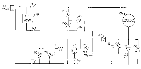
B ief_DescriPtion of the Drawinqs
The Figure shows a circuit diagram of the preferred
embodiment of the circuit for operating an elapsed time
indicating meter.
DescriPtion of the Preferred Embodiment
Turning now to the Figure, the schematic diagram o~
the preferred embodiment of the operational timer circuit of
the
~i6~5
present invention is illustrated, and includes terminals T1, T2 and
~3. Device 101, whose cumulative tlme of operatlon the tlmer cir-
cuit is to record, is operatively connected between ~he clrcui~s
input terminals T1 and T2. In the preferred embodiment, device 101
is an a.c. motor which draws current at a first predetermined level
when the motor is on and draws current at a second predetermined
level when the motor is under load. A switchable a .c. power source
is connectable to the circuit's input terminals T1 and T3.
The operational timer circuit includes resistor 102 connected
between input terminals T2 and T3 for detecting the current drawn
by device 101. In the preferred embodiment, resistor 102 has a small
resistance value to minimize the voltage drop across the reslstor.
Potentiometer 103 is connected full scale across resistor 102,
and the full scale voltage reading across potentiometer 103 is identi-
cal to the voltage reading across resistor 102. The potentiometric
terminal of potentiometer 103 adjustably controls the vol~age to
common base transistor 104.
Elapsed time indicating meter 105 is connected in series with
silicorl controlled rectifier (SCR) 106, the meter and SCR being cou-
pled across the circuit~s input terminals Tl and T3. As is well known
in the art,the SCR operates as a short circuit when ever current at
gate terminal 107 is positive. Absent a positive current value at
gate terminal 107, the SCR operates as an open circuit.
The voltage across potentiometer 103 is ad~ustable to apply a
range of voltages to common base transistor 104 such that a prede-
termined voltage of the amplified voltage across the potentiometer
will trigger the SCR. Thus, potentiometer 103 is adjustable to set
the threshold level which causes the SCR to conduct, thereby per-
mitting elapsed time indicating meter 105 to record the cumulative
time during which device 101 is operating at a specifled condltion.
The specified condition can either be at all times during whlch
devlce 101 is operating generally or, in the preferred embodiment, a~
al} times during which device 101 is operating under load conditions.
Load conditions, therefoI e, is detected by the circuit as the
increased current drawn by device 101 as seen by resistor 102.
The output of common base transistor 104 is rectified by diode
108 and filtered by capacitor 109. In the preferred embodiment,
resis~or 110 is included in order to limit the current drawn from the
collector of the common base transistor when the SCR turns on.
Likewise, resistor 111 is lncluded in the preferred embodiment in
order to limi~ the current in the line between the potentiometric
terminal of potentiometer 103 and the emitter of common base tran-
sistor 104.
Diode 112 is connected in parallel with the SCR to provide
bias current for the elapsed time indicating meter at all tlmes
except when the SCR is conducting.
Biasing for the common base transistor is obtained by resis-
tors 113 and 114, and the biasing voltage is kept relatively constant
and of one polarity by Zener diode 115, capacitor 116 and diode 117.
The common base transistor base bias is obtained by resistor 118 and
capacitor 119.
Although other circuit component values will be readily obvi-
ous to ~hose skilled in the ar~, the preferred embodiment of the
operational timer circuit shown in the Figure comprises component
values as follows:
Resistors 102, 103, 110, 1119 113, 114 and 11~ have reslstences
values of ~in Ohms) of 0.01, 100 (full scale), 20k, 220, 47k, 101c and
lM, respectively.
6~5
-- 9 - 72761-1
Capacitors 109, 116 and 11~ have values (in uf) of
3.3, 47 and 4.7, respectively.
Diodes 108, 112, 115 and 117 are part numbers lN914,
lN4006, 6.8 v Zener and lN914, respectively.
Common base transistor 104 is part number 2N2222
and, SCR 106 ~as a 0.84 400 PIV sensitive gate.
Elapsed time indicating meter 105 can be any device
which displays time in either hours, minutes, seconds or any
combination thereof, and can either be illuminating or non-
illuminating. In the preferred embodiment, meter 105 displays
illumina~ed time in hours and minutes, such as part number
T4A52R mini hour meter 4020 manufactured by EHM Company.
Although illustrative embodiments of the present
invention have been described in detail with reference to the
accompanying drawing, it is to be understood that the invention
is not limited to that precise embodiment. Various changes
or modifications may be effected therein by one skilled in the
art without departing from the scope or spirit of the invention.
For example, although the preferred embodiment is
shown for use with devices operating at standard United States
and Canadian a.c. power sources, circuit component modifica-
tions will be readily obvious to those skilled in the art for
applications with devices operating from different a.c. sources
voltages and/or frequencies.