Note: Descriptions are shown in the official language in which they were submitted.
~Z6~3~
BACKGROUND OF THE INVENTION _
Field of the Invention
The present invention relates to a circuit
arrangement for serial data transmission between a plurality
of subscriber stations, comprising at least two data
transmitters that have their output terminals connected to
one and the same data bus which comprises two leads,
respectively having a control input connected to a control
arrangement and being controllable such that at most one of
the data transmitters is activated at a given time, whereby
the data transmitters, in their activated conditions, emit a
voltage of a first polarity or a second polarity to the data
bus dependent on the state of a data signal applied to the
input, whereby the data transmitters have a higher internal
resistance at the output in the passive condition than in the
active condition, and whereby at least one data receiver is
connected to the data bus, the data receiver, in the manner
of a differential amplifier, assuming one o~ two prescribed
signal states at its output given an input voltage and
dependent on the polarity of the input voltage, and whereby
the data bus is loaded with an effective load between the two
leads at at least one location, the efEective load being of
such a nature that the voltage between the leads of the data
bus~has at least about the~value zero given nonactive data
transmitters. ~ ~
,
Description of the Prior Art
A circuit arrangement of the type generally set
forth above is already known rom the periodical "Elektronik",
6/23 March 1984, page 24 and 12jl5 ~une 1984 pages 97 and 98.
.
"
~ . .: - . -, .-
~%~i~i3~
The cited known circuit arrangement contains
interface modules for serial transmission, each of which is
composed of a data transmitter and a data receiver and is
suitable for full-duplex or half-duplex operation. ln half-
duplex operation, the output of the clata transmitter is
directly connected to the input of the data receiver in each
subscriber station~ The subscriber stations can be a computer,
for example, and peripheral devices connected thereto which
are connected to a data bus. The data transmltter and the
data receiver in each subscriber station can be driven into
an active condition or into a passive condition by control
signals.
Further~ the Data Book of Texas Instruments,
Interface Circuits, 1980 Edition, Page 388, discloses a
circuit arrangement comprising interface modules in which both
ends of the bus are terminated by a resistor having the value
of the characteristic impedance. In relationship to the
internal resistances at the output side of inactive data
transmitters, such a resistor is so small that the voltage
between the leads of the data bus has at least approximately
the value zero.
Since, in a circuit arrangement of the type set
forth a~ove, the data transmitters, in the active condition,
represent a low-impedance voltage source at their outputs
whose voltage is dependent upon the logic level of the data
signal applied to the respective input, only one data trans-
mitter can be active at a given time.
-- 2 --
.~
,.
.
~6~
To this end, the control signal that drives the
data transmitter of a subscriber station into its active
condition can be transmitted to all other subscribers and
can be used at the other subscribers to make an activation
impossible for the time in which the data bus is occupied.
It is thereby obvious to transmit control signals via a
i control line or via a control bus which is provided in
addition to the data bus.
SUMMARY OF THE INVENTION
-
The object of the present invention is to provide a
circuit ~rrangement as set forth above such thht a mutual
control of the subscriber stations occurs via the data bus
itsel~ without the assistance of additional control lines,
this mutual control being accomplished such that the subscriber
stations can access the data bus on their own when the bus is
not occupied by another subscriber station.
Given a circuit arrangement of the type set forth
above, all data transmitters are high-impedance devices at
their outputs given an unoccupied data bus. Proceeding from
the perception within the scope of the invention that the high-
impedance tristate condition is exploitable for control
purposes, the circuit arrangement for achieving the above
object is constructed in such a manner that it is particularly
characterized in that at~least one of the control arrangements
is preceded by a recoqnition circuit which outputs a free
signal at its output having a first logic state given at least
approximately identical voltages at the leads of the data bus
and outputs a busy signal having a second logic state to the
control arrangement given different voltages;at the lines of
the data bus ~ The data transmitters can thereby be connected
.~
- 3 -
., ., ~ , :
~ 2~
to the subscriber stations in unmediated or mediated fashion,
particularly by way of transmission devices that are provided
with modems.
The load with which the data bus is loaded at at
least one location can be ~ormed by terminating impedances,
input resistors of the recognition circuit and/or other load
resistors. In particular, the load is entirely, or partly,
composed of terminating impedances having the value of t.he
characteristic impedance of the data line with which the data
line is provided in view of a high bit rate of the data signal
t.o be transmitted.
The data t.ransmitters can be of such a nature that
they have, respectively, a positive potential in comparison
to a reference potential or ground at the one output terminal
and have a negative potential in comparison thereto at the
other output terminal. On the other hand, there are data
transmitters that, in their activated condition, have h first
prescribed voltage at one of the two output terminals and have
a second prescribed voltage, higher than the first prescrlbed
voltage and of the same polarity, with respect to the
reference potential at the other of the two output terminals,
so that differently-polarized output voltages likewise occur.
Data transmitters of interface modules that are conceived for
the interfaces RS485, RS422 and the like are, in particular, of
this.type. The interface RS485 i5 known for half-duplex
operation via a two-wire data bus and the interface RS422 is
known for full-duplex operation or half-duplex operation via a
~our-wire data bus.
An advantage which derives on the basis of the fore-
-- 4 --
,: ~
~Z~ 3~L~
going measures is that the subscriber StâtiOn can acquireinformation concerning the occupancy of the data bus with
structures that are slmple to realize without a separate
control bus being required for this purpose. With particular
advantage, the busy signal can be used for the control of
one or more modems such that the transmitter of the modem or,
respectively, the transmitters of the modems are driven into
the active or passive condition dependent on the occupancy of
the data bus. When a modem seizes the data bus, then the data
transmitters of all other modems are automatically activated
without the requirement of switch over device= comprising
involved control structures.
The recognition circuit can be forl~ed by an
unpolarized relay whose winding is connected to the two leads
of the data bus and which responds when a data transmitter is
active. Since the winding of the relay loads the data bus,
no voltage adequate for excitation ~ the relay can then build
up on the data bus when all data transmitters are inactive
and therefore comprlse a relatively high-impedance internal
resistance at their respective outputs. When, by contrast, a
da~a transmitter is active, then a voltage that constantly
changes in polarity in accordance with the data to be trans-
mitted occurs between the leads of the data bus. Since the
relay i5 not polarized, it then nonetheless re~ponds.
According to anotherlfeature of the invention, the
circuit arrangement is constructed in such a manner that it is
characterized in that the recognition circuit contains two
optocouplers whose inputs are connected to the data bus in an
anti-parallel manner and whose outputs ~re isodireotionally
;
, ~
connected in parallel, and in that the parallel circuit is
connected to a d.c. voltage source via a resistor, and in
that the series circuit of optocouplers and resistor is a
component portion of an evaluation arrangement which outputs
a free signal at its output having a first logic state given
identical logic levels at the inputs of the recognition
circuit and which emits a busy signal having a second logic
state to the control arrangement given unequal logic levels
at the inputs of the recognition circuit. The data bus is
thereby loaded such by the diodes of the optocoupler that,
given nonactive data transmitters at the data bus, no voltage
that could lead to a response of the optocouplers can build
up. When, by contrast, a data transmitter is active,then a
voltage having alternating polarity builds up on the data bus.
( Respectively one or the other optocoupler responds dependent
; on the polarity of the appertaining pulse.
In embodiments of the invention involving an
unpolarized relay or the two optocouplers in the recognitLon
circuit, the recognition circuits represent a load to the data
bus that guarantees a reliable operation ~ the recognition
; circuit. Under given conditions, additional load, particularly
terminating impedances, can be present at the data bus.
- When the data bus is provided with a terminating
; impedance at at leàst one location, then, in accordance with a
urther feature of the invention, the recognition circuit can
be formed by an EXCLUSIVE OR gate. The EXC~USIVE OR gate can
thereby be relatively high-impedance at its input.
:
;
' i. ' '
i3~
A subscriber station dare not access the data bus
when it has already been occupied by another subscriber.
When a subscriber station has seized the data bus, the
recognition circuit recognizes such seizure. In such a case,
howeverl the data bus continues to be available to the
subscriber station.
When the subscriber station itself does not contain
a device that prevents self-disconnection of the subscriber
station in ~he operating state under consideration, then it
is expedient to forward a busy signal to the subscriber station
only when the data bus is occupied by a different subscriber
station.
Since the data transmitters in the subscriber
stations are activated with the assistance o~ control signals,
these control signals make criteria available regarding
,
whether an identifiéd occupation of the data bus may possibly
occur from the appertaining subscriber station itself. A
common evaluation or lvgic operation of the control signal and;
of the busy criterion therefore permits a determination
regarding whether the data bus is occupied by the appertaining
subscriber station or by some other subscriber station.
; For this purpose, the circuit arrangement is
particularly characterized in that a control input of the
subscriber station preceding the assigned data transmitter is
respectively preceded~by~an~AND gate that has a first input
connected to~the recognition circuit and that has a second
input, ~ogether with the appertaining data transmitter
controllable by the subscriber~station such tha~ the AND gate
is Lnitialized only given a passively controlled data tr~ans-
-- 7 --
- ~ ., - - : .", ~ .
3~
mitter.
Dependent on the type of control circuit, with or
without following negation, th~ AND gate inhibits the
criterion "data bus occupied" when the appertaining sub-
scriber station itself seized the data bus.
An arrangement that advantageously eliminates
disturbances or, respectively, needle pulses arising due to
switching events is particularly characterized in that the
output of the evaluation device i5 connected to a Schmitt
trigger via an RC element.
An arrangement which is further characterized in
that the Schmitt trigger is constructed as an AND gate hâs
the advantage that the Schmitt trigger simultaneously
eliminates disturbances and realizes the desired AND operation
;~ or NAND operation.
;~
BRIEF DESCRIPTION OF THE DRAWINGS
~,~
Other objects, features and advantages of the
invention, its organization, construction and operation will
be best understood from the following detailed description,
taken in conjunction with the accompanying drawing, on which:
`~ ~ FIG. 1 is â schematic circuit diagr~m of a circuit
,
arrange~ent for serial data transmisslon between a plurality
of digital and transmission assemblies connected to one another
via a data bus and comprising recognition circuits containing
relays;
~; FIG. 2 is a schemâtic circuit diagram of a
recognition circuit having an optocoupler; and
,~ .
~ 8 -
-
Ei3~
FIG. 3 is a schematic circuit diagr~m of a
digital assembly of a circuit arrangement for serial data
transmission, the digital assembly comprising an EXCLUSIVE
OR gate in the recognition circuit~
DESCRIPTION OF_THE PREFERRED EMBODI~ENTS
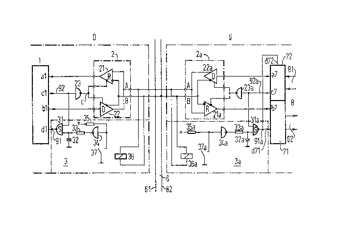
Referring to FIG. l, a circuit arrangement is
illustrated for serial data transmission. The two-wire bus 6
connects a plurality of hssemblies of a remote control
apparatus or of a remote control device, the digital assembly
D and the transmission assembly U thereof being illustrated
on the drawing. In addition to be used for data transmission,
the two leads 61 and 62 of the data bus 6 are also used for
the communication control signals that serve for the mutual
control of the assemblies.
The digital assembly D is a device for executive
sequencing and, as a subscriber station 1, contains a USART
device 1 controlled by a microprocessor, an interface module 2
and a recognition circuit 3.
The transmission assembly U comprises a modem 7
connected to a four-wire audio frequency line 8 which comprises
a ~ransmitter 71 and a receiver 72, and further comprises an
interface module 2a and a recognition circuit 3a. The modem 7
.
~is composed of, for example, an FM transmitter and an FM
~- receiver. The audio frequency transmission line 8 leads to at
~; least one further subscriber station and is a component of a
remote control~network comprising a plurality of stations or,
~,~
respectively, further subscriber stations in the example set
forth herein. The transmission line is a four-wire line
comprising an incoming line 81 and an outgoing line 82. A two-
~''
_ 9 _
. : .
wire line can be employed, when warranted, insteaa of the
four~wire line. In this case, the transmitter 71 and the
receiver 72 are to be connected to the two-wire line.
Further digital and/or transmission assemblies can
be connected to the two leads 61 and 52 of the bus 6. In
particular, such further digital asse~blies can be devices for
a status signal input or output. Further transmission
assemblies can serve the purpose of forwarding the serial data
onto the bus 6 by a digital assembly or by a transmission
assembly to further transmission lines and stations connected
thereto.
An interface suitable for such a multipoint bus
configuration serves as an interface between the assemblies
and the data bus 6, the data transmitters 22 or, respectively,
22a being high-impedance devices at their outputs in the
unactivated condition. In particular, the interface RS485 is
such an interface.
In a departure from FIG. 1, the data bus 6 can be
terminated at both ends by a respective resistor between the
two leads 61, 62 which has the characteristic impedance thereof.
All subscriber stations lie at a common ground potential by
way of a connection to the ground that is not shown on the
,: :
drawings.
~` For connection to the data bus 6, the assemblies, of
which the drawing illustrates one digital assembly D and one
transmission assembly U, are~each provided with a respective
interface module 2 or, respectively, 2a which, for example, can
~ be of the type SN75176a.
:~,
- 10 -
,, ,, ~ .
,
~ . .
~L~6~;3~1
In the interface module 2 of the digital assembly
D, the output terminals A and B of the dhta transmitter 22
are directly connected to the input terminals of the data
receiver 21. The terminal A is connected to the lead 61 and
the terminal B ls connected to the lead 62 of the data bus 6.
The data transmitter 22 and the data receiver 21
each have their control terminals connected to the co~non
control line C can be alternatively driven active and passive
by control signals, so that only the data transmitter 22 or
the data receiver 21 can be respectively active at one time.
The interface module 2a of the transmission assembly
U is constructed like the interface module 2 ~ the digital
assembly D. The output of the data transmitter 22a is
directly connected to the input of the data rece}ver 21a. The
i data transmitter 22a and the data receiver 21â each have
their control terminals connected to a common control line Ca~.
~^~ On the other hand, it can be advantageous in the
; digital àssembly D, to control only the data transmitter 22
via the control line C and to always leave the data receiver
.,
~ 21 switched on. Therewith, the data signal transmitted onto
:
~ ~ the bus 6 by the digital assembly D can be simultaneously
:. :
evaluated for supervision.
In the dlgital assembly D, the output of the data
reoelver 21 is connected to the data input al of the USART
device 1. The input o the data transmitter 22 is connected
to the data output~bl of the US~RT device 1. The control
~,
input of the data receiver 21 and the ~ontrol input of the
; data transmitter 22 are connected to another and to the control
, line C. The control outpu~ cl of the USART device 1 is
:~,
:,
.~:
;33L~
connected via an inverter 23 to the control line C of the
int.erface module 2.
The recogni.tion circuit 3 comprises an unpolarized
relay 36 whose winding is directly connected to the leads of
the data bus 6. The relay 36 comprises a contact 37 which
is a make contact connected to ground on one side and
connectible to a positive ~uxiliary voltage at the other side
via a resistor 35. The input of an inverter 34 is connected
to the junction of the contact 37 and the resistor 35. The
unpolarized relay 36 responds regardless of the direction of
the excita~.ion current.
The output of the inverter 34 is connected to the
signal input o a Schmitt triyger 31 via an RC element which
comprises a resistor 33 and a capacitor 32. A control input
of the Schmitt trigger 31 is connected to the control output
cl of the USART device 1.
The two inputs of the Schmitt trigger 31 are linked
to one another in the manner of an AND gate. The inverting
output of the Schmitt trigger 31 is connected to a control:
input dl of the USART device 1 via a control line 91.
The recogn~tion circuit 3a comprises an unpolarized
relay 36a whose winding is directly co.nnected to the leads of
the data bus 6. The relay comprises a contact 37a as a make
contact. This make contact is connected to ground on one side
and is connected to a positive auxiliary voltage at the other
~; side by way of a resistor 35a. The input of an inverter 34a
is connected to the junction of the contact 37a and the
resistor 3Sa.
- 12 -
' . ' .
~2~3~
The output of the inverter 34a is connected to a
signal input of a Schmitt trigger 31a via an RC element
comprising a resistor 33a and a capacitor 32a. A control
input ~ the Schmitt trigger 31 is connected to the control
output 7 of the modem 7.
The two inputs of the Schmitt trigger 31a are linked
to one another in the manner of an AND gate. The inverting
output of the Schmitt trigger 31a is connected to the control
input d71 and d72 of the modem 7 via a control line 91a.
An interface module of the type SN75176A or ~ 96176
can be employed, for example, as the data transmitter 21 and
the data transmitter 22 or, respectively, the data transmitter
21a and the data receiver 22a.
When the remote control station illustrated in FIG.
1 transmits, the transmission data are available at ~he output
bl of the USART device 1, are converted to the interface level
in the data transmitter 22 of the interface module 2 serving
as a driver, are fed via the lines 61 and 62 of the data bus 6
to the data receiver 21a of the interface ~odule 2a, are
converted to the TTL level by the latter and are output to the
input b7 of the transmitter 71 contained in the modem 7.
In the receiving condition of the remote control
station, the receiving data are avaiIable at the output a7 of
.,,
the receiver 72 contained in the modem 7, are converted to the
interface level in the data transmitter 22a o~ the interace
module, are fed via the leads 61, 62 of the data bus 6 to the
data receiver 21 of the interface module 2, are converted to
, .
~ the TTL level by the latteE ~nd are output to the data input
:;
al ~ the USART device 1.
- 13 -
.. .
.: . . : .
~ .
i3~
The tristate condition of the RS485 data bus 6
corresponding to a logic level "O" on a control line C or,
respectively Ca, signals the connected assemblies that they
can have access to the data bus. Wh~en an assembly accesses
the data bus 6, then the data bus assumes a non-tristate
condition. The evaluation of this condition leads to the
formation of a control signal in the further assemblies
which switches the control line 31 or, respectively, 91a to
the logic level "O" and thus inhibit access of all other
assemblies to the bus. This control signal also drives the
transmission assembly (assemblies) such that their transmitters
71 becomes active toward the transmission line 8 and such that
their receivers 72 are inhibited.
The US~RT device 1 can be, for example, of the type
; SAB8251A.
The control of the interface module via the bus 6
comprises the following operatlng conditions.
~` a) When the data bus 6 is not occupied, i.e.
, ,
when all data transmitters 22, 22a are in the
high-impedance tristate condition, the two
leads 61 and 62 of the data bus assume an
approximately identical potential since they
are connected to one another via the resistance
of the relay 36. This resistance, potentially
in combination with a further load, is
,~
~ comparatively a low impedance with respect to
:-.
the extremely high-impedance output resistances
~ of inactive data transmitters, even given a high
; number of windings~ The relays 36, 36a are in
:
~ - 14 -
, . . .
the idle condition and their contacts 37,
37~ are opened.
A volt~ge th~t corresponds to the logic level "1"
thereby respectively occurs at the input of the complimentary-
metal-oxide-semiconductor (CMOS) inverters 34 and 34â. The
output ~ the Schmitt trigger 31 or the Schmitt trigger 31a
is therefore swi.ched to the logic level "l'/ regardless of the
logic level of the control signal applied at its control
input.
In the digital assembly D and, under given conditions,
in further digital assemblies, the logic level "1" on the
control line 91 siynals the USART device 1 that the data bus
is not occupied. In this case, the audio frequency transmissicn
line 8 of the remote control network is also not ~ccupied. In
,:
~ ~ the transmission assembly and, under given conditions,~in
,
furth~r transmission assemblies, the logic level "l" on the
control line 91a drives the receiver 72 for reception and
-
inhibits the transmitter ~l.
b) When the data bus 6 is seized by the digital`
assembly, then, in the seizing digital assembly,
the control output cl of the USART device l
swltches the contr~ol line 92 ~o the logic level
"0". The inverter 23 actlvates the data trans-
mitter~22.~The output of the dat~ transmitter
22 is~therefore~ln~a low-impedance state.
Dependent on the logic state at the data outputs
bl of the~SART devioe l, a logic lavel "l" or
a logic~level "0" is transmitted via ~he data
bus 6.
: ~
- 15 -
,~
,. :.. .~ , . .
63~
The two prescribed voltages that ~he output
terminals A, B of the daka transmitters 22, 22a can assume
relative to the reference potential have the same polarity.
In the case of the interface RS485, the volt~ge 3.7V, for
example, lies at the output terminal A of the interface
module 2 given the logic level "1" and, for example, the
voltage l.lV with respect to ground lies at the output
terminal B. Given the logic level "O", the voltage l.lV,
for example, lies at the output terminal A and the voltage
3.7V, for example, lies at the output terminal B . Given an
activated interface module and a bus 6 thereby occupied, one
of the two leads 61 or 62 therefore fundamentally lies at the
low potential of, ~or example, l.lV and the other lead lies
at the high potential of, for example, 3.7V. The voltage
difference causes the relay 36a to respond. In all assemblies,
therefore, the outputs of the inverters 34 or, respectively ~.j
34a switch to the logic level "1".
In ~he active digital assembly D, this signal is not
transmitted since the Schmitt trigger 31 is inhibited by a
logic level 170" from the control output cl of the USART device
`;: ~
In the operating conditions under consideration,
further digital assemblies~(not shown on the dr~wing) that may
be present, by contrast, are~not actlve, so that;the Schmitt
triggers are y by the logic level "1". The logic level
"l" at the output of~the inverter therefore drives the;control
line to~the logic level IlOn: via the following Schmitt trigger,
informs the USART devi~e that the data bus 6 is occupied by
~ another assembly and therefore inhibits aCGess to the data
': ~
- 16 -
~'~
.: ' .' : : ., ~ :
bus 6.
In the transmission assembly U and, under given
;conditions, in further transmission assemblies, the logic
level "1l' at the output of the inverter 34a drives the
: control line 91a to the logic level "O" via the following
Schmitt trigger 31a, thus inhibiting the receiver 72 and
switching on the transmitter 71.
c) When the data bus 6 is occupied by the
; transmission assembly U, then the receiver
72 receives a message from the remote
control network via the audio frequency line
8. The control line 92a switches to the
logic level "O", thus inhibiting the Schmitt
~rigger 31a and activating the data trans-
:
mitter 22a via the inverter 23a so that the
data transmitter 22a works onto the data
bus 6. The analogous case applies to a
- further transmission assembly in case it
occupies the data bus 6 instead of the
- transmission assembly U.
In the digital assembly D connected to the data bus
: ~6, the relay 36 re~ognizes the busy condition and the inverter
~: : 34, with a logic level "O" that proceeds to the control signal
; input dl of the USART device 1 via the control line 91,
inhibits the access of the USA~T device 1 to the bus 6. The
same is true of further digital assemblies that may be connected
: to th~ bus 6.
When further transmission assemblies U are connected
to the bus 6, then the relays thereof recognize the busy
:
- 17 -
;3~
condition and the inverter 34 or, respectively, 34a switches
off the receiver 72 and switches on the data transmitter 71
via the following Schmitt trigger 31 or, respectively, 31a.
Branching functions in transmission networks can be
realized in a particularly simple manner with the assistance
of the circuit arrangement without having additional logic
operations or control signal lines required between the
transmission assemblies.
In a modification of the illustrated circuit
arrangement, it can also be advantageous not to drive the
receiver active or passive dependent on the occupancy of the
data bus, but t:o always maintain the receiver .ready to receive
in that its control input is permanently applied to ground
potential.
FIG. 2 illustrates a recognition circuit that can
be employed in the circuit arrangement for serial data
transmission as illustrated in FIG. 1, instead of the
recognition circuit 3 or, respectively 3a. ~he recognition
circuit 3 of the digital assembly D comprises, in FIG. 2,
optocouplers 38 and 39 whose inputs are connected in anti-
parallel manner to the lead 61 and 62 of the data bus 6 via a
resistor 40. The outputs of the output couplers 38 and 39
are connected to ground at one termin~l and are interconnected
in the manner of an:OR gate and connected to the input of the
inverter 34.
When data are txansmitted via the data bus 6 one
of the two diodes connected in antiparallel fashion respectively
.
~ responds, the one at a signal cond.ition and the other at a
,~
` disconnect condition. When one o~ the two optocouplers is
:'
- 18
: . : ,
;3~
through-connected, then the inverter 34 reports that the
data bus 6 is occupied.
Given the circuit arrangement for serial data
transmission of FIG. 3, only one digital assembly and the
data bus are shown. Further digital or transmission assemblies
occur from the assemblies shown in FIG. 1 in that a recognition
circuit of FIG. 3 is employed as the recognition circuit 3 or,
respectively, 3a. The recognition circuit 3 of FIG. 3
comprises an EXCLUSIVE OR gate 41 whose inputs are respectively
connected to the leads 61 and 62 of the data bus 6 via
respective resistors 42 and 43. The output of the EXCLUSIVE
OR gate 41 is connected to the Schmitt trigger 31 via the RC
element 32, 33.
- A pair of resistors 51 and 52 are connected to the
data bus 6. These resistors are dimensioned such that the
Ieads 61 and 62 of the data bus assume practically the same
; potential given passive data transmitters. Particularly
serving as resistors 51 and 52 are terminating impedances
which, preferably at the end of the line in the subscriber
stations, terminate the data bus with its characteristic
~; ~ impedance 1~ a known manner in order to enable a data trans-
mission with a comparatively high bit rate. The EXCLUSIVE OR~
g~te is, in particular, a CMOS logic element that, as such,
has comparatively high-impedance inputs and whose switching
level at the inputs lies;at about half the supply voltage
which, in particular, lies at 5V.
- When both leads 61 and 62 of the data bus 6 have
: ~ .
the same potential, then the E~CLUSIVE OR gate recognizes that
the data bus 6 is free. When the potentials at the data
- 19 -
--, ~ :, . -
., ;- .
~26~3~
lines 61 and 62 differ from one another, then the EXCLUSIVE
OR gate reports th t the data bus 6 is busy.
Although we have described our invention by
reference to particular illustrative embodiments thereof,
many changes and modifications of the invention may become
apparent to those skilled in the art without departing from
the spirit and scope ~ the invention. We therefore intend
to include within the patent warranted hereon all such
changes and modifications as may reasonably and properly be
included within the scope of our contribution to the art.
~' :
~ '
~. :
. ::
:
,: :
"~;
~' '
:` :
: - 20 -
,