Note: Descriptions are shown in the official language in which they were submitted.
-- 1. --
The present invention relates to a digital image
processing system.
An image processing system, such as a digital copier
or a -facsimile system has been recently proposed, having
an accumulating transducer element such as a solid state
image pick-up device, e.g., a CCD for reading an image
and converting an analog signal into a digital signal.
~he digital signal obtained is processed and is trans-
mitted through a digital transmission line or is used to
reproduce an image through a laser beam printer or the
like.
In order to transmit and accumulate image signals,
such a digital image processing apparatus requires special
processor, transmitter and storage elements, which re-
quires image processing equipment additional to otherinformation processing equipment for word processing or
other computer functions, thus increasing the amount of
hardware competing for limited narrow office space,
complicating installation, and increasing costs.
Methods are known for compressing and expanding
digital image data so as to reduce the amount of data to
be transmitted. In a digital recording apparatus,
requirements for high speed and high image quality to-
gether with an increase in the amount of data to be
handled, mean that high speed image signal processing
- 2 ~
must be performed, and i-t is therefore technically
difficult to compress, expand, transmit and read the
digital image signals in real time.
Furthermore, depending upon particular patterns
being processed, it is possible for the amount of image
data to be actually increased upon data compression.
For example, in Modified ~uffman one dimensional run
length coding, 2 adjacent bits of data representing 1
black bit and 1 white bit are converted into 9 bits of
data upon coding. This increased amount of data may ex-
ceed the transfer capacity of a transmission line or
occupy the line for an excessive time.
When the pel density or image processing speed
differs as between an image reader and an image recorder,
connection of the image reader with the image recorder
for exchange of the digital image data becomes very dif-
ficult or impossible.
It is an object of the present invention to provide
an image processing system which addresses certain prob-
lems described above, and to provide an informationprocessing apparatus which can perform both image proces-
sing and other information processing, which information
processing is not necessarily associated with the image
processing, thus providing the functions of a computer
system.
According to the invention there is provided an image
processing system comprising a computer bus line; image data
processing means including means for transferring image data,
structured as a succession of distinct data units, between
said image data processing means and said computer bus line
intermittently unit by unit; information processing means
connected to said bus line; and means enabling said
information processing means to use said bus line during
transfer of image data in a time period when said bus line is
unused between intermittent transfers of said units of data
by said image data processing means. The image data
processing means may either generate image data which is
transmitted to the bus line or process data received from the
bus line.
The above and other features of the present invention
will become apparent from the following description taken in
conjunction with the accompanying drawings, in which:
Fig. 1 is a system block diagram showing an image
processing system according to the present.........
6~
1 invention;
Fig. 2 composed of Figs. 2A, 2B and 2C is a
detailed circuit diagram of the RP adapter in the
system according to the present invention;
Figs. 3, 4 and 6 are timing charts for explain-
ing the operation in the system of the present
invention;
Figs. 5a, 5b and 5c are diagram showing the
transmission data;
Figs. 7-1 to 7-3 are flow charts for explain-
ing the data transmission in the system according to
the present invention; and
Figs. 8-1 and 8-2 are representations for
explainingthe use states of the bus in the system
according to the present invention.
DETAILED DESCRIPTION OF THE PREFERRED EMBODIMENT
The preferred embodiment of the present
invention will be described below.
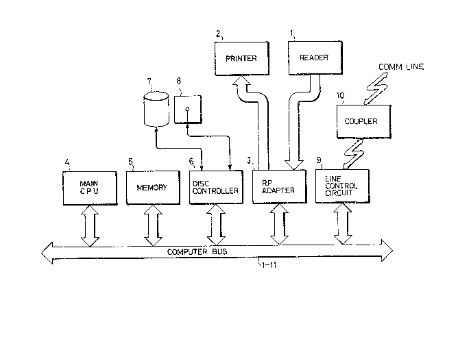
Fig. 1 is a system block diagram to which an
image processing system according to the present
invention can be applied.
A reader 1 reads an original with a CCD image
sensor, performs an A/D conversion, a shading
correction, and a digitizing processing and the like,
and produces a digital image signal to an external
circuit.
-- 5
A printer 2 forms on a printing paper sheet a digital
image and is, for example, a laser beam printer (LBP).
The reader 1 and the printer 2 can be directly coupled
to each o-ther to constitute a copier. According to the
emhodiment of the present invention, the reader 1 and
the printer 2 are connected through an interface to
additionally provide a facsimile function without requiring
much modification in the reader 1 or the printer 2.
An RP adapter 3 is a converter which converts the
digital image signal exchanged between the reader 1 and
the printer 2 into a signal which can be easily handled
by a computer hus 1-11. The computer bus 1-11 can be
the MULTIBUS (Trade Mark) bus system available from Intel
Corporation and has a maximum transmission rate of several
Mwords/sec. A main CPU 4, a memory 5, a disc controller
6, a line control circuit 9, and the RP adapter 3 in
the forms of boards are connected to each other through
the computer bus 11.
Original image data read by the reader 1 is converted
by the RP adapter 3 and is stored in the memory 5. The
data is, if required, stored in a magnetic disc 7 or
floppy disc 8 through the disc controller 6. The stored
data is sen-t onto the communication line through the
line control circuit 9 (modem or the like~ and a coupler 10.
The original data received through the
communication line is stored in the memory 5 through the
coupler 10 and the line control circuit 9 and is then stored,
if required, in the magnetic disc 7 or the floppy disc 8
through the disc controller 6. The stored data is sent to
the printer 2 through the RP adapter 3 to print an image on
a printing paper sheet.
A series of facsimile operations as described above
is controlled by the main cPu 4 in a centralized manner.
Figs. 2A, 2B and 2C from a circuit diagram of the RP
adapter 3 of the system shown in Fig. 1. Referring to Figs.
2A and 2B, reader 1-1 transmits serial digital image data for
each read line together with a sync signal. The reader 1-1
performs a main scan with a 1-line CCD and a sub scan by
moving one of the CCD and an imaging system at a
predetermined speed relative to the other. The reading
operation is performed at a resolution of 400 bpi (bit/inch)
in both of the main and sub scan directions.
A data compressor unit or data compression unit 1-2
compresses image data Video of the bit format from the reader
1-1 by an encoding or other technique. In this embodiment,
a known run length coding circuit is used. A serial-to-
parallel converter (to be referred tc as an S ~ P converter
hereinafter) 1-3 converts the bit serial image data Video
into parallel data. Double buffer memories (RAMs) 1-4
and 1-5 and 1-6 and 1-7 have capacities to store one-line
image data obtained throuyh the data compressor unit 1-2 and
the S ~ P converter 1-3. The buffer memories are operated
such that while the image data is written in the memory 1-4
5 (1-6), the image data is read out from the memory 1-5 (1-7).
Write address counters 1-8 and 1-9 count data write addresses
for the respective double buffer memories. A comparator 1-
10 compares the magnitude of the converted data from the
image compressor unit 1-2 with that of the converted data
from the S ~ P converter 1-3. An output from the comparator
l-10 controls selector 1-26 so as to supply whichever
converted image data has the smaller data magnitude to a
MULTIBUS (computer bus) l-11. The converted image data is
supplied to the memory and other modules shown in Fig. 1
through the computer bus at a predetermined computer system
speed.
The section for decoding or restoring the compressed
image data shown in Figure 2C, has the following
configuration. Double buffers 1-30 and 1-31 are for
synchronizing the data transfer from the computer bus 1-11,
which provides a source of compressed data, and readout of
the compressed data by restoration logic. A data request is
generated on the computer bus 1-11 in synchronism with a read
address counter 1-41. Decoder select logic 1-32
discriminates the properties
of the compressed data read out from the double buffer and
selects a restoration logic to be used. A data restoration
unit 1-33 performs a function complementary to that of the
data compressor unit 1-2. A parallel-to-serial converter
(to be referred to as a P ~ S converter) 1-34 performs a
function complementary to that of the S -~ P converter 1-3.
In accordance with the restoration logic utilized, a
RAM 1-35 receiving the restored data allows readout of the
restored bit serial image signal and conversion of pel
density in the sub scan direction. An output from the RAM 1-
35 is reproduced by a printer 1-45.
In this embodiment, compression of the image data is
performed in synchronism with a sync signal HSYNC
corresponding to a 1-line read signal from the reader 1-1.
Restoration of the image is performed in synchronism with a
sync signal D-HSYNC (corresponding to a l-line beam scan end
in an LB printer) from the printer 1-45. When the sync
signal supplied to the compressor or restoration unit is
gated and is supplied thereto, pel density conversion, image
enlargement and reduction can be performed. The sync signal
gate means for this purpose is an HSYNC video enable gate
logic 1-12 ox a D-HSYNC gate logic 1-36.
The mode of operation of the system of this
embodiment will be described below.
Compression Circuit
The circuit portion shown in Figs. 2A and 2B to the
left side of the
1 alternate two iong and one short dashed line in
Fig. ~ is a compression circui-t. A digital image
signal from the reader 1-1 is proces.sed and
transferred to the computer bus 1-11. Fig. 3 shows
an output signal from the reader 1--1 and a signal
format thereof.
The signal from the reader 1-1 consists of
a signal HSYNC as an internal signal for each line,
an image data transfer clock Video Clock, a serial
image signal Video, and a signal Video Enable which
indicates that the image signal is effective in a
l-line interval between the current and next signals
HSYNC.
The signal HSYNC corresponding to one clock
time is generated in synchronism with the signal
Video Clock. The reader used inthis embodiment has
a maximum main scan length of 8(1/2) inches and a
resolution of 400 bps. Therefore, 3,400-bit image
data is transmitted as l-line image data. Therefore,
the invertal (image effective interval) of high level
of the signal Video Enable corresponds to 3~400
clocks Video Clock.
These signals are supplied to the data
compressor unit 1-2 and the S ~ P converter 1-3
which independently prepare parallel data. The coded
data from the data compressor unit 1-2 is written in
the double buffer memories 1-4 and 1-5, while the
1 parallel data from the S ~ P converter 1-3 is written
in the double buffer memories 1-6 and 1-7. The write
address counters 1-8 an 1-9 control the write
operation in the double buffer memories 1-4 to 1-7.
Each counter is initialized by the signal Video
Enable. The counter 1-8 is operated by the clocks
synchronized with the image coding by the data
compressor unit 102. The counter 1-9 is operated by
the clocks synchronized with the conversion operation
of the S , P converter 1-3. The switching operation
of the double buffers is performed by the address
selectors or data selectors 1-18, 1-19, 1-20, 1-21,
1-22 and 1-23 when a toggle flip-flop 1-13 changes
its state for each line. The read address data is
supplied from the computer bus through an address
buffer 1-29. Each buffer is thus read in synchronism
with data onthe computer bus and the readout data is
transmitted.
The circuit operation of the compressor unit
described above is illustrated in the timing chart
shown in Fig. 4. The S ~ P converter 1-3 converts an
image signal into a 14-bit parallel signal. There-
fore, the S ~ P converter 1-3 supplies one clock
signal to the write address counter 1-9 upon
receiving 14 clocks Video Clock. In this case, the
address counter counts from 0 to 42 in accordance
with 3,400 clocks Video Clock per line. The 3,400
i6~
- ~3 -
1 clocks Video Clock correspond to a memory capacity of
256 words. When the resolution is reduced to half,
and a serial-to-parallel conversion at a rate of 200
bpi is performed, the count of the address counter is
changed upon reception of 28 clocks and is incremented
to 122 upon reception of 3,400 clocks Video Clock.
In thls manner, -the S ~ P conversion address counter
1-9 performs a normal counting operation- within one
main scan period. However, the write address counter
1-8 for run length compression data operates in a
different manner. The image compressor unit 1-2
encodes the number of clocks Video Clock which were
held in one state and supplies a corresponding signal.
Therefore, the clock input to the write address
counter 1-8 changes every time the state of the clock
Video Clock changes. Therefore, when a 3,400-bit
image signal of one line is received, 3,400 clocks
are received in the address counter 1-8. In other
words, while the output from the address counter 1-9
is kept at a predetermined value, the output from the
counter 1-8 changes from 1 to 3,400. Which one of the
conversion data from the unit 1-2 and the converter
1-3 is smaller than the other is discriminated by
comparing the counts of these address counters. The
conversion data amount is determined by the trailing
edge of the Video Enable. Therefore, the counts from
the address counters are latched in flip-flop 1-14
I ? ~65~
- 14 -
1 and 1-15. The values from the respective flip-flops
1-14 and 1-15 are compared by the comparator 1-10,
an output fromwhich is latched in a flip-flop 1-25
in response to a line sync signal HSYNC. Depending
upon the output state of the flip~flop 1-25, the
selection of the data to be read onto the computer
bus 1-11 is performed by a selector 1-26. When the
number of clocks received by the address counter 1-B
counting the run length exceeds a capacity (256
words)on the memory, the selector 1-26 is set to
select data from the S ~ P converter 1-3 in
accordance with the other input signal to an OR gate
1-24.
The data written inthe buffer RAMs 1-4 to
1-7 will be described with reference to Fig. 5. One-
line data from the unit 1-2 and the converter 1-3
are sequentially written at addresses 2, 3 and so on
in 16-bit parallel data starting from address 1 of
the RAMs 1-4 to 1-7. The data has the following
format.
In the case of the run length coded data
from the compressor unit 1-2, the data is written as
shown in Fig. 5a. The data from the S ~ P converter
1-3 is written in the RAMs 1-6 and 1-7, as shown in
Fig. 5b. In this case, "00" at the 14th and 15th
bits indicate that bits 0 to 13 are image data.
When write of one line data is completed, an
13 --
identification code for a start of one line is added to the
counts of the addresses latched in the flip-flops 1 14 and 1-
15, and the results are written at address 0 of the RAMs.
The format for this data is as shown in Fig. 5c. More
specifically, "1" is written at the 13th bit of the data
written at address 0 of the RAMs 14 and 15, and "0" is
written at the 13th bit of the RAMs 1-6 and 1-7. The 15th
and 14th bits are identification code which identifies if the
data is data at the bovndary between lines or actual image
data.
In this manner, the unit 1-2 and the converter 1-3
independently write the conversion data in the RAMs in
response t~ the sync signal generated for each line.
How~ver, only one of these data is read out, and selection
between these data is determined in accordance with the
counts of the address counters 1-8 and 1-9 during the write
operation.
In response to an interrupt signal generated by the
signal HSYNC, the computer bus 1-11 starts reading the
conversion data from the preceding line which is written in
the RAMs. The read rate must be fast enough to allow read
out of the effective data in the RAMs within one interval of
the signal HSYNC. The computer bus 1-11 sends a data read
request signal from an interrupt request logic 1-2-/ to the
main C~U 4 or the disc controller 6 which responds to the
received signal and produces the read address data. Thus
data is read onto the bus starting from address 0 of the
- 14 -
selected RAM. At the address O is data indicating the type
and length of data of which the line is formed, which data is
stored at the addresses following address 0. Thus, the data
corresponding to this length is read, and the read data is
supplied to the memory devices 5 to 8 or the line control
circuit 9. In this case, the data length is determined by
the CPU or the disc controller 6 whieh eontrols the output of
the read address data. Then, unnecessary data need not be
read from the RAMs, and the occupation time of the computer
bus by the image data can be minimized.
A vacant time slot can thus be made available for
each one line during transmission of compressed data, and the
computer bus can be released for this a time.
The computer bus can be utilized during this vaeant
time for communication of data to or from the disc controller
6 by the line control eireuit 9, as will be described in more
detail below.
Fig. 7 is a flow chart showing data processing by the
main CPU 4 shown in Fig. 1. Fig. 7 1 shows a main routine
for storing computer data or wordproeessing data from the
eommunication line to the dise through the computer bus. The
main CPU 4 has a DMA controller. When ths DMA controller is
active, data received from the communieation line is stored
in the discs 7 and 8 or the memory 5 without going through
the CPU 4 or the data is read from the discs 7 and 8 and the
memory 5 to the communication line without going through the
CPU .
- 15 -
In the flow chart shown in Fig. 7-1, in step S-l, it
is determined whether the data received from the
communication line is stored to the full capacity of the
buffer in the line control circuit 9. When it is determined
in step S-l that the buffer is full, the DMA controller is
operated to transfer the line data in the buffer to the disc
controller 6 throuyh the bus 1-11. The line data is thus
written in the discs 7 and 8, in step S-2. Thereafter, steps
S-1 and S-2 are repeated to sequentially store the data
received through the line in the discs. Furthermore, since
the buffer is used, no problem occurs even if the data
transfer rate on the bus is different from the data transfer
rate on the communication line. When data is transferred
from the disc to the communication line through the bus, it
can be easily achieved with the buffer of the disc controller
6 and the DMA transfer, as shown in Fig. 7-1. Note that word
data from a wordprocessor or the like (not shown) connected
to the bus 1-11 can similarly be stored in the discs and
memory.
In this manner, the computer bus 1-11 can transfer
image data between the reader 1 and the printer 2 while it
transfers other information not related to the image data, or
word processing data, to the discs or to the line modulator.
Fig. 7-2 shows an interrupt routine for fetching the
image data from the reader 1 onto the bus 1-11. During this
routine, the bus is occupied for this purpose and is then
released.
- 16 - ~ ~ ~6~
When the interrupt request logic 1-27 shown in Fig.
2 generates an interrupt request signal, the CPU 4 takes
control of the DMA controller and interrupts data transfer as
shown in Fig. 7-1 between the communication line and the
discs through the bus l-11 (step S-3). Next, the CPU 4
supplies the read address data for reading out data from the
RAMs 1-4 to 1-7 shown in Fig. 2 to the buffer 1-29 so as to
read out data at address 0 of the RAMs and recognize the
amount of image data representing 1 line and stored in the
RAMs (step S-4). The recognized amount of the 1 line image
data is set in the DMA controller, and data transfer from
the RAMs of the RP adapter 3 by DMA is started (step S-5).
It is then determined (step S-6) in accordance with the data
amount set in the DMA controller if the data transfer of the
1 line image data has been completed. Thereafter, data
transfer between the communication line and the discs is
resumed in step S-7, as shown in Fig. 7-1.
Fig. 8 shows the occupation of the computer bus.
Fig. 8-1 shows the state of the bus in the flow diagram shown
in Fig. 7-2. "A" represents the period for which the bus is
occupied by data transfer between the communication line and
the disc, and "B" represents the period it is occupied by
data transfer between the RP adapter 3 and the memory 5.
Note that the memory 5 can store data corresponding
to several pages of normal documents. It is thus possible
for the main CPU 4 to perform editing such as partial
cancellation or synthesis of data held in the memory 5.
- 17 -
It is also possible to release the bus for data
transfer to or from the RP adapter only after a predetermined
data transf~r between the communication line and the disc is
completed. This may be achieved by giving a low priority to
the interrupt request logic 1-27 so that no interrupt is
allowed during the "~" bus occupation period. In this case,
the reader 1 displays that the bus is in the period "A" and
the read input is inhibited, so that the operator may not
perform a further read scan of the document. When the RAMs
shown in Fig. 2 are page memories capable of storing all the
information on the document, further input of the document
information can also be allowed in the period "A", a scan
operation of the document by the reader 1 is allowed, and a
full page of data is stored in the RAMs. However, readout of
the data from the RAMs onto the bus is inhibited. In the
periods "A" or "B", transfer will not be interrupted.
Therefore, data which requires continuous transmission can be
conveniently transmitted.
The configuration of the RP adapter shown in Fig. 2
is suitable when the image read speed of the reader 1 is
substantially the same as the data transfer speed of the bus
but is slightly slower than it. When the read speed of the
reader is very fast, RAMs having a capacity to store one page
of data must be used as RAMs 1-1 to 1-7.
j
- 18 -
Pel Density Conversion I
Conversion of pel density of compressed data will be
described below. Reduction of image data can be performed,
and a recording apparatus having a small recording pel
density can be used for an image reader.
When an original image to be read is a character
image or the like, a high resolution of 400 bpi is not
required. In such a case, if the resolution is lowered, the
transfer ti~e is shortened, the occupation time of the
computer bus can be reduced, and the efficiency of use of
intermediate buffer memory facilities such as discs and
memories is improved, resulting in an economical advantage.
When an image reduction function is not included in an image
recorder, the data must be compressed and then be transmitted
by the transmitter. If the recorder has an enlarging
function and the transmitter reduces the data and sends it,
the amount of data transmitted can be reduced.
The resolution in the main scan direction can be
decreased by a conventional method. According to this
method, the frequency of image sampling clocks is changed.
More specifically, the frequency of the clock Video Clock
corresponding to serial data Video before conversion at the
unit 1-2 and the converter 1-3 is controlled. The clock rate
is set as EMl in this case.
An HSYNC video enable gate logic 1-12 is used to
reduce the image in the main scan direction (to lower the
resolution). The image data compression circuit described
-- 19 --
above ls controlled by signals HSYNC and Video Enable.
Therefore, when these signals corresponding to data of
predetermined lines corresponding to a desired rate are gated
and not supplied, the data of these lines are not processed,
thereby sampling the data. Since a data read request ~ata
Req corresponding to these lines is not supplied to the bus
1-11, the data of the gated lines will not be`read nor sent
onto the bus.
In order to obtain data of a desired resolution, the
gate logic 1-12 has the following configuration. The gate
comprises a clock sampling means such as a 7479 TTL logic
chip which receives a signal HSYNC as a 1 line sync signal at
a clock terminal and generates a gate signal, thereby
sampling the signals HSYNC and Video Enable. The sampling
rate for determining the resolution (reduction ratio) is set
at EM2 by a setting means such as a switch (not shown). The
pel density and reduction ratio in the vertical and
horizontal directions can be arbitrarily set by independently
setting EMl and EM2.
Restoration or Expandin~ Circuit
The method of restoring the compressed data into
original data (expanding) will be described below. The
restoring unit restores the data supplied through the
computer bus 1-11. The compressed data is supplied from the
compression circuit described above but need not be that from
the compressor unit 1-2 connected to the same computer bus to
-- ~0 --
which the restoration unit is connected. The data stored in
the memory 5 can be data from the coupler 10.
First, the computer bus 1-11 writes a predetermlned
amount of data in one of RAMs 1-30 and 1-31. In this
embodiment, the RA~ has a capacity of 256 words. The RAMs 1-
30 and 1-31 comprise double buffers, such that when data is
being written in one RAM, the data is read out from the
other. The decoder select logic 1-32 supplies a clock to the
read address counter 1-41 so as to find an identification
code for each line from data stored in the RAMs. When the
identification code of a line is found, since the data format
(Fig. 5) of the subsequent data is written therein, a signal
is supplied to a selector 1-44 so as to select a
corresponding decoder. Data restoration is started in
synchronism with a sync signal G-HSYNC (to be described
later) from a printer 1-45. The data restoration circuit
has, in correspondence with the data compressor unit 1-2 and
the P - S converter 1-3, a data restoration unit 1-33 and a
parallel-to-serial converter (to be referred to as a P ~ S
converter) 1-34 for converting the parallel data into serial
data. The unit 1-33 and the converter 1-34 are normally
operated in response to the sync signal G-HSYNC. Each of the
unit and the converter generates a data request signal Data
Req requesting the next data in response to the restoration
operation. The decoder select logic 1-32 sends the request
signal from the restoration circuit designated by the line
interval signal as a clock for the read address counter 1-
,4,it- 21 -
41. In this manner, a line serial video signal is suppliedto the printer 1- 45. This is shown in Fig. 4. A clock D-
Video Clock from a clock generating means 1-42 ls generated
in response to a sync signal D-HSYNC from the printer 1-45,
and a serial image signal a D-Video and a D-Video Enable are
produced in response thereto.
The decoder select logic 1-32 sends a data request
signal from the restoration unit to the read address counter
1-41 to fetch the next data. However, if the received data
is a ]ine interval signal, the data is not supplied to the
restoration unit and the next line sync signal D-HSYNC is
awaited. Then, the data selector 1-40 is set in a
predetermined state and the next data is supplied to the
restoration unit.
When data read out from one of the double buffers is
completed (empty), the counter 1-41 supplies a count up
signal to a toggle flip-flop 1-37 so as to switch the read
and write operations of the two RAMs. At the same time, in
order to transfer 256 word data, the counter 1-41 supplies a
count up signal for 256 addresses to the interrupt request
logic 1-27.
Since a maximum data amount per line is about 256
words, the period of the interrupt signal supplied to the
computer bus 1-11 becomes longer than the interval of the
one-line sync signal D-HSYNC from the printer 1-45.
Therefore, a computer bus system having a minimum transfer
speed of 256 words per line period must be used, and the
faster the bus speed, the longer the empty time per line
after transfer of the 256-word data during which other
information processing and transmission can be performed.
This will be described with reference to Figs. 7 and
8. Fig. 7-3 is a flow chart of an interrupt routine for
transferring image data to the printer 2. When the interrupt
request logic 1-27 produces an interrupt request signal, the
CPU 4 interrupts the data transfer as shown in Fig. 7-1
between the communication line and the disc Via the control
bus 1-11 by taking control of the D~ controller (step S~8).
The amount of data, up to 256 words, to be stored in the RAMs
1-30 and 1-31 is set in the DMA controller. The write
address data for writing the image data in the RAMs 1-30 and
1-31 next is supplied to the address buffer 1-2~, shown in
Fig. 2. Then, data transfer from the memory 5 to the RAMs of
the RP adapter 3 by DMA is initiated (step S-9). Completion
of data transfer is determined by the amount of data set in
the DMA controller and the transfer of data from the memory
5 to the RAMs is then stopped (step S-10). Data transfer
between the communication line and the disc is then resumed
(step S-11).
Fig. 8-2 shows the usage of the bus during execution
of the flow chart shown in Fig. 7-3. A period A corresponds
to data transfer between the communication line and the disc,
and a period C corresponds to transfer of printing data from
the memory 5 to the RP adapter 3.
~ 3~
- 23 --
When the data transfer between the communication line
and the disc is completed, the interrupt request logic 1-27
is enabled and the bus can be released for transferring the
printing data. In thls case, the busy period "A" is
displayed at the printer display section of the main CPU 4 to
inhibit an input of a printing instruction. During the
period A or C, data transfer is not interrupted, resulting in
convenient communication and printing.
It is also possible to transmit data stored in the
RAM 1-35 to a display such as a CRT so as to display an image
in accordance with data stored in the memory 5.
The above operation can be conveniently performed
when the data transfer rate of the bus is equal to or slower
than the printing speed of the printer 2. When the printing
speed of the printer 2 is significantly faster than the
transfer rate of the bus, the RAMs 1-30 and 1-31 must have
the capacity to store a page of data.
Pel Density Conversion II
The pel density converting means in the restoration
unit operates in the following manner.
Conversion of the pel density in the main scan
direction is performed by sampling basic clocks from the
clock generating means 1-42 so as to sample the image data.
In this case, sampling the output and serial data from the
25 data restoration unit 1-33 and the P ~ S converter 1-34.
Then density conversion data is set as DMl by a preset switch
- 24 -
or the like. Conversion of the pel density in the sub scan
direction is performed by the following means. When an image
is produced in without magnification or reduction with a
printer having a resolution higher than that of the
transferred data or is reproduced with magnification on a
printer of the same resolution of the transferred data, the
same restored line data is reproduced a plurality of times.
For this purpose, a line memory is used as the RAM 1~35 after
the data selector 1-44. The RAM 1-35 is operated in response
to an output from a RAM address counter 1-43 which operates
in synchronism with a sync signal D-HSYNC (beam detection
signal BD) from the printer. After the output from the
selector 1-44 is stored once in this RAM, it can be
repeatedly read out therefrom. When the data of the same
line is to be produced a plurality of times, a select signal
DS is kept supplied to the selector 1-44 by the D-HSYNC gate
logic 1-36 so that the output signal from the RAM 1-35
becomes the data input signal to the selector 1-44. When the
same data is reproduced, the data from the data restoration
unit 1-33 is not used. Therefore, the D-HSYNC gate circuit
1-36 is gated so that the sync signal G-HSYNC which would
otherwise be supplied to the data restoration unit 1-33 is
blocked. The select signal DS to be supplied to the selector
1-44 is produced in synchronism with the gate operation. The
gate period is proportional to an enlargement conversion data
DM2 which is preset. DM2 can be preset independently of DM1
so as to change the enlargement ratio of the length to the
- 25 -
width of the original. The D-HSYNC gate logic 1-36 for
obtaining a desir2d resolution enlargement has the same
configuration as that of the HSYNC gate logi~ 1-36. Since
a signal G-HSYNC is not supplied to the decoder select logic
1-32 during this gate period, the clock input to the read
address counter 1-41 is stopped. Therefore, readout from the
buffer RAMs is not performed and the apparatus is set in the
standby mode while the data is kept stored therein. During
this time, the computer bus 1-11 is released and utilized for
other devices as shown in Fig. 1. When the gate period
elapses, the decoder select logic 1-32 starts readout and
decoding of the data of the next line in response to the
subsequent signal G-HSYNC. The unit 1-33 or the converter 1-
34 produces a signal Data Req at every decoding end of one
1~ word, and a clock is supplied to the read address counter 1-
41 to read data from the RAMs. When the decoder select logic
32 determines that the data from the RAMs indicates an end of
one-line data, supply of the next one-line data to the data
restoration unit 1-33 or the P ~ S converter 1-34 is
prohibited, and the apparatus is set in the standby mode by
the signal G-HSYNC. When data readout is performed until the
RAM 1-30 is empt~, data readout from the RAM 1-31 is then
performed and storage of the data from the bus into the RAM
1-30 is started. This is performed in accordance with the
2S write address data received from the bus.
When an image is to be reproduced without enlargement
or reduction on a printer having a resolution lower than that
- 26 -
of the data transferred through the bus 1-11 or with
reduction on a printer having the same resolution as that of
the transferred data, the line must be sampled. This is
performed by the decoder select logic 1-32. More
specifically, the line interval signal is skipped so as to
achieve the resolution represented by the data DM2. When
image reproduction is to be performed with a printer having
a resolution half that of the transferred data, decoding of
one line data is completed (this can be confirmed when the
next line interval signal is supplied to the decoder select
logic 1-32), and the next line is skipped. Clocks are
supplied to the read address counter 1-41 until the next line
boundary signal is received. Then, the data for l-line
intervals can be supplied to the data restoration unit 1-33.
In the above embodiment, the compressor unit 1-2 and
the converter 1-3 are operated in accordance with the image
data. However, a selection between the first and second
different compression or coding methods (e.g., the MH
conversion method and the MR conversion method) may be
performed in accordance with the amount of data to be
converted. In this case, corresponding converters must be
included in the restoration circuit. The selection operation
at the data compressor unit 1-2 and the converter 1-3 can be
performed manually. In this case, a select input key to
control this operation may be arranged at the control section
of the main CPU.
- 27 -
In the above embodiment, the computer bus is released
after processing of one line is completed when data is coded
and decoded. ~owever, the bus can be released after
transmission of data of a plurality of lines or transmission
of a full page of data. Complex exchange of control signals
between the main CPU and the like through the bus can be
reduced. In this case, an interrupt request signal is
supplied to the computer bus in the released state to prevent
bus use by other equipment having a lower priority, so as to
transfer data of higher priority. In this case, image data
is transmitted and can be stored in a file apparatus
substantially simultaneously with the readout of the original
image, so that the system processing time can be shortened.
The present invention can be applied to storage of all read
image data stored in a memory, the data stored in the memory
being compressed or decoded as needed.