Note: Descriptions are shown in the official language in which they were submitted.
~266~7~3
SPECI~ICATION
Backqround of the Invention
~ he present invention relates generally to fault
indicators for alternating current electrical di6tribution
5 systems, and more particularly to fault indicator,~: having
improved high impedance trip inhibiting circuitry wherein
the indicators are disabled for a predetermined period of
~ime following power-up of a monitored conductor.
Faùlt indicators of various types have been
10 constructed for detecting faults in electrical power
distribution systems~ Such indicators include clamp-on type
indicators, which clamp directly over cables in the system,
and test point-type indicator~; which are mounted on test
points provided on connectors or components of the system.
15 Fault indicators of both types may be either of the manually
reset type, wherein it is necessary that the indicator be
physically reset following each fault, or of ghe
automa~ically reset type, wherein a fault indication is
reset upon restoration of line current. Examples of such
20 fault indicators are found in products manufactured by E. O.
Schweitzer Manufacturing Company of Mundelein, Illinois, and
in UOS. Patent Nos. 4,063,171, 4,234,847, 4,251,770,
4,236,550 4,438,403 and 4,458,198 of the present inventor.
Since fault conditions in a distribution system
25 may be transitory in nature, as, for example, when a tree
branch momentarily contacts a high voltage conductor,
distribution circuits are frequently provided with automatic
reclosers. In such circuits, the occurrence of a transitory
fault results in the circuit interrupter supplying the
affected circuit first opening, and then a~ter a short
interval trying to reclose to establish power in the
circuit. If following reclosure the current is within normal
limits, as would be the case if the fault condition was
transitory and thus no longer present, the circuit
interrupter remains closed and power is distributed through
the associated branch of the system. If the fault condition
is not transitory, and hence is still present at the time of
the automatic recloser cycling, the circuit breaker again
trips and after a predetermined number of such attempts power
is removed from the circuit.
Upon each cycle of the interrupter, the
momentary inrush or initial transient current in the system
may exceed normal system current limits. In practice, the
inrush current may reach 10 to 20 times the normal steady
state current of the conductor and may last for one-half
cycle. This may result in fault indi~ators installed in
circuit branches switched by the circuit interrupter but not
affected by the original fault condition being falsely
tripped.
A fault indicator providing protection
against such inrush current is described in U.S. Patent
No. 4,686,518, of the present inventor, entitled
"Fault Indicator Having Trip Inhibit Circuit", issued
August 11, 1987. In this indicator, which includes
loss of voltage circuitry similar to that described in U.S.
Patent 4,550,288 of the present inventor, the trip function
is disabled for a period immediately following
re-energization of the monitored circuit to prevent
triggering by the inrush current. The present invention is
directed to an improvement in such trip-inhibited fault
indicators wherein a high impedance loss of voltage detector
circuit, similar to that described in U.S. Patent ~o.
4,714,916, of the present inventor entitled "Voltage Loss
Detector", issued December 22, 1987 is included in the
indicator. As a result, the improved indicator has a
substantially higher input impedance and a reduced response
and recovery time, making the indicator more suitable for use
in demanding situations.
Accordingly, it is a general object of the present
invention to provide a new and improved trip-inhibited
fault indicator.
It is a more specific object of the present
invention to provide a new and improved fault indicator which
incorporates improved high impedance circuitry rendering the
fault indicator insensitive to inrush current following
restoration of current in a monitored conductor.
Summary of the Invention
The invention is directed to a fault indicator
for indicating the occurrence of a fault current in an
electrical conductor of an alternating current distribution
power system, wherein the conductor is subject to inrush
7~3
current levels in excess o~ fault current levelfi upon power
up of the conductor. The indicator include~ 6tatus
indicating means having reset-indicating and
fault-indlcating states, a trip capacitor, and trip circuit
means operable from the trip capacitor for conditioning the
status indicating means to the fault-indicating state in
respon6e to the QCCUrrenCe of a fault current in the
conductor, The indicator further include& a trip inhibit
capacitor, charge circuit means powered by alternating
current in the monitored conductor for developing a charge
current for charglng the trip capacitor to a predetermined
charge level, and charge transfer circuit means operable
upon interruption of the charge current for transferxing a
portion of the charge on the trip capacitor to the trip
inhibit capacitor, the terminal voltage acros~ the trip
inhibit capacitor progressively increasing as the charge is
tran~ferred. Trip inhibit circuit means responsive to the
voltage across the trip inhibit capacitor increasing beyond
a predetermined threshold level discharge the trip capacitor
~0 to render the trip circuit means inoperative and the fault
indicator non-responsive to inrush current in the conductor.
rief Description of the Drawinqs
The features of the present invention which are
believed to be novel are set forth with particularity in the
appended claims. The invention, together with the further
objects and advantages thereof, may best be understood by
reference to the following description taken in conjunction
~6~i7~3
with the accompanying drawings, in the several figures of
which like reference numerals identify like element~, and in
whi c:h:
Figure 1 i~ a side elevational view, partially in
section, illustrating an automatically reset trip-inhibited
fault indicator constructed in accordance with the present
invention mounted on the test-point ~erminal of a
conventional elbow-type terminal connector.
Figure 2 is a fragmentary perspective view of the
fault indicator of Figure 1 in a partially disassembled
state.
Figure 3 is an electrical schematic diagram of the
fault indicator illustrated in Figures 1 and 2.
Figures 4a and 4b are diagrammatic views of
principal indicator component~ of the fault indicator in a
reset ~tate.
Figures 5a and 5b are diagrammatic ~iews similar
to Figure 4a and 4b, respectively, showing the indicator
components of the fault indicator in transition between a
reset state and a tripped state.
Figures 6a and 6b are diagrammatic views similar
to Figure 4a and 4b, respectively, showing the indicator
components of the fault indicator in a tripped state.
Figure 7 is an electrical schematic diagram of an
~5 alternate single-winding circuit for use in the fault
indicator illustrated in Figure 1
Figure 8 i8 a perspective YieW illustrating a
~ 33
trip-inhibited fault indicator con~tructed in accordanee
with the present invention installed on a high voltage cable
of a power distribution systemO
Figure 9 is a cross-sectional view of the fault
indicator taken along line 9-9 of Figure 8.
Figure 10 is a cross-sectional view taken along
line 10-10 o~ Figure 9.
Figure 11 is a cross-sectional view taken along
line 11-11 of Figure 9.
Figure 12 is an electrical schematic diagram of
the fault indicator illustrated in Figure 8.
Figures 13a and 13b are diagrammabic views of
principal indicator components of the fault indicator
illustrated in Figures 8 and 9 in a reset state.
Figures 14a and 14b are dia~rammatic views ~imilar
to Figures 13a and 13b, respectively, showing the indicator
components of the ~ault indicator in transition ~etween a
reset state and a tripped state.
Figures 15a and 15b are diagrammatic views similar
to Figures 13a and 13b, respectively, showing the indicator
components of the fault indicator in a tripped state.
Figures 16a and 16b are diagrammatic views similar
to Figures 13a and 13b, respectively, showing the indicator
components of the fault indicator in transition between a
tripped state and a reset state.
Description of the Prfeferred Embodiment
Referring to the drawings, and particularly to
~ ~ ~ 6 ~ ~
Figure~ 1 and 2, a trip-inhibited fault indicator 10
constructed in accordance with the invention is shown
installed on a plug-in elbow connector 11 of conventional
construction for use in high voltage alternating current
system for establishing a plug-in connection to a
transformer (not shown) or other device. As shown, the
connector 11 includes generally an axial conductor 12
extending through an electrically insulating body portion 13
encased in an electrically-conductive sheath 14, the sheath
being qrounded in accordance with conventional practice. An
arcuate member 16 having ends anchored in sheath 14 extends
from the connector to receive the hooked end of a lineman's
tool cornmonly used to remove pluq-in connectors from such
devices.
Elbow connector 11 includes a test point terminal
17 for receiving a circuit condition indicating device~ in
this case fault current indicator 10. The te~t point is
formed by a portion of the in~ulating body portion 13, which
projects radially through the conductive sheath 14.
Embedded in the test point terminal 17 is an electrically
conductive contact 18 which is exposed at the outer end of
the terminal to provide for an electrical connection to the
contact~ and an inner portion in proximity to conductor 12
to capacitively couple the contact to the conductor.
The housing of fault indicator 10 include~ an
electrically conductive semi-flexible rubber outer shell 20
which i~ open and dimensioned at one end for enqaging test
~ 7 --
~266'7~3
point 17. The ~hell 20 receives a correspondingly sized
cylindrical plastic housing 21 in which the electrical
component~ of the fault indicator device are contained. The
cylindrical housing includes an integral partition 26 which
serve~ as a mask and spacing element and a transparent end
cap 27 which is sonically welded to the end of the housing.
At the clo~ed end of shell 20, ~n apertured tab 29 i6
provided to facilitate installation and removal of the fault
indicator with a conventional hooked linemanls tool.
Referring to Figure 2, a disc-shaped circuit board
31 is positioned within housing 21 perpendicular to the axis
of the housing at a location intermediate the ends thereof.
The circuit boardy which may be secured in position by an
epoxy material 32, serves as mounting means for the
electrical components of the fault indicator. An electrical
connection is established between this circuitry and te~t
point contact 18 by means of a helical spring 33, the ~pring
being connected at one end to a wire conductor extending
from the circuit board, and being resiliently pressed at the
other end against contact 18. An electrical ground
connection is established to the circuit board by means of
an additional electrical conductor compressively wedged
between housing 21 and the electrically conductive outer
shell 20 grounded through sheath 14.
To provide an indication of the occurrence of a
fault current in conductor 12, the fault indicator include~
within the lower end of housing 21 a disc-shaped target
7 ~ ~
member 34 which is mounted for rotation on a pivot æhaft 36.
The face of the target disc ha~ a red segment 34a (Figures
4-6) and a white segment 34b, each compri~ing one-half of
the target face, and only one of which is visible at a time
through a window 37 provided in shell 20 and the end cap 27
of housing 21.
Secured to and pivotal with target 34 member is a
disc-shaped target actuator magnet 38 which is formed of a
magnetic material having a high coercive force, such as
ceramic, and which is magnetically polarized to form two
magnetic poles of opposite magnetic polarity, as indicated
in Figures 4-6. The actuator magnet 38, and hence the
target member 34, are rotated between reset-indicating and
fault-indicating positions by rotational forces exerted on
the magnet by means of a stationary generally U-shaped
magnetic pole piece 39, which is located within housing 21
with the projecting poles thereof diametrically opposed and
adjacent the edge of the magnet.
When the faul~ indicator i8 in a reset-indicating
state, pole piece 39, which is preferably formed of a
magnetic material having a relatively low coercive force,
such a~ a chrome steel, is magnetized at it~ projecting
poles to the magnetic polarities indicated in Figures 4a-4b~
As a result, the opposite polarity magnetic poles of the
target magnet are attracted to position the target member 34
as shown. In this position the red segment 34a of the
target disc is not visible through window 37, and only white
_ g _
segment 34b i~ vi~ible to indicate to an observer that the
indicator is in a reset condition.
On the occurrence of a fault current in conductor
12, which current may, for example, exceed 400 amperes, pole
S piece 39, and an adjacent auxiliary pole piece 40 of ~imilar
construction, are remagneti~ed to the magnetic polaritie~
shown in Figure~ Sa-5b and 6a-6b by momentary energization
of a trip winding 41 on the center section of pole piece 39.
As a result, the poles of magnet 38 are repelled by the
adjacent like-magnetic polarity poles of the pole pieces and
the target disc i8 caused to rotate 180 counter-clockwise
to the tripped position shown in Figures 6a-6b. In this
position, the red ~egment 34b of the target disc is visible
through window 37 (Figure 2~ and a lineman viewing the fault
indicator is advised that a fault current has occurred in
conductor 12.
~ arget disc 34 remain~ in the fault indicating
position until the poles of pole piece~ 39 and 40 are
subsequently re~agnetized to the magnetic polarities shown
in Figures 4a-4b by momentary energiation of a reset winding
42 on the center section of the pole piece. As a result,
the target magnet 38, and hence the target disc 34, are
caused to rotate from the tripped position shown in Figures
6a-6b to the reset position shown in Figures 4a-4b, and the
~5 fault indicator is conditioned to respond to a subsequent
fault current.
Energization of trip winding 41 upon occurrence of
-- 10 --
a fault current in conductor 12, and energization of reset
winding 4~ upon restoration of current in the condu~tor
following a fault, is accomplished by means of
externally-powered circuitry contained within the fault
indicator. ~eferrin~ to the ~chematic diagram shown in
Figure 3, windings 41 and 42 may be connected end-to-end for
independent energization upon occurrence of fault and reset
conditions, respectively. Operating power for these
windings is obtained by means of a bridge rectifier network
43, consisting of four diodes 46-49. One input terminal of
this network, formed at the juncture of the anode of diode
46 and the cathode of diode 47, is connected through the
helical ~pring 33 to test point contact 18. The other input
terminal, formed at the anode of diode 47 and the cathode of
diode 49, is connected to ~round through the electrically
conductive outer shell 20 of the fault indicator housing.
With thi~ arrangement, high voltage alternating current
carried in conductor 12 is capacitively coupled to the
bridge rectifier network~ re~ulting in the production of a
pulsating unidirectional current at the output terminals of
the network.
The positive polarity output terminal of the
bridge rectifier network i~ formed at the cathodes of diodes
46 and 48, and the negative polarity output terminal of the
rectifier network i~ formed at the juncture of the anode~ of
diodes 47 and 49D To provide trip and trip inhibit
function~, a trip capacitor 53 and a trip inhibit capacitor
~ 7 ~ ~
54 are connected in series between the two output terminal6
to receive charqing current from the rectifier network.
resistor 55 and a zener diode 56 are also connected across
the network output terminals. A diode 57 is connected
acro~s capacitor 54 in a direction forward biased to the
charging current produced by rectifier network 43.
The juncture of capaci~or~ 53 and 54 is connected
to one principal electrode of an enhanced FET-type
transistor 60. The remaining principal electrode of
transistor 60 is connected through a resistor 61 to the
positive polarity output terminal of rectifier network 43.
The gate electrode of transistor 60 is connected through a
resistor 62 to the negative polarity output terminal of the
network.
To provide for energization of trip winding 41
upon occurrence of a fault current in conductor 12, the trip
winding i8 connected to receive discharge current from
capacitor 53 through a silicon controlled rectifier (SCR) 63
connected between the winding and the juncture of capacitors
53 and 54. Upon occurrence of a fault current, a reed
switch 64, positioned within housing 21 in close proximity
to conductor 12 so as to close in response to the magnetic
field produced by a fault-level current, causes an enabling
signal to be applied from rectifier network 43 through a
bilateral diode 65 to the gate electrode of SCR 63 to
initiate conduction through the SCR. A capacitor 66 and
re~istor 67 in the SCR gate circuit provide a slight time
- 12 -
delay to the trip function.
~ o maintain fault indicator 10 in a re~et
condition in the absence of a fault current, reset winding
42 is periodically energized during normal current flow in
conductor 12. To this end, the fault indicator include~ a
reset capacitor 70 connected to receive current ~rom
capacitor 53 through an isolation resistor 71. One terminal
of this capacitor i~ connected to the positive polarity
output terminal of bridge rectifier network 43 and ~he other
terminal is connected through resistor 71 to the juncture of
capacitors 53 and 54. With this arrangement, as trip
capacitor 53 is charged by bridge rectifier network 43,
reset capacitor 70 i8 charged through resistor 71, but at a
lesser rate. The remaining terminal of reset winding 42 i8
connected through a silicon controlled rectifier (SCR) 72 to
capacitor 70 such that upon SCR 72 being conditioned for
conduction the capacitor i8 discharged through the win~ing.
Perioclic conduction through SC~ 72 i8 obtained by
connectinq the gate electrode of that device to the positive
polarity output terminal of bridge rectifier 43 through a
resistor 73 and bilateral diode 74, and to the cathode of
the SCR through a resistor 75. Under normal current flow
conditions, as trip capacitor 53 i~ charged by the pulsating
direct current output of bridge rectifier network 43, reset
capacitor 70 i8 charged through resistor 71. The voltage
developed across capacitor 70 progressively increases with
- 13 -
7~3
time, until the threshold voltage of bilateral diode 74 iæ
reached, at which time conduction i initiated thro~gh SCR
72 and capacitor 70 discharges through winding 42. ~esistor
71 prevent6 trip capacitor 53 from being di~charged with
5 capacitor 70, leaving thi6 capaci.tor available ~or powering
the trip circuit. With the periodic energization of winding
42 magnetic pole assembly 39 is magnetized as shown in
Figures 4a-4b, and the flag indicator 34 is positioned as
shown to indicate a reset mode.
In practice, the breakdown voltage of bilateral
diode 74 may be in order of 34 volts, and the time required
for capacitor 70 to reach this threshold level with a
typical voltage level of 4,400 volts on conductor 12 may be
approxiamtely 2 minutes or less. The voltage level within
conductor 12 i6 not critical to the operation of the reset
circuit, and has only the effect of changing the repetition
rate of the reset cycle.
Upon occurrence of a fault current in conductor 12
trip capacitor 53 is discharged through SCR 63 and trip
winding 41. The resulting magnetic flux in the pole piece
39 reverses the magnetic polarities of the pole piece and
causes rotation of the indicator flag to a trip-inhibiting
position as previously described. In particular, the
magnetic polarities of pole piece 39 are reversed as shown
in Figures 5a-5b, cau~ing the magnetic poles of the pole
piece to repel the like poles of magnet 38 and induce a 180
rotation of target member 34. The auxiliary pole piece 40
- 14 -
~2~ 3
assists in this rotation.
To preclude the possibility of fal~e ~ault c~rrent
indications caused b~ momentary current surges upon
restoration of current in an interrupted circuit, as upon
automatic reclosure cycling, a trip inhiblt feature i~
provided to disable the fault indicator for a predetermined
period of time following re-energization of the conductor
after a loss of voltage. To this end, in the presence of
voltage on conductor 12 the voltage developed across trip
inhibit capacitor 54 by the pulsating charge current
developed by bridge rectifier network 43 is limited to the
forward voltage drop of diode 57. By reason of resistor 62,
this limited voltage appears as a rever~e bias on the gate
electrode of transistor 60, causing that device to be
conditioned to a non-conductive state. Consequently, the
transistor and resistor 61 have no effect on the charge
contained on trip capacitor 53.
However, upon loss of voltage on conductor 12, and
the consequent absence of output from bridge rectifier
network 43, a portion of the charge contained in trip
capacitor 53 is transferred through resistor 55 to trip
inhibit capacitor 54, causing that capacitor to be rapidly
charged in a reverse direction. As the capacitor receives
the charge the voltage across the capacitor reverses
polarity; and progressively increases in a reverse direction
which tends to bias FET transistor 60 into conduction.
Eventually the threshold level required for conduction in
67~;~
transistor 60 iB reached, and that device i6 rendered
conductive~ This causes capacitor 53 to be discharged
through resistor 61, rendering the trip circuit inoperative.
Since the charge transfer between capacitor 53 and capacitor
54 takes place relatively quickly, typically in the order of
0.1 ~econd, and resi~tor 61 has a relatively low resistance,
trip capacitor 53 is discharged almost immediately following
a voltage 108s in the monitored conductor. Trip inhibit
capacitor 54 i6 eventually also discharged through resistor
61.
The absence of charge in capacitor 53 precludes
operation of the trip circuit, since it is this charge that
is required to actuate winding 41. Consequentlyl the fault
indicator is desirably rendered inoperative for the
lS detection and indication of fault currents ~ollowinq a
voltage loss in conductor 12. Upon restoration of voltage in
the conductor, capacitors 53 and 54 are again charged by the
pulsating unidirectional current from bridge rectifier
network 43. Since transistor 60 is rendered non-conductive
at this time by the reverse-bias forward voltage drop of
diode 57 appearing across trip inhibit capacitor 54 and
applied to the transistor control electrodes, trip capacitor
53 is quickly recharged to its quiescent charge state and
the trip circuit becomes operative. At the same time, reset
capacitor 70 is charged through resistor 71, rendering the
reset circuit operative.
In a typical embodiment intended for use with 440D
- 16 -
~66~
volt 60 hertz alternating current capacitor 53 may have a
value of 1 microfarad and capacitor 54 may have a value of
.01 microfarad. Resistor 55 may have a value of 50 megohms
and zener diode 56 may have a threshold voltage of S0 volts
These component values result in trip capacitor 53 having a
discharge time constant of approximately 0.1 second.
Transistor 60 may comprise a type IR lZ3 enhanced FET,
resistor 61 may have a value of 220 ohms, and re~i~tor 62
may have a value of approximately 50 megohms.
An alternate circuit for faul~ indicator lO
suitable for use with a single-winding type flag indicator
assembly is shown in Figure 7. In this embodiment, test
point 18 is connected through spring contact 33 to one input
terminal of a brid~e rectifier network 90. The other input
terminal of network 90 is connected to ground through the
electrically conductive sheath 14 of elbow connector 11~ In
the presence of a high voltage alternating current on
conductor 12 rectifier network 90 develops a pulsating
direct current across a trip capacitor 91 and a trip inhibit
capacitor 92. A forward-biased diode 93 limits the voltage
across capacitor 92 to the forward voltage drop of the
diode, and a zener diode 94 connected across the output
terminals of the rectifier network limits the voltage
developed by the network.
Vpon loss of excitation a portion of the charge
developed in capacitor 91 is transferred through a resistor
95 into trip inhibit capacitor 92, causing the voltage
- 17 -
across that device to reverse in polarity and progressively
increase ln the reverse direction as the capacitor i8
charged. Eventually the threshold voltage of an enhanced
FET-type transistor 96 having control electrodes connected
across sapacitor 92 is reached, and the transistor becomes
conductive and causes trip capacitor 91 to discharge through
a resistor 97 to render the trip circuit of the fault
indicator inoperative~ The trip circuit remains inoperative
for a predetermined period of time following restoration of
current in conductor 12 dependent on the time required to
recharge trip capacitor 91 sufficiently to provide operating
power for the trip circuit.
A sin~le-winding flag indicator assembly 100 of
the fault indicator includes a single combined trip and
reset winding 101 on a U-shaped magnetic pole piece 102.
Upon occurrence of a fault current in conductor 12 a
trip-conditioning current is supplied in a first direction
to winding 101 from trip capacitor 91 through a fir~t
silicon controlled rectifier (SCR) 103. Conduction through
SCR 103 results from closure of reed switch contacts 64 by
the magnetic field accompanying the fault current~ causing
an initiating current to be supplied to the control
electrode of SCR 103 through a gate circuit comprisin~ a
resistor 105, a bilateral diode 106, a resistor 107 and a
capacitor 108.
To provide for periodic reset of the flag
indicator assembly 100 the single-winding fault indicator of
- 18 -
~igure 7 include6 a re~et capacitor 110 which is maintained
in a charged condition by charging current provided from
trip capacitor 91 through a resistor 111. Capacitor 110 i8
periodically discharged in an opposite direction through the
combined trip and reset winding 101 by means of an SCR 112,
which i6 conditioned into conduction on the terminal voltage
acr~ss the capacitor exceeding the thre6hold voltage o~ the
SCR gate circuit comprising a bilateral diode 113 and a
resistor 114.
In the presence of voltage on conductor 12, reset
capacitor 110 periodically charges through resistor 111
until the threshold voltage of bilateral 113 is reached, and
then discharges through winding 101 to provide a reset pulse
to flag indicator assembly 100. Once capacitor 110 has
discharged, SCR 112 is again rendered non-conductive and the
reset capacitor again charges through resistor 111 to begin
the cycle anew. The relatively high resistance of resistor
111 assures that sufficient charge will be available on
capacitor trip 91 notwithfitanding the discharge of capacitor
110 to initiate a reset.
While the trip-inhibited fault indicator of the
invention has been shown in conjunction with single and
double flag indicator assemblies of a conventional rotating
indicator flag construction, it will be appreciated that the
invention can be used with other types of indicators having
other types of indicating elements. For exampler the
invention can be utilized in conjunction with a magnetic
-- 19 --
7 ~ 3
test point type indicator ~uch a~ that de~cribed i.n U.S.
Patent 4,458,198 of the present inventor, or in conjunction
with various types of electronic readouts which are
conditioned between reset and fault identifying ~tate~ by
application of a momentary currentO
An alternate emkodiment of the invention ~uitable
for mounting directly to a high voltage cable of a power
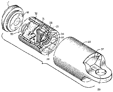
distribution system is shown in Figures 8-12. As ~hown,
this fault indicator 120 includes a generally cylindrical
housing 121 formed of a hard electrically insulating
weather-resistant material such as LEXAN a trademark of
GEneral Electric Company, of Schenectady, New York). The
detector 120 i~ secured to a conventional high voltage cable
122 including an internal conductor 12 by means of a pair of
resilient inwardly-biased non-electrically conductive
retaining arms 123 and 124. The retaining arm6, which
project rearwardly from housing 121, include end portions
123a and 124a, respectively, which are inwardly formed 80 as
to grasp and hold cable 122 in close proximity to the rear
wall 125 (Figure 9) of housing 121. A pair of
semi-resilient stiffening members 126 and 127 may be
provided in close association with members 123 and 124 to
assist in biasing the retaining members against cable 122.
A~ shown to best advantage in Figure 9, upon
insertion of cable 122 between the retaining member~, the
ends of the retaining members are forced apart. This allows
housing 121 to be pushed up against the cable, and as the
- 20 -
7~3
cable abuts the housing the end portions of the retaining
member~ push the cable into engagement. This cable
at~achment arrangemen~ i8 described and claimed in
U.S. Patent No. 4,794,329, issued December 27, 1988 to
S Edmund O. Schweitzer, Jr.
To provide an indication of ~ault occurrence,
de~ector 120 includes on the front wall 128 of housing 121 a
10 pair of windows 130 ~hrough which an indicator flag assembly
131 provides a visible indication of the occurrenct of a
fault current. A handling loop 132 having ends anchored in
the front wall ex~end~ from hou~ing 121 to receive the
hooked end of a lineman'~ tool to facilitate installation
and removal of ~he indicator rom cable 122.
The various circuit components of the fault
indicator are mounted on a circuit board 133 contained
within housing 121. A ~ir~t electrostatic pick-up point
between the detector circuitry and the electric field
surrounding conductor 122 i8 provided by a flat electrically
conductive plate 134 positioned within housing 121 near rear
wall 125 and electrically connected to the circuitry by a
collductor 135~ A second electrostatic pick-up point
radially displaced from the first pick-up point relative to
conductor 12, i~ provided by an electrically conductive
steel ring 139 on the opposite inside surface of housing 121
adjacent and behind front wall 128. This hou~ing
- 21 -
~ 7~
construction, which advantageously provides ~u~icient
excitation to the indicator circuitry without the use of
external ground plane elements, is described in detail in
the aforementioned u.s. Patent No. 4,794,329
S of the present inventor.
Referring to Figure 127 the circuitry of fault
indicator 120 is ~een to comprice a first rectifier network
comprising a pair of rectifier diodes 140 and 141 connected
to the capacitive pickup plate 134 through conductor 135. A
second rectifier network comprising a pair of rectifier
diodes 142 and 143 are connected through a conductor 144 to
the electrically conductive coating 139 providing capacitive
coupling to ground. Together, the two rectifier networks
provide rectification of the alternating current derived
from the electric field surrounding conductor 12 to provide
energization of the trip, reset and trip inhibit circuits of
fault indicator 120.
The pulsating direct current developed by diodes
140 and 141 during normal current flow in conductor 12 i8
applied to a trip capacitor 145 and a trip inhibit capacitor
146 connected across the output terminals of the network. A
zener diode 147 limits the voltage developed across trip
capacitor 145 to the threshold voltage of the zener diode,
and a forward-biased diode 148 connected across capacitor
146 limi~s the voltage across that device during the charge
cycle to the forward drop of th~ diode, typically in the
order of 0.7 volts.
- 22 -
~ 7 ~ 3
The pulsating direct current developed by diodes
142 and 143 is applied to a reset capacitor 150 connected
across the output o~ the second rectifier network to cause
that capacitor to also be charged during normal current
flow.
To provide for periodic reset of the fault
indicator, capacitor 150 i8 periodically discharged through
the series-connected windings 151 of flag indicator assembly
131. To this end, a silicon controlled rectifier 152 i6
periodically conditioned into conduction by the discharge of
a neon lamp 153 included with a resistor 154 in the gate
circuit of the SCR upon the voltage across capacitor 150
exceeding a predetermined threshold level. The neon lamp,
because of its relatively high threshold voltage, typically
in the order of 60 volts, i6 particularly attractive as a
threshold device. However, it will be appreciated that
other devices having appropriate threshold levels~ such as
one or more avalanche devices, could be used instead.
Following the discharge of reset capacitor 150
through windings 151, the voltage across the capacitor
drops, neon lamp 153 extinguishes, and SCR 152 ceases to
conduct~ Capacitor 1~0 then begins to recharge until the
voltage across reset capacitor 150 again reaches the
threshold level of neon lamp 153 and conduction through SCR
152 accomplishes another reset cycle.
Upon occurrence of a fault current in conductor
12, trip capacitor 145 is caused to discharqe in a rever~e
direction through windings 151 of fl~g indicator assembl~
131 through a second silicon controlled rectifier 155~ This
results from closure of reed switch contacts 156 Po~itioned
in close magnetic proximity to cable 122 and connected to
the control electrode of SCR 155 throuqh a gate circuit
comprising a series resistor 157 and a resistor 158 to
ground.
Trip capacitor 145 continues to discharge until
the discharge current is no lonqer sufficient to maintain
conduction through SCR 155 Magnetic pole piece 159 of flag
indicator assembly 131 however remains biased in a magnetic
polarity which maintains the indicator flaq 160 thereof in a
fault indicating position. rlpon restoration of normal
current in conductor 12, it remains for the reset circuit of
reset capacitor 150 to remagnetize pole piece 159 to
opposlte magnetic polarities so as to reposition flaq
indicator 160 to a reset-indicating position.
To prevent false fault current indications as a
result of inrush current associated with initial powerup of
conductor 12, the fault indicator includes, in accordance
with the invention. the trip inhibit capacitor 146 and its
associated circuitry for discharging trip capacitor 145 upon
loss of voltage on the conductor. Tn particular- the
control electrodes of an enhanced FET~type 161 are connected
across trip lnhibit capacitor 146 throuqh a resistor 162
Upon loss of excitation trip capacitor 145 i8 caused to
partially discharge through a resistor 163 into capacitor
- 24 -
~6~;76~3
146. causing the voltage acro~s that device to reverse
polarity and ProqressivelY increa~e in the reverse direction
as the device is charged. Eventually the threshold voltage
of transi6tor 161 is reached and the transi~tor is rendered
conductive by the applied bia from capacitor 146 causing
trip capacitor 145 to rapidly discharge through a resistor
164 and there be unavailable for providing trip current to
windings 151 upon conduction by SCR ~55. Thus~ the fault
indicator is initially non-responsive to fault current
occurring following the loss of voltage in conductor 12. and
does not become operative for this purpose until capacitor
145 again becomes charged.
The operation of flag indicator assembly 131 is
illustrated in Figures 73-16. ~he indicator- which may be
identical in construction and operation to that described in
U. S. Patent d ,495 .439 of the ~resent inventor. is seen to
include an indicator flaq 165 rotatably mounted on a shaft
166 within housing 121. The indicator flaq includes
indicator segments 165a and 165b on either side of the axis
of rotation which preferably each extend less than ~0
around the axis of rotation~
When aligned as shown in ~igures l~a-13b the flag
segments are masked and are not visible to the observer
throuqh windows 130~ ~owever. upon occurrence of a fault
2S current. the indicator flag rotates 90 such that the
indicator segments are Positioned as shown in ~iqures
15a-15b and are visible through windows ~30~ ~he indicator
- 25 -
~ 7 ~ 3
segments are Preferably colored red or another hiqhly
vi~ible color- to clearly indicate the occurrence of a fault
current when viewed through the windows
Actuation of flag member 165 between reset and
fault indicating position~ ifi accompli~hed by an annular
flag actuator magnet 167 which is rotatably coupled to f]ag
member 165 by ~haft 166. ~he shaft is maintained in
alignment with the axis of indicator housing 121 by means o~
a bearing surface in a divider wall 168 (Fiqure ~3- which
n also provides a reset-indicating surface viewable throuqh
windows 70 when the indicator fla~ is in its reset position
This surface is preferably colored white. or some other
color contrasting with the color of the indicator flaq
seqments. to clearly indicate a reset condition when viewed
1~ through the windows-
Actuator maqnet 167. which may be formed of amagnetic material having a high coercive force. such as
cer~aic. is formed to provide four maqnetic poles of
opposite Polari~y. with opposite polarities every 90 about
2n the circumference of the maqnet. ~ctuator maqnet 167. and
hence indicator flag 165- are biased to the position shown
in ~igures 13a and 13b when the fault indicator 120 is in a
non-trip or reset condition by means of a generally
cross-shaped maqnetic Pole piece 170- formed of a maqnetic
2~ material having a relativel~ low coercive force- such as
chrome steel~ ~he pole piece includes four magnetic poles
171-174 in maqnetic communication with flaq actuator maqnet
- 26 -
12 6 ~ / ~ 3
167. ~he Pole piece 170 ie mounted such that the four
magnetic poles extend to Po6itions adiacent the magnetic
pole6 of actuator maqnet 167. ~ magnetic shield 175
(Figures 9 and 10) comprising a flat plate of maqnetically
conductive material is provided between the actuator
assembly and conductor 12 to shield the actuator assembly
from the magnetic field which accompanie~ occurrence of a
fault current in conductor 12.
During normal circuit operation the poles of Pole
piece 170 are biased to the magnetic polarities indicated in
Fiqures 13a and 13b As a result. the opposite Polarity
poles of flag actuator magnet 167 are attracted to position
the indicator flaq 165 as shown. with the indicator ~eqments
thereof vertically aligned and out-of-view of windows 70.
1~ Thus- all that ifi seen is the white reset-indicating surface
of divider 168-
Vpon los~ of voltage in conductor 12. Pole piece
170 is remagnetized to the maynetic polaritie shown in
Fiqures 14a-14b and 15a-15b by momentary energization of
maqnetic windings 151, which are located on the Pole Piece.
as shown. ~s a result, the Poles of flag actuator maqnet
1~7 are repelled by adjacent llke-polarity ~oles of the Pole
piece and the indlcator flag is caused to rotate 90 to the
indicating Position shown in Figure~ 15a-15b Tn this
position- the red indicator ~eqments 165a and 165b of the
indicator flag 765 are visible throuqh windows 70 and a
lineman viewing the fault indicator is advised that a fault
- ~7 -
i70~3
current has occurred in conductor 12.
The indicator fla~ l65 remains in the fault-
indicating Position until the Poles of Pole piece ~ 70 are
subsequently remagnetized to the ma~netic polarity shown in
Fiqures l~a-13b by momentary application of a reset current
to winding& 151 as shown in ~iqures 16a-16b. This causes
flag actuator magnet 167 to again be repelled by the
adjacent poles of pole piece 170 so as to rotate indicator
flag ~65 to a vertical position- as shown in ~iqure~
n 13a-13b
The high input impedance provided by the invention
allows the fault indicator to be utili~ed on test points
where coupling to a monitored conductor may ranqe feom ~ to
only 1 picofarad. and on hiqh voltage cables- where couPlinq
1~ to the conductor may be only 0.5 ~icofarad- without the need
for external qrounding connections or electrically
conductive members projecting from the housing
While Particular embodiments of the lnvention
have been shown and described. it will be obvious to those
2n skilled in the art that changes and modifications may be
made therein without departing from the invention in its
broader aspects. and, therefore. the aim in the appended
claims is to cover all such changes and modifications as
fall within the true spirit and scope of the invention~
- 28 -