Note: Descriptions are shown in the official language in which they were submitted.
2~i67~6
The present invention relates to a radio recei~er which
stably receives a phase modulated receiving signal.
In satellite communication syste~,s~the PSK (Phase Shift
Keying) QAM (Quadrature Amplitude Modulation) system is comparati-
vely often employed from the point of view of transmission effi-
ciency. In the case of demodulati~g the signal modulated by such
modulation system, the carrier is recovered for phase detection,
and assuming n is the number of modulation phases, fO is the car-
rier frequency and fCL is the clock frequency of the digital signal,
the recovered carrier is pulled and stabilized at a frequency
fO -~ m/n fCL and the carrier may sometimes be pulled falsely by
noise. Therefore, it is necessary to control the recovered carrier
so that it is pulled stably to the optimum frequency even when the
line condition results in bad signal to noise ratio.
In order to correct such false pull-in, a sweep track
type phase lock loop (PLL) circuit is known, where when a phase
error signal or a frequency discrimination signal sent from the
demodulator is hiyher than the threshold level, it is judged as a
false pull-in and a sweep signal is applied to a control voltage of
a voltage controlled oscillator for recovering the carrier signal
in order to pull the carrier to the correct frequency, the pull-in
range is equivalently widened by sweeping the recovered carrier
frequency and sweep is stopped under the phase lock condition.
However, :in the demodulator of the prior art utilizing
the sweep track type phase lock loop circuit, if a high level noise
- 1 - '`Y~
is included in an input signal, it is judged as phase asynchroni-
zation and sweep ls started even under the condition that the
recovered carrier is locked to the optimum phase. When the sweep
is started under the phase lock condition as explained above, the
code error characteristic is rather deteriorated.
on the other hand, in recent satellite communication
systems, a highly effective error correcting technique is employed
and it is requested that the system can operate normally even in a
case where the signal to noise ratio of the receiving signal is 0
dB or less. This error correction technique is expected to be
further developed in future and therefore the demodulator is also
requested to operate stably even when the signal to noise ratio is
low.
It is an object of the present invention to realize stable
demodulation by effectively judging start and stop of sweep based on
the decoded code error information in the radio receiver utilizing
a sweep track type phase lock loop,
The present invention controls the recovered carrier by
judging start and stop of sweep of said carrier based on the error
information of the decoded code, for example, the error information
of error correction frequency information, error correction locking
state information in the error correction circult, and quickly
pulls the carrier to the optimum phase and thus realizes stable
demodulation.
253G7-162
In accordance with a broad aspect of tha invention there
is provided a radio receiver which receives a digital phase-
modulated radio signal and outputs a digital signal by
demodulating said received signal, comprising:
demodulatlon means for demodulatiny said received signal
based on a recovered carrier and outputting a phase error signal
as well as a demodulated digital signal;
signal processing means, operatively connected to said
demodulation means, for outputting error information of said
demodulated digital signal;
false lock detection means, operatively connected ko said
signal processing means, for detecting false lock on the basis of
said error information;
sweep signal generating means, operatively connec~ed to said
false lock detection means, for outputting a sweep signal when
said false lock deteation means detects the false lock,
adding means for adding the sweep signal sent from the sweep
slgnal generating means to the phase error siynal sent from said
demodulation means, and
carrier recovery means, operatively connected to said adding
means, for outputting a signal having a fre~uency corresponding to
sald added signal as said recovered carrier.
2a
The invention will no~ be described ln greater detail
with reference to the accompanying drawings, in which:
Figure 1 is a basic functional block diagram of a radio
receiver illustrating the broad principles of the present inven-
tion;
Figure 2 is a functional block diagram of one embodiment
of radio receiver according to the present inventlon;
Figure 3 is a schematic diagram for explaining the recei-
ving signal;
Figure 4 is a functional block diagram of another embodi-
ment oE radio receiver according to the present invention;
Figure 5 is a detailed functional block diagram of a
phase decision circuit used in Figure 4; and
Figure 6 is an operation time chart of the clrcuit of
Figure 5.
Referring to Figure 1, a radio receiver of the present
invention comprises a demodulator 10 which demodulates a received
signal and outputs a phase error signal, a voltage controlled os-
cillator 20 which applies a recovered carrier based on said phase
error signal to such demodulator 10, a sweep signal generator 50
which generates a sweep signal for sweeping the oscillati.on
frequenc~ of such voltage controlled oscillator 20, a signal
processing circuit 30 which corrects the code error oE the demodu-
lated signal and detects such code error and a false-lock detection
circuit 40 which detects when there is a false-lock condition based
on error information obtained by the code error detection function
of such signal processing circuit 3Q, there~y pro~iding a control
~oltage to the voltage controlled oscillator 20 through an adder
60 from the phase error signal sent from the demodulator 10 and
the sweep signal sent from the sweep signal generator 50.
Based on the error detection information by the code
error detecting function of the signal processing circuit 30, the
false-lock detection circuit 40 judges start and stop of sweep and
thereby controls the sweep signal generator 5n. As an example of
error detection information, error correction frequency information
obtained when the siynal processing circuit 30 is used as the code
error correction circuit may be used. Thus, when the recovered
carrier is locked to the optimum phase, the code error of the de-
modulated signal can be reduced even if the signal to noise ratio
is bad and thereby the sweep is not started, thus assuring stable
demodulation,
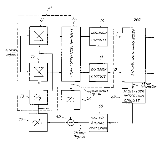
Figure 2 is a block diagram of an embodiment of the
present invention, illustrating demodulation of a 4-level phase
modulated signal. In this figure, the numerals 11, 12 indicate
phase detectors, 20 indicates a ~olta~e controlled oscillator, ].3
indicates a 90 phase shifter, 14 indicates a baseband processing
circuit employing a costas circuit, 70 indicates a loop filter,
60 indicates an adder, 15, 16 indicates decision circuits, 300
indicates an error correction circuit as an example of the signal
processing circuit, 40 indicates a false-lock detection circuit
.~6~
and 50 indicates a sweep signal generator,
The recovered carriers sent from the voltage controlled
oscillator 20 are applied to the phase detectors 11, 12 with a
phase difference of 90 and such phases of the receiving signal are
detected for demodulation. The demodulated signal is then sent to
the baseband processing circult 14, a phase error signal is sent
from the loop filter 70 as the control voltage of voltaye control-
led oscillator 20 through the adder 60 and thereby the phase of
the recovered carrier is controlled, following frequency variation
of the input signal.
The decision circuits 15, 16 decide the levels of the
demodulated signal in the decision timing and apply this slgnal to
the error correction circuit 300, which is provided with a struc-
ture for correcting code error corresponding to the coding format
such as block code or convolutional code of the receiving slgnal
and corrects the code error. Therefore, the error correction
circuit 300 can be said to have a code error detectiny function.
For example, when the block code ls used, since the redundant bit
is added for error correction, it is used for error correction.
Thereby, the error bit is corrected by formation of a syndrome
from the demodulated signal and such error correction frequency is
counted for every constan-t period in order to form error correction
frequency information.
In case such error correction frequency information shows
an abnormally large value, the demodulator can be decided to be in
- 5 -
;7¢~ i~
the out-of-phase condition~ Such decision is made by the false-
lock decision circuit 40. In khis case, the sweep signal genera-
tor 50 is started and the sweep signal is applied to the voltage
controlled oscillator 20 through the adder 60. Thereby, the
frequency of the recovered carrier is swept. In the case where
the error correction frequency informatlon shows a small value,
the demodulator can be decided to be in the in-phase condition.
Therefore, the false-lock detection circuit 40 stops operation of
the sweep signal generator 50 based on the decision thereof.
Accordingly, only the phase error signal is obtained from the adder
60 through the loop filter 70 and the voltage controlled oscillator
20 is controlled, following variation of the frequency of the
receiving signal.
In the case where a convolutional code is used, a Vlterbi
decoder, etc. is used as the error correction circuit 300 (U.S.
Patent No. 4,614,933). If the code error rate is large when a
Viterbi decoder is used, an increase rate Of passmetric also
becomes large and since this passmetric is normalized in order to
prevent overflow of an operational cixcuit, an error detection
information can be formed by counting such normalized signal in
every constant period.
The recovered carrier in such a case where the ~-phase
modulated signal is demodulated has a stable point at every 90
and when it is locked to a stable point other than the optimum
phase point, the demodulated signal must be reversed or inter-
-- 6 --
changed and a phase change circuit is provided for this purpose.
The phase change lnformation for controlling such phase change
circuit is generated on the basis of the code error information.
Therefore, it is also possible to detect code errors and decide
false-lock by making use of such phase change information.
This phase change information can be formed from the
correction frequency information or counting information of norma-
lized signal in the Viterbi decoder as explained before. As shown
in Figure 3(a), a start of message (SOM) signal in the receiving
signal can also be used. Namely, the start of message signal SOM
is extracted from the frame timing signal shown in Figure 3(b) and
false-lock can be decided depending on whether or not the start of
message SOM signal is correctly decoded.
E'igure 4 is a block diagram of the embodiment for making
use of the counting information of the normalized signal in the
Viterbi decoder in decision of false-lock utilizing said phase
change information. In this figure, 10 is a demodulator, 20 is a
voltage controlled oscillator, 30 is a circuit comprising a Viterbi
decoder and a phase change circuit as an example of the signal
processing circuit, 70 is a loop filter, 60 is an adder, 50 is a
sweep signal generator, 31 is phase change circuit, 32 is a Viterbi
decoder, 33 is a phase decision circuit, 41 is a phase change
detector, 42 is a Eorward protection counterr 43 is a backward
protection counter and 44 is a flip-flop. The false-lock detection
circuit ~0 of Figure 2 comprises the phase change detection circuit
7 ~ ~
~1, forward protection eounter ~2, backward proteetion counter 43
and the flip-flop 44
The receiving signal is demodulated in the demodulator
10 by the recovered carrier generated from the voltage controlled
oseillator 20 and thereb~ the demodulated data of I and Q channels
can be obtained, In this case, the phase error signal E is aPplied
as a control voltage of the voltage eontrolled oseillator 20 from
the loop filter 70 through the adder 60 and the freque.ney of the
reeovered earriex generated from the voltage eontrolled oseillator
20 can be eontrolled following frequency variations of receiving
signal.
As explained above, in the ease of 4-phase modulation,
the stable point of reeovered earrier exists at four points every
90 within the phase range of 36Q~ Therefore, when the data of
I and Q ehannels of the sending side are demodulated in the reeei-
ving side, any one of four demodulated data, 1 (I, Q), 2 (Q, I),
3 (Q, I), 4 (I, Q) can be obtained in accordance with the recove-
red carrier phase, Under the conditions of data 2, 3, 4, the
sending signal is not received correctly. Thus is decided by the
phase decision elrcuit 33 and the I, Q ehannels are interchanged
and the data inversed by controlling the phase change cireuit 31.
Thereb~ the demodulated signal under the eondition 1 whieh is
always demodulated by the optimu~ phase is input to -the Viterbi
decoder 32
This phase change cireuit 31 is controlled to chanye the
phase when phase transition of recovered carrier is generated and
~ ~2~6 ~t~t`~
switching is carried out frequentl~ Since the demodulated signal
becomes noisy when the demodulator 10 is locked falsel~, Therefore,
the phase change detection circuit 41 detects a change of control
signal ~hich controls the phase change circuit 31 for switching
and causes the forward protection counter 42 and the backward
protection counter 43 to count the detected signal.
When the content of counting within a certain period is
lowered below the specified value, the forward protection counter
42 applies a reset signal to the reset terminal R of the flip-flop
44, while the backward protection counter 43 applies a set slgnal
to the set terminal S of the flip-flop 44 when the content of
counting within a certain period is increased abo~e the specified
value. An output signal of the Q terminal of this flip-flop 44
becomes the start signal o~ the sweep signal generator 50. In
this case, it is also possible to change the count value of forward
protection counter 42 for outputting the reset signal and the count
value of backward protection counter 43 for outputting the set
signal and in this case the respective count values are set so that
desired forward and backward protection can be realized.
In the case where the phase change circuit 31 is control-
led frequently for changing the phase within a constant period,
since the demodulator 10 is not s~nchronized, the flip-flop 44 is
set by the backward protection counter 43, the sweep signal yenera-
tor 50 is started b~v the set output thereof, and the generated
sweep signal is applied as a control voltaye of the voltage
\
~J~ f ~P~
controlled oscillator 2Q through the adder 60 for sweeping frequen-
cy of the recovered carrier, ~hen the demodulator 10 is phase-
locked, since ~he number of times of control for changing the phase
by the phase change circuit 31 within a constant period is reduced,
the ~lip-flop 44 is reset by the forward protection counter 42,
operation of the sweep signal generator 50 is stopped thereby, and
the ~oltage controlled oscillator 20 is controlled to follow fre-
quency variations of receiving signal,
Figure 5 is a detailed functional block diagram of the
phase dec.ision circuit 33. The phase change circuit 31 and Viterbi
decoder 32 sho~n in Figure 4 are also illustrated here. Circuit 33
includes a phase change circuit 81, a Viterbi decoder 82, counters
83, 85 and 86, a decoder 84, registers 87-90, AND circuits 91-94,
a delay circuit 95 and, a comparison and phase change control
circuit 96.
The demodulated data of I, Q channels are input to the
Viterbi decoder 32 for code error correction through the phase
change circuit 31 and are also input to the Viterbi decoder 82 for
phase decision through the phase change circuit 81. As the counter
83, a quaternary counter is used also for the 4-phase modulated
signal and the combination of demodulated data of I and Q channels
is changed th:rough control by the phase change circuit 81 in every
constant period and any one of the A~D circuits 91 - 94 is selected
by the decodex 84,
The counter 85 counts the lock information sent from the
-- 10 --
7~
Viterbi decoder 46 and applies this information to the registers
87 - 90, the counter 86 decides the counting period of counter 85
and applies its output signal to the counter 85 as the clear signal
and also applies it to the ~ND circuits gl - 94. Such signal
becomes a load s.ignal of the registers 87 - 90 through the AND
circuit selec-ted by the output signal of decoder 84 and a counted
value of counter 85 is set to the register where such load signal
is applied.
The comparison and phase change control circuit 96 com-
pares contents with each other of registers 87 - 90 with a signal
having a constant period which is applied from the counter 86
through the delay circuit 95 and controls the change circuit 31,
upon decision that the phase with the smallest content is a correct
phase.
The lock information described above of the ~iterbi de-
coder 82 is subjected to normalization for prevention overflow of
operational circuit, corresponding to the increment of passmetric
and th.e signal used for such normalization is used as the lock
information. For example, the normalization is carried out by
under the condition that MSB is forced to become "0" when said MSB
of passmetric sent from all ACS circuits (adder, comparator,
selector) becomes "1" and the signal for forcing such MSB to be-
come "0" is used as the lock in:Eormation as explained above.
Since this loc]c information changes frequency of genera-
tion in accordance with a code error rate there:Eore it is counted
-- 11 --
$7~
in every constant period ~y the counter 85~ The demodulated data
of I, Q channels are changed in every constant period in the com-
bination of 1 (I, Q), 2 (Q, I), 3 (Q, I), 4 (~, Q) by the phase
change circuit 81, corresponding to the phase stable point of the
recovered carrier and are then input to the Viterbi decoder 82.
In this case, a combination in such a period ~here a counted value
of the counter 85 becomes smallest indicates the correct phase.
Figure 6 is an operation time chart of the phase decision
circuit, where (a) is an output signal of the counter 86 and CF
represents a counting period. Moreover, (b) is an output signal
of the counter 83. This counter is a quaternary counter and pro-
vides output signals of 0 - 3 through the advancement in every
counting period CF. Signal (c) represents the count content of
count oE the counter 85 and (I, Q), (Q, I), (Q, I), (I, Q) indica-
tes the combinations in every counting period CF of 1 - 4 by the
phase change circuit 81. Signals (d) - (g) indicate contents
of the registers 87 - 90 and the counted values o~ counter 85 are
set thereto as indicated by the arrows~
Signal (h) represents the comparison output o~ th.e regis-
ters 87 - 90 in the comparison and phase change control circuit 96.
Corresponding to the register having the smallest value, the change
control signal (.i) is output and is then applied to the phase
change circuit 31 and phase change detection circuit 41 shown in
Figure 4. The system for eliminating uncertain phase by comparing
contents of registers 87 - 90 is called a comparison and decision
- 12 -
7~6
system.
A code error rate can be obtained by coding again the
data decoded by the Viterbi decoder 32 into the convolutional code
and then obtaining correlation with the input de~odulated data.
Therefore, it is also possible to control the sweep signal gene-
rator with the phase decision circuit on the basis of such code
error rate.
- 13 -