Note: Descriptions are shown in the official language in which they were submitted.
ELECTRONIC POSTAGE MET~R SYSTEM HAVING ARRANGE~ENT FOR
RAPID STORAGE OF CRITICAL POSTAGE ACCOUNTING DATA IN
PLURAL NONVOLATILE MEMORIES
Field of the Invention
$he present invention i~ directed to
nonvolatile memory systems, and more particularly,
nonvolatile memory systems for electronic postage
meters.
Backqround of the Invention
Postage meters are mass produced devices for
printing a defined unit value for governmental or
private carrier delivery of parcels and envelopes. The
te~m postage meter also includes other like devices
which provide unit value printing such as tax stamp
meters. Postage meters include internal accounting
device~ which account for postage value representation
which is stored within the meter. The accounting device
accounts for both the recharging of the meter with
additional postage value and the printing of postage by
the meter printing mechanism. No external independen~
accounting system i5 available ~or accounting for the
postage printed by the meter.
,
; :
:~ ~
I' , s,
.`~'~ :
:
: ' .. ,., :~ , ,~
,: , ,.
r~ f ~ ~I
~ 2 ~
Accordingly, postage meters must possess a high reliability
to avoid the loss of user or governmental funds stored within
the meter and dispensed by printing postageO
El~ctronic postage meters have been developed and are
disclosed, for example, in U.S. Patent No. 3,978,457 for
MICROCOMPUT~IZED ELECTRONIC POSTAGE METER SYSTEM; in U.S.
Patent No. 4,301,507 for ELECTRONIC POSTAGE METER ~AVING PLURAL
COMPUTING SYSTE~S; and, in U.S. Patent No. 4,4841307, for
ELECTRONIC POSTAGE METER ~AVING IMPROVED SECURITY AND FAULT
TOLERANCE FEATURES. Such meters have electronic accounting
circuits which include electronic non-volatile memory
capability for storing postage accounting information. The
accounting circuits and associated postage printing mechanism
are physically sealed within a tamper resistant enclosure.
The non-volatile memories are provided for storing critical
postag~ accounting information when external operating power
is not applied to the meter.
Various types of accounting information may be stored in
the meter non-volatile memory. This information includes, for
example, the total amount of postage remaining in the meter
for subsequent printing (descending register) and the total
amount of postage printed by the meter (ascending register).
Other types of accounting or operating data may also be stored.
For example, service information in the form of error codes
denoting various types of malfunctions or abnormal conditions
encountered during operation of the meter may be stored in
non-volatile memories. This facilitates the evaluation of the
operating experience of each meter to assist in its repair,
should that be necessary, and to accumulate data helpful in
the design of electronic postage meters.
Non-volatile memories as well as the other electronic
accounting circuitry within electronic postage meter are
susceptible to disturbances which can either destroy
information or cause erroneous information to be generated.
The electronic circuits are susceptible to electromagnetic
radiation and electrical transients which can interfere with
the proper operation of the meter and accurate storage of
information. These types of effects can result in a loss of
. .
: - -
:
- . ,;: ,~.:
:
~'
. .
7Z~
funds to the u~ers and, accordingly, it has been
recognized that various types of protection must be
provided to avoid such undesirable results as the data
cannot be reconstructed in mvst instances from other
externally available records.
Electronic postage meters of the type that
write to nonvolatile memories only during power down
sequence such as disclosed in above identified U.S.
Patents 4,301,507, operates satis~actorily ~or their
intended purposes. ~owever, if a difficulty occurs
during the s~v~ral millisecond when external power is
removed and the capacitance within the system provides
the power to writa, critical accounting in~ormation may
be lost. This information may not be able to be
reconstructed because it is not stored in other
nonvolatile memories.
Systems have also been developsd, such as
disclosed in UOS. patent No. 4,484,307 for ELECTRONI~
POSTAGE METER HAVING IMPROVED SECURITY AND FAULT
TOLERANCE FEATURES, and Canadian Patent No. 1,206,619
for MICROPROCESSOR SYSTEMS FOR ELECTRONIC POSTAGE METERS
which have memories wherein data is written into
nonvolatile memories during each operation of the meter.
Other electronic post ge meter systems, such as
disclosed in Canadian patent application of Wallace
Kirschnex, Easwaran C. N. Nambudiri and Douglas H.
Patterson, Serial No. 488,632 for NONVOLATILE MEMORY
SYSTEM WITH REAL TIME AND POW~R DOWN DATA S'rORAGE
CAPABILITY FOR ~N ELECTRONIC POSTAGE METER, where dual
nonvolatile memories are employed, one wherein data is
written during each operation of the meter and another
wherein data is written only during a power down
sequenceO
Summar~ _f the Invention
It has been discovered that electronic systems
~uch as d~scribed above can be improved by an improved
: .,
- ' ' ':
':'
` , ' ' ': ,:
~t~
- 3a -
circuit and sotware arrangement which may employ plural
memories.
The organization o~ the system i5 æuch that
information is written into two dissimilar memories,
under predatermined operating conditions and in a manner
which enhances the reliability o~ the system.
'~ '
, . , : - . : -
,.
. ~ ,;
. . ... . :: . ~
-.... .
., - .:
.
4 .~
A system for the nonvolatile storage of data in
accordance with the present invention includes a
microcomputer means coupled to the data terminals of first
and second nonvolatile memories. The first nonvolatile
memory is of a type requiring data to be applied to its
data terminals for more than a predetermined time for data
to be written into the memory. The second nonvolatile
memory is of a type wherein data applied to the memory data
terminals for less than the predetermined time is
sufficient for data to be written into the second memory.
A program store is coupled to the microcomputer means for
controlling the operation of the microcomputer means to
apply, for at least the predetermined period of time, data
to the first nonvolatile memory data terminals and during
the predetermined time while data is being applied to the
first nonvolatile memory data terminals to apply data to
the second nonvolatile memory means data terminals.
In accordance with a feature of the present invention
the system further includes a power supply coupled to the
~o microcomputer means for energizing the microcomputer means
and energy storage means coupled to the microcomputer means
for energizing the microcomputer means for a time greater
than a predetermined period of time when energization of
the microcomputer means by the power supply means is
interrupted. The program store means controls the
microcomputer to write data into the second nonvolatile
memory when the microcomputer means is energized by the
power supply means and to write data into both the first
and second nonvolatile memory means when the microcomputer
means is energized by the energy storage means.
Other aspects of this invention are as follows:
A system for nonvolatile storage of data, comprising:
a microcomputer means;
a first nonvolatiIe memory having data terminals con-
nected to said microcomputer means for having data writtaninto said first nonvolatile memory by said microcomputer
means, said first nonvolatile memory requiring data to be
applied to said first nonvolatile memory data terminals for
:-
, .
: . ,
~::
7~
a predetermined time for data to be written into said firstnonvolatile memory;
a second nonvolatile memory having data ter~inals con-
nected to said microcomputer means for having data written
into said second nonvolatile memory, said second
nonvolatile memory of a type wherein data applied to said
second nonvolatile memory data terminals for less than said
predetermined time is a sufficient time for data to be
written into said second nonvolatile memory; and
program store means electrically coupled to said micro- -
computer means for controlling the operation of said micro-
computer means to apply, for ak least said predetermined
time, data to said first nonvolatile memory data terminals
for writing data into said first nonvolatile memory and
while data is being written thereinto during said at least
said predetermined time to apply data to said second non-
volatile memory data terminals but not to write data into
said second nonvolatile memory.
A postage meter systam of the type ha~ing a
microcomputer means with first and second nonvolatile
memory means electrically coupled thereto for the storage
of postage meter accounting data, comprising:
said ~irst nonvolatile memory means having data ter-
minals connected to said microcomputer means for having
data written into said nonvolatile memory by said micro-
computer means, said first nonvolatile memory means
requiring data to be applied to said first nonvolatile
memory means data terminals for a predetermined time for
data to be written into said nonvolatile memory means;
said second nonvolatile memory means having data ter-
minals connected to said microcomputer means ~or having
data written into said second nonvolatile memory means,
said second nonvolatile memory means of a type wherein data
applied to said second nonvolatilP memory means data ter-
minals for less than said predetermined time is a
:
: :.
; .
:~:
..
. . . . .
-:
~: I .. :. ~ :. :
2 ~
5a
sufficient time for data to be written into said second
nonvolatile memory means; and,
a program store means electrically coupled to said
microcomputer means for controlling the operation of said
microcomputer means to apply, for at least said predeter-
mined time, postage accounting data to said first non-
volatile memory means data terminals and during said at
least said predetermined time while data is applied to said
first nonvolatile memory means data terminals, to apply
postage meter accounting data to said second nonvolatile
memory means data terminals but not to write data into said
second nonvolatile memoryO
A system for the nonvolatile storage of data comprising:
a microcomputer means;
a first nonvolatile memory having data terminals con-
nected to said microcomputer means for having data written
into said first nonvolatile memory by said microcomputer
means, said first nonvolatile memory requiring data be
applied to said first nonvolatile memory data terminals for
a predetermined time for data to be written into said first
nonvolatile memory;
a second nonvolatile memory having data terminals con-
nected to said microcomp~ter means ~or having data written
: into said second nonvolatile memory, said second non-
volatile memory of a type wherein data applied to said
second nonvolatile memory data terminals for less than said
predetermined time is a sufficient time for data to be
written into said second nonvolatile memory;
program store means electrically coupled to said micro-
computer means for controlling the operation of said micro-
computer means to apply, for at least said predetermined
time, data to said first nonvolatile memory data terminals
~or writing data into said first nonvolatile memory and
during said at least said predetermined time to apply data
~: 35 to said second nonvolatile memory data terminals;
; .~
.. . . .
' ~
- : :
~, :. , .: :
' '
::
~z~
5b
power supply means electrically coupled to said micro-
computer means for energizing said microcomputar means;
energy storage means electrically coupled to said micro-
computer means for energizing said microcomputer means for
a time greater than said predetermined time when energiza-
tion of said microcomputer means by said power supply means
is interrupted; and
said program store means controlling said microcomputer
means to write data only into said second nonvolatile
10 memory means when said microcomputer means is energized by
said power supply means and to apply data to the terminals
of said first and second nonvolatile memories to write data
into both said first and said second nonvolatile memory
means when said microcomputer means is energized by said
energy storage meansO
A postage meter system of the type having a micro-
computer means with first and second non volatile memory
means electrically coupled thereto for the storage of
postage meter accounting data, comprising:
said first nonvolatile memory means having data ter-
minals connected to said microcomputer means for having
data written into said nonvolatile memory by said micro-
computer means, said first nonvolatile memory means
requiring data to be applied to said first nonvolatile
25 memory means data terminals for a predetermined time for
data to be written into said nonvolatile memory means;
said second nonvolatile memory means having data
terminals connected to said microcomputer means for having
data written into said second nonvolatile memory means,
said second nonvolatile memory means of a type wherein data
applied to said second nonvolatile memory means data ter-
minals for less than said predetermined time is a
sufficient time for data to be written into said second
nonvolatile memory means;
a program store means electrically coupled to said
microcomputer means for controlling the operation of said
;~
'.
; ~ . : -
: - . .:
'~ . ' ` . '
.
''~' :,, ,
Z~
5c
microcomputer means to apply, for at least said predeter-
mined time, postage accounting data to said first non-
volatile memory means data terminals and during said at
least said predetermined time while data is applied to said
first nonvolatile memory means data terminals, to apply
postage meter accounting data to said second nonvolatile
memory means data terminals;
power supply means electrically coupled to said micro-
computer means for energizing said microcomputer means;
lo energy storage means electrically coupled to said micro-
computer means for energizing said microcomputer means for
a time greater than said predetermined time when energiza-
tion of said microcomputer means by said power supply means
is interrupted; and
said program store means controlling said microcomputer
means to write data into said second nonvolatile memory
mean~ when said microcomputer means is energized by said
power supply means and to apply data to the terminals of
said nonvolatile memory means to write data into both said
first and second nonvolatile memory means when said micro-
computer means is energized by said energy storage means.
A method for writing to first and second nonvolatlle
memories of a postage meter wherein said first memory is a
type which requiras a longer time for the writing of data
25 thereto than said second nonvolatile memory comprising the
steps of:
(a) writing a byte of data to said first nonvolatile
memory; and
(b) during the wait period while said byte of data is
30 being written to said first memory, writing said data to
said second nonvolatile memory.
A postage meter system of the type having a micro-
computer means with first and second nonvolatile memory
means electrically coupled thereto for the storage of
postage meter accounting data, comprising:
`' -
., - ,,
~,
7~
5d
said first nonvolatila memory me~ns haviny data ter- -
minals connected to said microcomputer means for having
data written into said nonvolatile memory by said micro-
computer means, said first nonvolatile memory means of a
type requiring data to be applied to said first nonvolatile
memory means data terminals for more than a predetermined
time for data to be written into said nonvolatile memory
means;
said second nonvolatile memory means having data ter-
minals connected to said microcomputer means for having
data written into said second nonvolatile memory means,
said second nonvolatile memory means of a type wherein data
applied to said second nonvolatile memory means data ter-
minals for less than said predetermined time is a
sufficient time for data to be written into said second
nonvolatile memory means;
a program store means electrically coupled to said
microcomputer means for controlling the operation of said
microcomputer means to write a byte of data to said first
nonvolatile memory, and, during the wait period while said
byte of data is being written to said first memory, writing
the data in said byte of data to aid second nonvolatile
mamory.
Brie~ Description of Drawings
Figure 1 is a simplified perspective view of a postal
meter showing a simplified diagram of a circuit for the
accounting system of the meter in accordance with the
invention;
Figure 2 is a schematic of the manner in which Figs. 2a-
: 30 2f interconnect to one another for showing the detailed
schematic circuit diagram of the accounting system shown in
Figure:l;
Figure 2a is a detailed schematic diagram showing input
; circuitry for the microprocessor of the accounting system
shown in Figure l;
.` ~
, :
:.
,
: ; .
~':
~671s~
5e
Figure 2b is a detailed schematic diagram showing the
microprocessor and some of the output circuitry, including
an address latch, of the accounting system shown in Figure
l;
5 Figure 2c is a detailed schematic diagram showing
additional output circuitry of the accounting system shown
in Figure 1, including a PROM and a nonvolatile memory;
Figure 2d is a detailed schematic diagram of further
circuitry of the accounting system shown in Figure 1,
including another nonvolatile memory;
Figure 2e is a detailed schematic diagram of still
further circuitry the accounting system shown in Figure 1,
including output circuitry for coupling the microprocessor
of Figure 2b to the printer;
Figure 2f is a detailed schematic diagram uf yet further
circuitry the accounting system shown in Figure 1,
including circuitry for coupling the microprocessor of
Figure 2b to the lift interposer and circuitry for coupling
a minus 30 volt d. c. supply to the microprocessor shown in
Figure 2b;
Figure 3 is a schematic diagram showing the manner in
which the details of flow charts of Figures 3a and 3b are
interconnected to eath other for showing the detailed
: circuitry of the accounting module main line loop;
Figure 3a is a portion of tha flow chart referred to in
Figure 3;
Figure 3b is the remainder of the flow chart shown in
: Figure 3;
~igure 4 i~ a flow chart showing the accounting module
trip processing;
Figure 5 is a flow chart showing the nonvolatile memary
block write routine;
Figure 6 is a flow chart showing the power down
processing routine:
Figure 7 is a schematic diagram showing the manner in
~:
::
. - : :
-: . : .. :~ .
. . .
. . .
,
5f
which the details of the flow charts of Figures 7a and 7b
showing the load normal block data routine;
Figure 7a is a portion of the flow chart showing the
routine of Figure 7;
Figure 7b is tha remainder of the flow chart showing the
routins of Figure 7;
Figure 8 is a flow chart showing the load service block
data from the MNOS or EEPROM memories;
Figure 9 is a flow chart showing computing trip record
10 address routine;
Fig~re 10 is a flow chart showing find current trip
record routine;
Figure 11 is a flow chart showing read first portion of
current primary trip record routine;
Figure 12 is a flow chart showing the trip record
verification routin~;
: Figure 13 is a flow chart showing trip record error
logging routine;
Figure 14 is a flow chart showing set postage on print
20 wheels routine;
Figure 15 is a flow chart showing find current postage
record routine;
Figure 16 is a flow chart showing repair trip record
routine;
Figure 17 is a flow chart showing open nonvolatile
memory block routine; and,
Figure 18 is a flow chart showing update nonvolatile
memory block routine.
Detailed Descriotion of the Preferred Embodiment
30 Circuit Architecture Overview
In the present system both a floating gate EEPROM type
nonvolatile memory and an MNOS type nonvolatile mamory are
: employed in conjunction with a microprocessor having a
-: random access volatile memory. The random access memory,
35 as in the
, .
' ' ' ' ~ ;, ''`''` - `'
~' ~'' '~ ` ' ' . ' .
'.'. `
. '' .;
.
- 6 ~ ,?~,
pre.~ent system, may reside on the integrated circuit chip which
contain~ the microproce~sor. The ~ystem i~ de~igned 50 that
information rom the microproce~sor is both written i~to the
random acces~ memory and into the EEP~OM memory on
transactional basis. The information is written into both the
EEPROM memory and the MNOS nonvolatile memory during a power
down routine. Additionally, writing can occur to both the
EEPRO~ nonvolatile memory and the M~OS memory during block
switching time~, as for example, when the service mode switch
i~ moved from the operating position to the service mode
po~ition .
A unique system of interleaving the writing betwaen the
BEPROM memory and the MNOS memory enable~ the data to be written
into both memorie~ during power down without extending the
perlod of time nece~sary to write into either of the memories
individually. This greatly enhance~ the reliability and
~ecurity of the meter without additionally providing further
ri~k~ that information may be lo~t during power down.
The writing technique i~ such that the writing i3
~ 20 interleaYed. That i9~ a byte of infonmation is first written
: into the B~PROM memory. Since it takes two milliseconds for
the information to be wrltten into the E~PROM memory location~
after the data i~ put on the E~PROM memory data line ports,
this time period i~ u~ed for wrlting two nibbles of data into
: 25 the MNOS memoryO This memory is nibble oriented and the writing
time takes one m~ econd per nibble. Thu~ during the wait
period while the data is baing written into the ~EPROM
nonvol~tilememory the ~ame d~ta 1~ ~imultaneouslybeingwritten
into the MNOS type nonvolatile memory. The interleaving
continue~ until both memories are fully loaded~ith therelevant
: data nece~ary to be stored during a power down sequence.
The above writlng sequence for the particular design
; involved may take approximately 60 to 70 milliseconds ~hile
the power from the capacitanc~ ~tore which is available for
continued operation of the meter after a po~er failure is
detect~d is i~ the range of 200 milli~econd~.
: A~ a further protection because of the neces~ity for the
particular clrcuit di~clo~d to output a 16 bit address at port
2 of the mlcroproce~or, here an 8051 type mlcroprocessvr,
,~
,. .
~,
- 7 ~
when writing to the E~PROM nonvolatlle memory, and since the
MNOS memory is al~o connected to port 2 of the 8051
microprocessor, the addressing scheme fox the EBPROM memory
has be~n selected such that the data lines coupled to the MNOS
memory always are at a high, or one value, whenever the EEPROM
memory is addressed for the purpose of either writing or
reading. This is of a particular importance in protecting the
data in the MNOS memory because of the manner in which writing
must occur in this memory. It should be noted that to write
into the MNOS nonvolatile memory it is necessary to first erase
the 4 bit locations to be written into. To achieve this~ it
is necessary to write ones ~1) into each of the memory locations
and this must be done for a period of time of approximately
10 milliseconds to erase the location and therefore enable a
later write to occur. As a result of this arrangement for the
data input/ ths data lines of the MNOS memory are connected in
a unique manner, specifically, to different pins ~f the same
port as the high order address lines of the EEPROM memory.
With the data lines of the MNOS memory held high for a
period of approxima~ely 2 milliseconds when the EEPROM memory
is being addressed, the MNOS memory is put into a condition
wherein inadvertent writing into memory location is prevented.
This is because should the write enable line inadvertently be
activated during this period of time, the memory locations with
a 1 in them would not change since a 1 is being written in. On
the other hand memory locations with a 0 would also not be
changed because they had not previously been erased and made a
1 to enable the writing step to occur. Additionally, the
erasing process cannot occur because it takes approximately
10 milliseconds to erase a location to enable the memory
location to be written into and the EEPR~M addressing timing
is only 2 milliseconds. t
As a further feature of the present organization it should
be noted that the circuit organization and architec~ure is
such that minimal lines are shared between the EEP~OM
nonvolatile memory and the MNOS nonvolatile memory. This
providesa highdegree of"separation" anda level ofprotection.
Physically, the two memory devices share only 10 I/O lines of
::
.~
.. ; ~
'`"'',
.:
. .
:
~: , ~, -
: .
'. ' `
the microcontroller~ For the MNOS memory, all 10 shared iines
are used only for latching the address. The control lines such
as chip enable, read enable, write enable, and the like, are
totally separated between the two chips. Such separation can
help in reducing any possible mutual interference.
Software ~rchitecture Overview
The software operating the system and the memory mapping
arrangement for storing data,particularly in theEEPROMmemory,
provide a higb degree of redundancy hither to unavailable in
previous electronic postage meters. It has been discovered
that by organizing the real time accounting into two s~ts of
- 20 records in the EEPRO~ memory in a unique manner, additional
reliability can be achieved. Firstly, in the unlikely event
a particular memory compo~ent is unavailable, the software
architecture has been established so that it can function with
either the nonvolatile MNOS nonvolatile memory present or
removed from the syætem. Moreover, the addressing techni~ue
for writing into the EEPROM memory has eliminated the need for
a separate pointer used in previous designs. Specifically,
it has been discovered that data from the piece counter can
be used in the header of the records stored in the EEPROM
memory as a logical record pointer indicating where the record
should be written after a trip has occurred. In the particular
embodiment disclosed, it is the last, least significant 5 bits
~5 of the piece counter which provides the logical pointer for
the record into which the data should be written.
Moreover, it has been discovered by placing the piec~
counting data into the header of each record quick
identification can be ~chieved of the most current record
stored in the EEPROM memory without the necessity, as in
previous systems, of writing header location information twice
per trip, once to indicate new records and once to indicate
old records. Moreover, the techni~ue allows the rapid access
o desired records by a technique which permits a quick search
and identification of desired information. The organization
of the memory is such that there are two sets of twenty records
stored in the EEPROM memory. When the meter is put into
service, the memory locations are initialized so that proper
'
.
' " ! ,
1~ 7,s~,4
g
data l~ stored in all memory location~. ~he use of the piece
count data in the header of each record ~et allow~ a quick
indication of both the oldest and the most ourrent ~previous)
record~ stored. The ~o~t current ~tored record includes the
oldest piece count number which i3 updatad only ater a trip
ha~ been completed.
In the above manner, in conjunction with information
concerning the setting of tha po~tage value in a ring buffer
stored in nonvolatile memory, which data i3 ~tored prior to
the commencement of a trip, should any ~alfunction occur
recon~truction u3ing the ring buffer po~tage settlng data and
the most current tprevious) record allows a recovery from the
fault by using the po~tage v~lue ring buffer ~etting to update
records~ Thi~ avoi~ the nece~ity to pull meters out of
~ervice due to the inabilit~ to recover from a single ~bad
tripN. That i~, a meter operation where data conc2rning the
trip i~ not accurately recorded. A~ an addltion 1 feature in
the me~ory organization, error counter infonmation
maintained for a number of eparate error condition3. Thi~
allow~ enhanced analy~is of failure and fault condition~ which
may occur in the meter wben the me~ory content~ are read and
analyzed.
It ~hould be noted that the two ~ets of twenty records
are de~igned ~o that the primary record ha~ full data. That
~ is the recor~ co~tain~ ~ no~volakile memory write soft error
counter or pointer to remap record; a closing counter ~write
on next trip); a piece counter; a CRC of de~cending regi~ter;
descending register; CRC o~ a~cending register; a cending
regi~ter; CRC o~ dat~ fxo~ the byte 2 to byte 10 hex, thi~
provides a CRC for in~uring that the critical data i correct;
postage value setting batch amounti batch count; PIN number
(for parcel registars only); printer ctatu~ when trip bit i~
cleared, i.e~ thl~ byte i~ written only when the trip iR
completed; and, lastly, a CRC from da a from bytes 2 to byte
lC hex which i~ the CRC of the entire record. In sharp contrast,
; the back up trip record contain~ ahbreviated information of
critical accounting dat~ 3pecifically the in~ormation stored
from byte 2 to bytelO hex mentioned abov Additionally, as
'~ ;'
,
. .
:
: '
a technigue for providing enhanced security a nonvolatile
memory write soft error counter or pointer to a remapped record
is written in the backup record although not at the time of
the transaction or trip. It is an error counter which is
written into only when an error is detected and written into
memory. This is the ~ame case for the main record.
The software functions ~uch that the accounting
microprocessor verifies critical data of both trip ~ecords
stored in the EEPROM and rewrites them if necessary~
1~ Specifically, after a trip is completed the current critical
data resides in three locations in the meter. A first set of
critical data is stored in the microprocessor R~M, a second
full set of critical data is stored in the EEPROM memory and
a third set of abbreviated critical data is stored also in the
EEPROM memory. If upon the comparison (wherein the data in
the RAM is used as the accurate reference data) an error is
detected, a rewrite step occurs. That is, data is rewritten
into the EEPROM memory and thereafter compared to insure it
matches the data stored in the RAM. This is done both for the
full record stored in the EEPROM and the abbreviated data
stored in the EEPROM. It should be noted that the full racord
of the EEPROM memory is not compared; only the critical data
portion of the full record is compared. If, after an error in
the critical data is detected and a rewriting proces~ has
occurred successfully, a soft error counter is incremented to
note the dif~iculty encountered in writing into the EEPROM
memory.
Another major feature of the software is the remapping
of the trip record. Specifically the EEPROM memory is organized ir
such that there are 8 record locations saved in reserve. That
i~ 4 record locations for the main full record and 4 record
locations for the abbreviated record. These locations are
normally not utilized in the operation of the meter. In the
unlikely event a primary record location for either the full
data or the abbreviated data occurs which can be a hardware
failure such as a memory cell failure and the like, the system
is designed to activate an unusad set of record locations.
This is done in conjunction with a pointing techni~ue which
. .
.
.,
~' ' ~ ''' ~' ' '
: .
.~ '
.,:
remaps the primary location to the new activated secondary
location. rrhus~ the reserve secondary location functions in
the capacity of the primary location when this occurs. This
all occurs under software control and this error condition is
noted by the soft error counter for the particular record
location exceeding its maximum, which in the present instance
is 9, or a rewrit~ attempt fails. Thus, a write fails and the
second rewrite att~mpt additionally fails.
The software is further organized to allow an infre~uent
error or transient condition to occur and continue the meter
in service, however, if the transient error occurs more
frequently, the meter is permanently lock out. For example,
if the microprocessor jumps inadvertently for some reason to
an unused or spare location the meter will continue in service
if such does not happen too frequentlyt for example only once
every 10,000 meter trip cycles. Other errors can be treated
in the same manner. This allows segregation of meters which
have a severe but very transient error and those which have a
severe but more frequent Prror which should be removed from
service and corrected by setting a flag in the nonvolatile
memory such that even if the error condition is removed the
meter cannot be initialized by power down and power up.
Additional ~eatures are provided in the software system
to enable an access to descending register stored in the
nonvolatile memory locations from the keyboard and the ability
to dump the contents of the transactional E~PROM memory without
taking the meter out of service by an external device which
communicates with the meter.
Reference is now made to the drawings wherein like
3~ reference numerals designate similar elements in the ~arious
views.
Circuit Operation
Reference is now made to Figure 1. An alternate form of
an accounting control system for a postal meter is disclosed
from that shown in Figure 5 of ~.S. Patent No. 4,301,507 noted
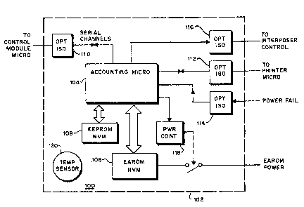
hereinabove. The accounting system 100 includes an enclosure
-~ 102, the walls of which may be formed to provide electromagnetic
~ shielding. The circuits within the enclosure 102 include an
.:.
.,
~.
~ : :
.:
, .. :.. ,,., ": ,
:; ;
- 12 ~ 7/~a~
accounting microcomputer 104 operatively connected to two
nonvolatile memories. The first nonvolatile memory 106 is an
EAROM MNOS type nonvolatile memory. The second nonvolatile
memory 108 is an EEPROM nonvolatile memory. Nonvolatile memory
106 may, for example be an ER3400 manufactured by General
Instruments Corporation, ~icksviller New York and described
in "EAROM" published November 1977 by General Instruments
Corporation and in Bulletin 1203A, "Using the ER3400" published
by General Instruments Corporation. ~he second nonvolatile
memory 108 may be a floating gate electrically erasable
programmable read only memory, as for example, part number
DE5516A manufactured by SEEQ Technology Incorporated, San Jose
California anddescribedin"2816A/5516A TimerE216R Electrical
Erasable ROMs", Preliminary Data Sheet, pu~lished February
1984 by SEEQ Technology Incorporated, San Jose, California.
The accounting microcomputer 104 controls the application
of stored data to the two nonvolatile memories 106 and 108 in
accordance with the present invention. The accounting micro-
computer 104 includes a random access memory which includes
working ascending registers, working descending registers and
the like. The accounting microcomputer 104 also includes a
read only memory control for the necessary routines which will
b~ described in yreater detail hereinafter.
The accounting system 100 incorporates a serial interface,
to enable interfaci~g with the printing and control modules
disclosed in the above noted U.S. Patent No. 4,301,507. The
microcomputer, may for example, comprise an 8051, 8052 or 8751
type series microcomputer from Intel Corporation, Santa Clara,
CaliforniaO In order to avoid damage to the accounting system
100 by electrical surges applied accidentally or intentionally,
and to eliminate electrical noise induced via ground loops,
the accounting microcomputer 104 communicates with the devices
external of the compartment 102 by suitable isolators that are
not capable of applying voltage surges to the microcomputer.
These isolators may, for example, be in the form of opto-
electronic couplers, and are also preferably arranged so as to
be inaccessible from the e~terior of the postal meter. One
isolator unit 110 may be provided for the two way communication
' :
;
, ' ` ' .
' "
. .
:;, ~. :
- 13 - ~ 7 ~d ~ f..~
path with the control unit. A further isolator arrangement
112 may be provided for the two way communication with the
printer unit. A still further isolator 114 may be provided
for applying the power sensing signal to the microcomputer
104~ In addition, an isolator 116 may be provided for
controlling an interposer in the printer for mechanically
blocking functions of the printer.
The purpose of the power control circuit 118 is to provide
power to the system to enable a data transfer operation during
power down operations to be completed when external power
fails. The program of the microcomputing unit 104 is organized
to enter the content~ o~ th~ r~gisters o the micr~computer
and, as appropriate to random access memory, into the
nonvolatile memories 106 and 108 as soon as an indication of
failure of the power supply occurs, and to restore this d~ta
to the workin~ registers upon restoration of power as will be
more fully explained hereinafter.
The enclosure 102 may further include a temperature sensor
120, with suitable circuits, not shown, so that the micro-
computer will ~perate to transfer data to the nonvolatile
memory in the event of excess temperatures by entering a power
failure mode if the temperature is above or below predetermined
limitsr as for example, 70c or 0c, respectively.
The system may prevent the operation of the meter
interposer solenoid, not shown, by way of the isolator 116,
in the event of excessive temperatures. It will be appreciated
that the interposer is controlled by the microcomputer 104
also to inhibit operation of the printer in the event that
insufficient postage remains for a printing operation, or other d`'
accounting data indicates that the meter should not be
operative. ~-
While the isolators have been indicated as individual
units, it i9 ~ of course, apparent that these units may
incorporate multiple devices, so that two way communications
is established in the respective circuits.
Reference is now made to Figure 2. The accounting
microcomputer 104 is connected to the two nonvolatile memories ~-
106 and 108. The address ports oF the EEPROM nonvolatile
.
... ....
- ~ . .
, ~ .
- : -:
~i<.,'~i'7~
- 14
memory 108 are connected to the microcomputer 104 by way
of an addres~ latch 12~. The higher order address ports
A8, A9 and A10 are coupled directly to port 2 of the
microcomputer 104. The data lines of tha nonvolatile
memory 108 are connected directly to the port 1l0ll of the
microcomputer 104 and additionally to an external PROM
124. The PROM 124 can ~erve a~ an extra program memory
capability for the meters accounting circuit or
alternatively as the source of a diagnostic progràm ~or
testing faults or failures of the meter. The MNOS
nonvolatile memory 106 address lines A0 through A7 are
directly connected to the microcomputer 104 port 0. The
higher order address bits A~ and A9 are connected to
port 2 of khe microcomputer 104. The ~our byte data
input/output ports D0 through D3 are directly coupled to
port 2 of the microcomputer.
The nonvolatile memory 106 has two control
lines C0 and Cl which establish the operation to be
per~ormed, namely, read, write, or erase: a write enable
port; and, a chip enable port~ The two ports are
connected to the higher order 2 pins of the port 1 of
the microcomputer 104. The control lines C0 and C1 are
operated from port 1 of the microcomputer 104 by means
of a block erase inhibi~ circuit 12S. The address and
data lines of the nonvolatile memory 106 are connected
to the +5 volt power supply by a series of pull up
resistors 128 and 130 respectively. The pull up
resistors in conjunction with the +5 volt pow r supply
insure that the high level voltage at each port is above
a predetermined level, such as +3 . 6 volts, so that the
hi~h level is above the ~pecified threshold for the
device.
The nonv~latile memory 108 includes three
control terminals, a chip enable ~erminal, a write
ena~le terminal, and an output enable terminal which are
coupled to the microcomputer 104. The chip enable and
write enable line are conne~ted to the microcomputex
~ ,...
- 14a -
through a circuit which includes two negative logic AND
gates 132 and 134. Each oiE these gates will provide a
low output upon the occurrence of two low inputs
' ~
' : :
' ~
~::
:;
. . .
- ~, ' ,.;,, ; ~ '- ,:
:; :. ~.. .
:: ., . . ,, - .
.
. ~ ::-
.
~? ~ ? ~
~ 15 -
at their respect two input terminals~ The devices 132 and 134
operate in conjunction with an NPN transistor 136 to protect
the contents of the nonvolatile memory 108 upon the detection
of the power fail of the operating voltage for the system.
This circuitry operates in conjunction with circuitry within
the nonvola~lle memory to ensure that the nonvolatile memory
108 is in a known condition. When the operating voltage of
the circuit falls below a predetermined level, but is yet above
the level of voltage needed to cause the onboard protection
circuitry of the memory 108 to become active which is 3 volts,
the circuitry including devices 132, 134, and 136 provide
suitable protection for the memory 108.
A negative AND gate 132 is prnvided for manu~acturing
testing purpose~ One of the inputs to the gate 138 is connected
to ground by a resis~or to render the gate 138 essentially
inoperative. When it is coupled to a high voltage, the negative
ANDgate 138 functions to disable the device 124 data lines by
rendering the output enable terminal of the device high.
- A power fail and reset logic circuit 140 is provided.
This circuitry functions to hold the microprocessor 104 in the
reset mode until the voltages have risen sufficiently and
stabilizad. Ad~itionally, on a power down occurrence whe~
power fail is detected, the circuit functions to both insure
that the reset signal is held off until an interrupt routine
is initiated and completed~ Thereafter, the circuit functions
to insure positive application of a reset signal and the
continued application of that signal as the power falls.
A~ power rises; and before the power rises to the level
where it is stabilizedr no current flows through the photodiode
142 of the opto-isolator 144. Thus, the opto-isolator output
photo-transistor 146 is nonconductive. As a result, the output
; of the opto~isolator is maintained at a high level by the i`
ris.ing voltage at the +5 volt ~upply. This results in a
hysteresis buffer 148 pro~iding a high voltage output causing
the NA~D gate 150 to maintain an active signal on the interrupt
terminal of the microcomputer 104. This causes no activity
by the microprocessor because, as will be more explained below,
the microprocessor is being maintained in the reset mode which
: `
,.
7~
- 16 -
overrides the interrupt signal. The high voltage at the output
of the hysteresis buffer 148 is applied via a resistor 152 to
back ~ias a diode 154 coupled to the base electrode of PNP
transistor 156. This causes transistor 156 to be biased out
of conduction which in turn causes NPN transistor 158 to be
biased out of conduction. As a result, the reset terminal
follows the voltage at the ~ voltpower supply andismaintained
active as power rises.
When p~er rises to a sufficient level and stabilizes/
current begins to flow through the photodiode 142 and
phototransistor 14Ç i~ biased into conduction. This causes
the input voltage to the hysteresis buffer 148 to go low and
its output, likewise, to go low. As a result, transistor 156
is biased into conduction causing transistor 158 to also be
biased into conduction. This removes the reset signal from
the microcomputer 104 and simultaneously removes the active
interrupt signal applied by NAND gate 150.
When the phototransistor 146 is rendered nonconductive
due either to a power fail detection signal which causes current
to cease flowing through the photodiode 142 or a failure of
the -30 volts applied causing the supply to rise toward ground,
the interrupt line is rendered active. This occurs because
the hysteresis buffer 148 has a high input applied resulting in
a high output being applied to the NAND gate 150~ As a
conse~uence, a low output signal applied on the interrupt line
and the microcomputer 104 under program control goes into an
interrupt power down routine.
The microcomputer begins to operate under program control
after the operating voltages reach their proper level and
stabilize. The microcomputer continues to operate and e~ecute
main line meter program functions until a power fail occurs
in either the input to the photodiode 142 where current ceases
to flow or by a failure in the -30 volt supply coupled via the
zener diode 160 to the emitter electrode of transistor 146.
Either a failure of the power detect circuit or a rising voltage
on the -30 volt supply causes phototransistor 146 to be biased
out of conduction, biasing diode 154 out of conduction~
Neverthele~s, under program control, an NP~ transistor 1~2 is
.
, .
~ ~,
., .. :
::
:. . :
- 17 ~ 7,~.~
maintained conductive until the necessary power down sequence
has been completed. Thi~ occurs b~ havi~g the emitter electrode
~of the tran~i~tor 162 connected through a resi~tor 164 to
port 33. Tran~i~tor 156 continueq to be maintained
in conduction by connecting the ba~e electrode togroundthrough
the collector emitter current path of tran~i3tor 162 and port
33 of the microcomputer 104. Tran3istor 158 i~ maintained in
conduction until the power down routine is completed and the
voltage at port 33 goes hish biasing tran~i~tor 162 out of
~onduction. When this occurs, tran~i~tor 156 i~ biased out
of conduction. As a re~ult, transi~tor 158 i8 bia~ed out of
conduction and the re~et ~ignal is applied on the reset line.
The microcomputer 104 goes into the re~et mode and remain in
the mode a~ power falls.
A sequence control circuit 1~6 i~ provided for controlling
: the ~equence of application of operating voltage~ to the M~OS
memory 106. The MNOS memory, to properly operate, requires
the ~equenced applic~tion of three separate voltages. This
i~ controlled by the seque~ce control circuit 166. On power up,
a +5 volt operating voltage i8 applied to MNOS terminal 22~
nst ~hown. It ~hould be aoted that the +5 volts i9 applied to
all o~ the various device~ a~ the Vcc and i4 not ~hown on the
~ch~matic circuit diagr~m a~ ~uch. The +5 volt is generated
when the power to the syste~ is turned on. ~hereafter, a -12
volt is applled to MNOS memory 106 pin 2 Vdd. The -12 volts
is applied by ~icrocomputer 1~4 under software control.
Specifically, port 3C goe3 low bia~ng PNP tran~i tor 168 into
conduction. A~ the voltag~ rise-~ on the transi~tor collector
electrode, a ~OS FBT transistor 170 i~ bia~ed into conduction.
As a result the -12 volt~ applied to the ~05 F~T ~ource electrode
: i9 coupled via the device channel to the memory 106 ter~inal 2.
A resistor 172 connect~ th2 terminal 2 to ground to provide a
static di~charge path and protect the device.
When the syst~m i~ turned on, and while the -12 volts i9
being e~tabli~hed at ter~inal 2 of ~emory 106, a MOS fiald FET
transi~tor 174 having its gate electrode connected to micro-
computer port 31, i9 biased into conduction by the +5 volts
pplied via ré~istor 176 to its gate electrodeO ~s a result~
.
.
.
- :.,
~, ...
,:, ~ : ...
:'
- 18 ~ 7
PNP tran~istor 178 i~ biased into conduction and a +5 volt~
is applied to memory 106 terminal 1, Vgg. ThL~ i~ because the
ER3400 device requires the application of a +5 or a -30 volt~
on this particular terminal to avoid an undefined condition
within the device which could adversely affect the memory
operation, ~uch a~ latch up which would prevent acce sin~
memory locations. When the -12 volts has been applied to the
MNOS nonvolatile memory 106 terminal 2, the +5 volt~ i~ removed
from terminal 1 by microcomputer 104 cau~ing port 31 to go
low. The program control of microcomputer 104 will allow port
31 to change fro~ it high cond~tion to its low condition only
after certain routine~ are completed to in~ure that i~
de~ired to effectuate a write operation to MNOS nonvolatile
memory 106 to change a memory location content. When thi~
co~dition occur~; a~ pre~iou~ly noted, port 31 goes low which
bia~e~ MOS F~T transistor 174 out of conduction, causing PNP
tran3i~tor 178 to be bia3ed out of conduction and thereby
removing the application of the +5 volts from the memory
port 31. Simult~neou~ly, a MOS F~T tran~i~tor 180 is bia~ed
out of conductlon which in turn biase~ a PNP transi tor 182
into conduction. When tran3i3tor 182 i~ rendered conductive,
it in turn biase~ a MOS F~T transi~tor 184 into conduction
which results in the appllcation of a -30 volt~ through the
drain ~ource electrode channel to MNOS nonvolatile memory 106
terminal 1. When this ~equence ha3 been completed, the
: microcomputer 104 i~ able to acce~s and write into memory
loca ions within the nonvolatile memory 106.
~ After a write operat~on has been compl~ted, the port 31
: is put in a high ~tate and the FBT MOS 184 i~ bi~sed out of
conduction removing the -30 volt~ ~nd ~he P~P transi~tor 178
i~ bia~ed into conduction applying the +5 volts to the terminal
lo Re~istor~ 186 and 187 in ~onjunction with capacitor 188
coupled to trans$stor 178, and re~istor 190 and capacitor 192
~: coupled to transi~tor 182 function to prov~de a hysteresis
effect. ~he value of the~e component~ are salected such that
both device cannot be operative to 2pply voltage~ to the
terminal at the same time. Thu~, each device goe~ off removing
its respective voltage from te~minal 1 before the other device
turns on to apply i ~ voltage to tenminal 1,
. : .
.
.. . .
, ........ ,.,... "
, ~, '' .
7,~
~ 19 --
Con~unications between the printer microcomputer, control
module microcomputer and interposer are by means of optical
isolators in conjunction with a hysteresis buffer. Thus, the
opto-isolator 116 is coupled by hysteresis buffer 194 to port
12 of r.licrocomputer 104. It should be noted that this is a one
way serial communication channel from ~he microcomputer 104
to the interposer control. The control module communications
to the microcomputer is by way of opto-isolator 110R and
hysteresis buffer 196 to the T0 terminal of microcomputer 104.
Control module communications from microcomputer 104 is by way
of hysteresis buffer 198 and opto-isolator 110T. Finally,
communications from the printer microcomputer is by way of
opto-isolator 112R and hysteresis buffer 200 with communica-
tions from microcomputer 104 to the printer microcomputer by
way of hysteresis buffer 201 connected to port 11 and opto
isolator 112T.
It should be noted that the low order pins of microcomputer
104 port 2 are connected to the high order address pins o~
- . both nonvolatile MNOS memory 106 and EEPROM memory 108. The
higher order pins of port 2 are used as the data ports of
microcomputer 104 for nonvolat.ile memory MNOS 106. When the
EEPROM 108 is accessed for writing or reading purposes, the
microcomputer 104 must output a 16 bit address, the software
selects the address of the EEPROM memory 108 in such a way
that the data input pins of the memvry 106 are at a high level~
Conse~uently, if noise inadv~rtently occurs on the control
lines (write enable, chip enabl.e, C0 and Cl) which would
otherwise condition memory.MNOS 106 to have data written into
it, the memory is still protected against overwriting because
writing a 1 to a 0 in the ER3400 type nonvolatile memory would
not enable an overwriting of the data into a 1. For those
locations where a 1 exists already, the writing has no effect.
Additionally, because of the particular architecture of
the present system, a high degree of isolation exists between
the circuitry employed for reading and writing into each of
the nonvolatile memories 106 and 108. Specifically, only 10
address lines are shared between the two nonvolatile memories
106 and 108. Namely, mlcrocomputer 104 port 0 terminals P00
: . ~. :
'' ' ' .~:
~k3~2
through P07 are shared by devices by memories 106 and 108 as
well as external program memory 124. Additionally, port 2
terminals P20 and 21 (address A~ and 9) are connected to the
high order address pins of the three memory devices 106, 108
and 124. Additionally in port 2, term;nals All, 12, 13, and
14 are connected to the data lines of nonvolatile memory 106.
Finally, port 2 terminal A15 is coupled to control the chip
enable lines of devices 108 and 124.
It should expressly be noted that when program from
external program memory 124 is being utilized to control
operation of the microcomputer 104 the particular systems
configuration provides maximum protection for nonvolatile
memory 106 in a manner similar to that provided when operating
nonvolatile memory 108.
As ~ill be further explained in connection with the
description of the flow charts, the access to the nonvolatile
memories106and108is accomplished by differentmicroprocessor
instructions. The access to the MNOS nonvolatile memory 106
is by input/output mapping techniques. In contrast, a~cess
to the EEPROM nonvolatile memory 108 is by memory mapping
techniques. By utilizing two different accessing techniques
which flows from the particular hardware architecture configu-
ration rather than th~ inherent addressing and accessing
techni~ues of the device themselves, further protection is
provided against inadvertently accessing the wrong memory or
a wrong address while executing rewrite instructions to a
particular memory. Thus, it should be recognized that the two
memories are not each accessed, as for example, by memory
mapping each having different ranges where an inadvertent use
of address in the wrong range could cause access to the wrong
memory. ~gain, both memories are not accessed by input/output
mapping where again a wrong input or output address instruction
could access a wrong memory. This is because memory mapping
access instru~tinns activate microcomputer 104 write lines and
read line (terminals 16 and 17). ~owever these lines are
connected only to EEPROM nonvolatile memory 108 and not to
MNOS memory 106. The I/O map instructions are effectuated by
,,
.
,, , ";
: ,:; . , .
,. . ~: ~ , , .
- ~ ~ :,,,.. :
' . ' ','` :;' '
., : :
- 21 - ~ ~ ~'7~
the high order pins of port l of microcomputer 104 tterminals
5, 6, 7, and 8) which are only connected to the nonvolatile
memory 10~.
Postage Meter Sequence of Operation
Figures 3 through 18 are flow charts representing the
sequence of operation of the postage meter accounting system
100 .
Reference is made to Figure 3, the accounting module main
line loop. The flow chart depicts operation of the accounting
unit 100 after the power up routine has been completed. It
reflects the regular operation of the accounting module. It
should be particularly noted that the operation involve~
receiving and processing the printer status and, in response
thereto writing two trip records to the EEPROM memory 108.
Additionally, when this occurs it sets a trip flag. When the
operation of the microprocessor 104 is caused to loop back to
the main line program loop and continues its processing it
will reach a decision blocX concerning whether the trip flag
has been set. If the trip flag has been set~ it clears the
flag and verifies/rewrite the trip records. Specifically, it
verifies that the trip record was written correctly and if not
correctly written, attempts to rewrite the data into the memory
locationsO It should be noted that the MNOS memory 106 is
written into only during power down (see Figure 18).
Additionally, the MNOS nonvolatile memory 106 is updated during
a switching of the postage meter between its normal and service
mode, should that occur~ -
Reference is now made to Figure 4r the accounting module
trip processing. The flow chart depicts the ma~ner in which
the writing to the EEPROM nonvolatile memory 108 is achieved.
When a postage imprint or dispensation is detected, the
accounting microprocessor 104 performs, under the program
control, the following tasks. It writes the right most two
digits of the unincremented piece count (count of the number
; 35 of pieces processed during an operation o~ the meter) as a
"header" to "close" the pre~ious transaction record. It also
sets the trip flag in the meter status. Additionally, the
microcomputer 104 updates the accounting data in the
~`
. ,
' ~ -,~. '' ~
'` ''" . ~' ~, - '
~. ., :
: : : .:., :: :
- 22 ~
microprocessor RAM and performs a control ~um test. The control
~um i~ the sum of the ascending regi~ter and de~cending regi~ter
of the postage meter which should equal the control sum.
Additionally, the microcomputer 104 wrltes portion of the
current logical tran~action record, which include~ the piece
count, the CRC of the descending register and the descending
register value. A partial CRC for thedatastring i5 accumulated
and stored in a temporary RAM location. The microcomputer 104
under program control seDds the accounting complete message
to the printer module. It further writes the CRC of the
ascending register, the ascending register value and the CRC
of the data string fr~m the piece count to the ascending
register. It goes to receive and process the new ~tatus if
the printer module raise~ the reque~t to ~end signal. The
communications protocol for the various modules i5 described
fully in the above noted U.S~ Patent No. 4,301,507.
The microcomputer 104 wr~tes to the current transaction
record the postage value, batch amount, batch count and PIN
(parcel identlfication number), if it is a parcel register
rather than postage meter. It continues accumulating the data
string CRC.
The program cause~ the microcomputer 104 tc ~ave the last
memory address of the primary full trip record onto the ~tack.
It proceed~ to write the back up (or abbreviated) trip record in
a byte by byte manner so that a reque~t to ~end from the printer
can be served immediately. After writing the back up ~rip
record, the microco~puter 104 waits until the trip bit in the
printer statu3 is cleared, then retrieves, (pops) the memory
addrQ~s of the primary trip record from the stack and writes
the ne~ printer ~tatus and the CRC for the data string of the
entire primary trip record. The ~icrocomputer 104 checkR the
home po3ition chanye and the synchronizatlon between the home
po~ition and the piece count for an error code condition. This
i~ to determine if the ~eter i~ operati~g properly~ The
microcomputer set~ a trip flag which effectively requestslater
trip record veriflcation. It then sends the meter status with
trip completed bit set to the control unit. The trip bit will
be cleared if the outgoing transmi3sion i~ succe~sul. After
this ~5 achieved, the progr~m would return to themainline loop.
.
', ~ .
.
7~rJ.
~ 23 --
It should be noted that the postage value stored in each
primary trip record is used only for reconstructing the postage
fund in case a catastrophic memory failure occurs and the meter
is taken out of service. It is used by the service department
in analyzing the data dumped from a returned meter. During
the power-up loading onto the temporary RAM, the postage value
read from the primary trip record is overwritten by the postage
setting value read from the postage ring buffer which always
contains the current postage setting value. ~hus, if the
setting value is changed after a txip, the current setting
rather than the last trip setting is loaded into microcomputer
random access memory.
Reference is now made to Figure 5, the nonvolatile memory
block write routine~ The routine is called when it is desired
to write into a block of the EEPROM nonvolatile memory 106 and
MNOS nonvolatile memory 108. This occurs only during the power
down o the module or when the meter mode Ls switched from the
normal mode to the service mode by actuation of the service
switch disclosed in U.S. Patent No. 4,301,507. It should be
noted that the program causes the microcomputer 104 to write
one data byte to the EEPROM nonvolatile memory 106 without
waiting. It immediately writes two nibbles or four bits to
the MNOS nonvolatile memory 108 with wait and check, that is,
to read ~ack and verify that the data desired to be written
into the memory locations has in fact been written.
Since a power down interruption can occur at any time, it
is possible that it may be required to write information into
both nonvolatile memories 106 and 108 should a power interrup-
tion occur. To avoid the possibility that a write operation
has occurred within the prior two milliseconds into the EEPROM
nonvolatile memory 106, the nonvolatile memory block write
routine has been arranged such that writing to the EEPR~M
nonvolatile memory 106 does not occur until the processing
loop has operated for at least two milliseconds. Thus, the
first write data to the EEPROM nonvolatile memory 106 occurs
only after the writing of the header to MNOS nonvolatile memory
108. Since this is a two nibble header it takes more than two
milliseconds to accomplish the write cycle.
, ~- ~ ,. .
- 24 -
Reference is nowmade toFigure6,the power down processing
routine. The routine shows the processing of the accounting
unit 100 when a power down situation i~ encounteredO It should
be noted that when the nonvolatile memory blocks are completely
written the routine turns on the connection between the power
fail and reset circuitry to the microcomputer 104 by causing
microcomputer port 33 to go low to operate the circuitry as
previously describedO
Reference is now made to Figure 7, the load normal block
data routine. The routine describes the operation of the
microcomputer 104 to transfer the data stored in the nonvolatile
memories into the microcomputer random access memory. This
occurs during the power up of the accounting unit 100. It
should ~e noted that the source of data for the random access
memory comes from several locations. The data comes from the
normal block data in the MNOS memory 108 it also comes from
the current EEPROM nonvolatile memory 106 normal block data
and lastly, it comes from the current trip xecord data from
the EEPROM nonvolatile memory 106. It should be noted that
the data obtained from these three locations are compared to
make sure that they are consistent. If the data is not
consistent an error message is provided which causes the power
up routine to be aborted. Until the condition is resolved the
meter will not enable and canno, be utilized.
Reference is now made to Figure 8, the load service block
data from MNOS or EEPROM memories. The service block data
contains service and other meter related data needed to operate
the meter such as the high dollar unlock, low postage warning
and other similar types of information The loading of the
service block data operates in a manner similar to the loading
of the normal block data; however, the comparison routines are
not impl~mented due to the fact that this data is not as
critical to meter operation as is the basic normal accounting
information concerning postal funding.
Referenee is now made to Figure 9, the computing trip
record address routine. This routine computes the trip record
address for the ~EP~OM nonvolatile memory 108 so that the
microcomputerl04 will write each trip into the proper location.
, ~
'~
, ,.
'
-
~, .. .
- 25 -
Reference is now made to Figure 10, the find current trip
record routine. This routine provides the abiliky to locate
the current trip record rapidly during the power up process
or responding to a request of the descending register stored
in the EEPROM nonvolatile memory 108. Normally, the current
trip record has the highest piece count value. Instead of
comparing the 8 digit piece count value among the 20 trip
records retained in the nonvolatile memory 108, the routine
compares the ~header" against the least significant two digits
of the piece count for each of the 20 trip records. The trip
record headers were written in real time by the accounting
module trip processing routine previously discussed for Figure
4 For the non-current trip records, the header value is equal
to the piece count value modulo 100. For the current trip
record, the header value i8 different by 20. This is because
the header has not been updated and it still has the piece
count value (modulo 100) of 20 transactions ago. Note that
the current trip record is not ide~tified by a header of a
particular fixed value. In a fixed value header scheme, it
is neces~ary to write the header twice, once when the record
is current and secondly to change it to a different value to
indicate that it is no longer current. ~his would cause the
header locations to wear out before other data area in the
nonvolatile memory with limited write cycle endurance. The
techni~ue described above avoids the difficulty.
Reference is now made to Figure 11, read first portion
of primary trip record routine. The routine is used to insure
that the real time trip record is consistent with th~ normal
block data stored during power up routine.
R~ference is now made to Figure 12, trip record verifica-
tion routine. This routine verifies the accuracy of the
critical portions of the primary and back up trip record. The
critical portions are the piece count ascending and descending
register values. If it is determined upon the verification
that a trip record is bad an attempt is made to rewrite the
data into the same location. If this fails, the record is
rendered inoperative and a new record is written in another
location reserved for such contingencies. ~he loca~ion of the
; ~
..
~'7.'~
- 2~ -
record is remapped to the reserved locations. The remapping
can also occur even iE the rewriting to the original Location
is successful but the number of attempts to achieve the correct---
data write is more than a predetermined number such as nine
attempts.
Reference is now made to Figure 13, trip record error
logging routine. The routine determines whether a remap
operation is necessary and sets a remap flag in the first
nibble of the record to be remapped. It further provides an
indication to where this record will be placed in memory.
Reference is now made to Figure 14, set postage on print
wheels routine. The routine provides a real time writing into
the EEPROM nonvolatile memory 106 of the value to which the
postage meter printing mechanism is set prior to actually
tripping the meter. Speci~ically, the writing into this memory
location occurs prior to enabling the meter for printing, that
is, prior to the time at which the interposer is lifted so
that the shutter bar of the meter printing mechanism can be
operated to allow the printing mechanism to be caused to print.
Thus, even if the power down interrupt routine malfunctions
in some way, data is stored in the nonvolatile memory of the
value to which the print wheels or other printing mechanism
is set prior to commencement of the printing operation and
accounting can be achie~ed on the next power up routine. The
routine provides a protection against multiple failures in the
system which could cause a loss of accounting data.
Reference is now made to Figure 15, find current postage
record routine. The routine controls the microcomputer 104
during power up to find the current postage setting record
last written before the meter became inoperative due for example
to a power failure or to turning off the meter.
Reference is now made to Figure 16r repair trip record
routine. If one cannot locate the current transaction record,
that would indicate that there is some contamination of the
header data and the piece count field. In such an event, the
microprocessor under control of this sub-routine takes the
regular normal power do~n block of piece count data to
reconstruct the last record location for the EEPROM 108 trij
` ;~
~'
. ~ .
' ~ .
-
~
r<~
- 27 -
record. It i5 done in a manner such that all twenty headers of
the transaction records are rewritten to insure integrity of
the repaired trip records. This routine can also be utilized
when the serial number is locked into the meter after
manufacturing and testing to set the piece counter to zero.
Reference is now made to Figure 17, open nonvolatile
memory block routine. The program controls the use of a back
up for emergency service block in the EEP~OM nonvolatile memory
108. It is updated whenever a new MNOS nonvolatile memory
block is open, and it can be uploaded if the regular service
blocks in both nonvolatile memorie~ 108 and 106 are lost or
contaminated~
Reference is now made to Figure 18, update nonvolatile
memory block routine. This routine controls the operation of
the microcomputer 104 when the postage meter is cha~ged between
the normal mode of operation and the service mode of operation.
The routine allows the microcomputer 104 to access only one
of two types of blocks of data, normal accounting information
or service information. The routine insures that both blocks
of information are not simultaneously accessible by the
microcomputer 104. This provides additional protection of the
meter against the inadvertent loss of data and funds.
As can be seen from above the software causes the micro-
computer to operate in a unique manner to achieve an enhanced
reliability. The accounting microcomputer 104 writes two trip
records to the EEPROM nonvolatile memory while the postage is
being dispensed~ Both records contain critical accounting
data including pie~e count, ascending and descending registers,
their CRC's and a data stream CRC. The primary records also
contain less critical data such as postage selection value,
batch count, batch amount, and the like. Accounting data of
~he most recent twenty transactions are always maintained
within the ~PROM nonvolatile memory 108.
The accounting microcomputer 104 verifies critical data
of both trip records and rewrites them if necessary. If the
rewrite is successful, a nonvolatile memory write soft error
counter in the E~PROM nonvolatilP memory 108 for that physical
record is incremented. If the rewrite fails or if the soft
: . :
.. . .
- 2 8 -
error count exceeds a maximum limit, the record will be
redirected to one of the four reserved records~ While a soft
nonvolatile memory error is transparent to an observer, a
redirection to a reserved record would bring the meter to a
~fatal" mode with the new error code 25 and the meter is
immediately disabled. The fatal condition can be removed only
by powering down the meter and powering it up againO On the
next power up; the meter will be locked out if there is no
more reserved record available on either oE the two trip record
sets. At power down or block switching time, the microcomputer
104 writes either operational (normal) or service block data
to both the EEPROM nonvolatile memory 108 and the MNOS non-
volatile memory 106. The microcomputer alsokeeps annemergency
service block" in the EEPROM nonvolatile memory 108. It is
updated whenever a new MNOS nonvolatile memory 108 block is
opened and can be uploaded into the microcomputer random Acce~s
memory if the regular service block in both the M~OS memory
106 and the EEPROM memory 108 are losk or contaminated.
At power up time, the power down block data from both
nonvolatile memories are read into the microcomputer 104 random
access memory. Data in the "trip records" are also searched
and read. If the data are not corrupted and passed the control
sum test, the ascending and descending registers from the trip
record must agree with those read from the power down block
(of the MNOS nonvolatile memory in regular cases), otherwise
the meter will be locked out to preclude further operation as
a code 27 fatal error.
Finally, in the service mode, the descending register of
the current trip record stored in the EEPROM nonvolatile memory
108 can be displayed by depressing the postage meter batch
count key, not shown.
While thi~ invention has been disclosed and described
with reference to the particular embodiments shown herein, it
will be apparent that variations and modifications may be made,
and it is intended in the following claims to cover such
variations and modifications as fall within the true spirit
and scope of the invention.
:
~: .. ,-
: , . .
,
;