Note: Descriptions are shown in the official language in which they were submitted.
3~3
BACKGROUND
The present in~ention relates to a~ apparatus
for recognizin~ a logical status change in one or m~re
channels of an n-bit mu~ tipl ex ~$gnal, especially in
connection with pulse code modulation (PCM) and digital
~ignaling (DS~ devices.
As descrlbed in "P~lichtenheft fur Fehler und
Storungssignalisierung fur PCM- und DS-Gerate" of the
Garman Federal Mails, Central Telecommunications
Offlce, Report N12, FTZ 153 Pfl..., Second Edition,
~everal important functions of a system are monitored
with the assistance of special monitoring clrcuits
incorp~rated n the system devices. When such a
monit~rin~ circuit indicates an error or other
condition, then an indicator in the form of a ~ED is
lit in the device recognlzing the error, and ~n error
report is transmitted. Generally, error reports of a
plurality o devlces are grouped together, and the
error reports of such devices are connected onto common
lines.
The levels of ~igniicance of an ~rror alarm
ts dis~ingutshe~ on the basis o~ priority, or the
urgency ~f the error type. An A type error or urgent
alarm, must be lmmediately handled, even outside o~
regular w~rking hour~, for example during ~ights and
holldays.~ A B type or non-urgent alarm can be handled
during regular w~rk$ng houss. At the lndividual
devlces, the error reports ar2 ~witched on to different
signal llne~ by means o switching bridges. ~s long as
the error conditlon remains, the LED is lit in the
~2-
~L~6'7~3~1
device, and a grounded potential is applled to thesignal line AZ (for type A-alarms) or BZ (for type B-
~larms). The begining of the error condition is also
reported by s2nding a pulse onto a signal line A or B,
whieh results in the excitation of an alarm lamp A or
B. The alarm condition is also forwarded via alarm
lines to another indica$or device and an al~rm lamp A
or B is also illuminated there.
The alarm r0port can be disconnected by
manually pressing an acknowledgment key. This causes a
reminder alarm lamp EL in the signal field, and in the
llght dlsplay means, to be lit, instead ~f the alarm
lamps ~ or B. The reminder ~larm lamp EL can also
light up when a switch or plug in the device is not in
its operakional condition.
The alarm outputs A and B, and the reminder
lamps EL, of a g~ven group of error reports and the
alarm outputs o~ all light display means are combined
to form a ingle collective error signal. This
collectivs error ~ignal is then forwarded to a central
place of opesational supervision, and signifies only
that some ystem part in an operatlng location has
produced an error report. The reminder lamp in the
signal fleld and the l~ght display means arP
illumlnated as long as an error report is being
produeed from a device, ~o ~hat one of the statu~ line~
AZ or BZ remains yr~unded as long as the error report
continues. In addltion, as long as the switch or plug
is not ln its operational cond~tion the reminder lamp
EL also remains energized.
--3--
~L26~723~
20365-2611
In multiplex devices, it i~ desirable that each input
be able to produce a new error report independently of the other
inputs for an error report, for example, the di~connection of an
normal input signal, even when there is already an error report
of an input which has been acknowledged. That is, a pulse must
be produced on the bus line A or B whenever anothar error
occur~, even wh~n the status line (AZ or BZ) is still activated.
In a previously proposed system, an input of an OR
gate i~ provided for connection to receive error reports from
each channel, and the output of this OR gate is directly
connected to the signal line AZ or BZ, and through a pulse
~haper to the signal line A or B. While this results in a
reporting of the first error to occur, subsequent errors are
hidden by the operated condition of the OR gate.
BRIEF DESCRIPTION OF THE INVENTION
.
A principle object of the present invention is to
provide a simple arrangement for the recognition of a lo~ical
status change either from a low value to a high value, or vice
ver~a, in a channel of an n-bit multiplex signal~
According to the invention there is provided apparatus
for recognizing a logical status change in a channel of an
n-channel multiplex signal comprising in combination, an n-bit
~hift register, means for connecting the data input of ~aid
shift register to an n-channel multiplex signal, means for
connecting a source of clock pulses to the clock input of said
- 4 -
7~
,`.D
: . '~
~ . . ' . .
,
:
`' ~
i7~3~
20365-2611
~hift register an AND gate having a first input connected
directly to said multiplex signal and a second input connected
to an output of said shift regi~ter, an inverter connected in
series with one of the inputs of said AND gate, and a D-type
flip-flop having its data input connected to the output of ~aid
AND gate and its clock input connected to ~aid source of clock
pulse~ for producing a multiplex output ~ignal corresponding to
a logical level change in any channel of ~aid n-channel
multiple~ ~ignal.
An indication of a status change from low to high, or
alternatively from high to low, is thereby produced by the
system independently of the status of all other bit~ in the
multiplex signal.
The present invention is advantageou~ly employed in
error signaling for PCM and DS devices, as well as digital
signal channel distributors, because the necessary functions in
connection with error reports can be achieved in a simple and
effective way.
~RIEF DESCRIPTION OF THE DRAWINGS
Reference will now be made to the accompanying
drawings in which:
Figure 1 is a functional block diagram of an
arrangement for the recognizing a logical statu~ change from
a low value to a high value in a channel of an n-bit multiplex
signal;
Figure 2 is a functional block diagram of an arrangement
for the racognizing a logical status change from a high value to a
low value in a channel of an n-bit multiplex ~ignal;
r~
5 -
. ~
~ ,, '~ '
3~3
Fig. 3 ts a unctional block diagram of a
monitoring ciruit of a digital siynal channel
distributor incorporating the present invention;
Fig. 4 is a schematic circuit diagram of time
evaluating apparatus included in Fig. 3;
Flg. 5 is a schematic circuit diagram of logic
means lncorporated in Fig. 3; and
~ ig. 6 is a schematic circuit diagram of a
portion of the apparatus of Fig. 3.
DESCRIPTION OF THE PREFERRED_EMBODIMENTS
Fig. 1 ~hows an apparatus for recognizing the
logical status change from a low value to a high value
in a channel of an n-bit multipIex signal. The
multiplex signal is appli~d to an input 1, and is
connected to the data input~of an n-bit shift re~ister
2, which receives bit clock pulses from the clock
8~ gnal yenerator connected to a terminal 3. An
inverter 4a:is connected to an output of the shift
reg1ster 2, and an AND gate 5 has its ~wo $nputs
connected directly to the input terminal 1, and to the
output ~f the inverter 4a. The output of the AND gate
5 is connected to the data lnput of a D-type flip-flop
6, the ol~ck input o~ which is connected to the
terminal 3.
T~e n-b~t multiplex signal comprises a serial
tream or frame~ of multiplex time slots, corresponding
to n-channels, whlch ~rames repeat at a periodic rate
so that a given ohann~l ~ s ~ound always at the same bit
location in a frame. ~he length of the shift register
--6--
7~38
2 corresponds t~ the number of channels in each frame,
80 that a ~ignal emitted from the output of the shift
register 2 c~rresp~nds to a bit in the fiame ch~nnel,
during the pre~i~us frame, as the bit currently
arriving at the input terminal 1. Thus, the bits
supplied as inputs to the ~ND gate 5 correspond to bits
of the same channel in two succes~ive frames. When th~
new bit has a logical status of a high value and the
earlier bit has a logical status of a low value, then
the output of the AND gate 5 goes high, which places
the ~igh value at the D-input of the D-type flip-flop
6. The flip-flop 6 produces a high level at t~e output
terminal 7 in synchronlsm with the next clock pulse, to
ndicate translstion of a low value to a high value for
part~cular channel of the multiplex signal. The output
of th~ flip-flop 6 for the following clock period,
corresponding ~to the succeeding channel, i5 low unless
there i8 al50 a transist~on o a low statu~ to a high
tatu~ ocourlng in that succeeding channel in the same
two successive pulse:~rames.
Fig. 2:shows an crran~ement for recognizing a
logical status change from a high to a low value in a
channel of an n-bit multiplex systam. ~he arrangement
of Fig. 2 differ Prom that o~ Fig. 1 only in that the
lnverter 4b in conn~cted in series with the other input
of the AND gate. The circuit of Fig. 2 ~unctions to
produce a high level at the outpu~ of terminQl 7 of the
D-typ~ f~ip-flop 6, ~or one clock period, when the
logical level of the mult~ple~ channel associated with
-7-
~.2~3~3
that clock period changes from high to low during twosuccessive frames.
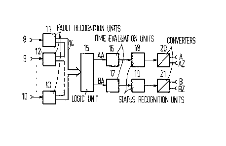
Fig. 3 ~hows a monitoring device incorporating
the present invention. lt lncludes err~r recognition
devices 11-13 which are conventlonal de~ices for
recognizing errors in the operation of various
operational devices connected to their inputs 8-lO.
The units 11-13 are each connected by an alarm bus 14
to a logic unit 15 which is adapted to emit either an
A-type alarm AA or a B-type alarm BA. The A-type alarm
AA is connected to the input of a time-evaluation
device 16 the output of which is connected to the
output of a statu~ change recognition unit 18
constructed in accordance with the present invention.
The output of the rec~gnition device 18 is connected to
the inpu* of a converter 20 which produces an alarm
pulse on a s~gnal 11ne A and a continuous alarm signal
on a~signal line AZ. Corre~pondingly, a B-type alarm
BA is connected to a ~ime-evaluation device 17, the
output of whi~h 1s connected through a status change
racognition unit 19, which produces an output connected
to a converter 21 for emi*ting an alarm pulse on a
signal l~ne B and a ontinuous alarm signal on a signal
line BZ. The error rec~gnltion devlces 11-13 each
correspond, for example, to the commercially available
int2grated module type PE~ 2a30 marketed by the Siemens
Company.
The mon1torlng system of Fig. 3 is capable of
meet~ng ths requirements o~ the German Federal Mails.
The errur and m~l~unction recognit~on dsvices 11-13
--8--
.
723~3
recognize errors at the terminals 8-10 and emit error
reports ln the form of multiple signals to the logic
device 15. ~he err~r slgnals are evaluated there and
forwarded to the time-evaluation devices 16 and 17
alther as urgent alarms AA or as non-urgent alarms BA,
in the form of multiplex signals, so that each channel
of the n-channel multiplex signal may recelve a
separate error ~i~nal. The recognition units lB and 19
develop output signals upon recognlzing a change in
status of the g~ven channel of the multiplex signal,
after a delay of 150 ms through 600 ms, which delay
results from operation of the time-evaluation devices
16 and 17, and the outputs of the recognition units 18
and 19 are forwarded in the ~orm ~f multiplex
signals. The converters 20 and 21 produce pulses (on
signal lines A or 8~ at the begining of an error
condition and continuous signals (on the signal lines
AZ and BZ3, which pulses and signals are recognized at
a central place of operatlons as an error of a given
type associated w1th a unit connected to one of the
specific inputs 8-10.
Fig. 4 shows a schematic circuit diagram of
the logic unit 15 of Fi~. 3. It contains 0~ gates 22
~nd 23, as well as a plurality of swltches 24-27. The
alarm bus 14 has lndividual lines for the various error
condit$ons produced by the recognitlon units 11-13, and
these are connected through the switches 24-27 to an
input of one or the other of the OR gates 22 and 23,
d~pendin~ on whether the givsn line ls associated with
an urgent error or an non-urgent error condition. The
_g_
7~3~3
switche~ 24-27 allow the type of error to be manually
selected for each of the lines of the input bus 14.
The OR gate 22 produces an urgent error signal AA when
any of the lines o$ the bus 14 have an error signal
connected through a switch 24-27 to ~ne of the lnputs
of inputs of this OR gate. Similarly, the OR gate 23
produces an output signal when any 4f its inputs
receive a signal from a line of the bus 14.
The error-indicating ~ignals on the lines of
the bu~ 14 appear at times correspvnding to the time
~lots associated with various channels of an n-channel
(or n-bit) multiplex signal, 80 that only one of the
lines ~f the bus 14 manifests an error condition at any
one time. Alternatively, two or more of the lines of
the bus 14 may be active simultaneously when it is not
necessary to distinguish betwae~ error conditions
occuring in the devices to which such lines are
connected. Thus, the outputs from the OR yates 22 and
23 each oomprise a stream of pulses, correspondin~ to
successive multiplex frames, havin~ bits at positions
corresponding to the active lines of the bus 14.
~ ig. 5 shows details of the time-evaluation
devics 16 ~r 17 of Fig. 3. An input Z8 is connected to
an output of the logio unit 15 to receive either the AA
multiplex signal or the ~B multiplex slgnal. The input
28 is oonnectad t~ the data input of an n-bit
demultiplexer 29 which connects the terminal Z8 to one
of a plurality vf output termlnals, eac~ of which is
conneete to the active-l~w reset ~npu~ of one of a
plurality of counters 30-320 ~he outpu~ of the
--10--
~L~6~;~38
demultiplexer 29 is ~elected by signal on an address
bus connected to the demult~plexer 29 through a
terminal 36. The addre~s bus supplies, repetitively
and sequentially to the demultiplexer 2g, n different
addresss~ corresponding to th~ n outputs of the
demultiplexer so that the multiplex signal supplied to
the tenm~nal 28 ls demultiplexed, with each of the n-
channels being supplied to a separate one of the
counters 30-32. ~he source of bit clock pulses is
applied to a terminal 35 and to the cloc~ input of each
of the counters 30-32. Each of the counters has an
output whlch goes high when the counter has been
counted up to i~s full radix, and each coun~er has a
connaction from its output to an enab~e input, which
operates to disable the counter from further counting,
after it has been counted to its ~ull radix.
When no error report is contalned in the n-bit
multiplex slgnal applied ko the terminal 2~, then all
the counters 30-32 are periodically reset by the low
level output signals ~f the demultiplex~r unlt 29.
:
However, when one or more cha~nels apply to the input
:: ; termlnal 28 ~ontain~ an error s~nal, the reset for a
: ~peci~lc counter fails to appear~ and that c~unter is
then counted to its maximum value. For ~xample, when
~ : an error condition occurs in th~ ~irst channel, no
: ~lgnal is applied to t~e re~et input of the counter 30,
:~ ~o that after e number of bit clock pulses applied to
termlnal 35, corre~pondin~ to tha rad~x of the counter
30, ~he coun~er manlfests a continuous high output
: slyn~l, which per~lsts until ths counter ~s reset by
, , ,
238
the ~bsence of a~ error signal in its channel of the
multiplex signal. This output signal is connected to
an input of a multiplex unit 33, which recelves its
address input over a bus connected to the terminal
36. The multiplexer 33 connects the outputs of each of
the counters 30-32 in turn to the output terminal 34,
so that an n-channel multiplex signal is produced on at
the terminal 34 having channel bits which signal error
conditions in specific channels of the n-channel
ystem, of a duration longer than the counting period
of its respective counter.
Fig. 6 shows a schematic di~gram of the
remaining components of F~g. 3. It incorporates a
status reco~nition unit like that of Fig. 1, with
common components having the same reference numerals.
The n-bit shift raglster 2a is shown in greater detail
in Fi~. 6. The output 7 of the D-type fllp-flop 6 is
connected through a monostable flip-flop 38 and two
diodes 39a and 40a to the base of a transistor 42a.
The base ~s:also connected to a source of low potential
through a resistor 41a, so that the transistor 42a is
normally biased for conduotion. Its collector i~
connected to the:pulse output line A ~for type A
~ignals~ o~ B (for type B signals). The monostable
~lip-flop 38 produces a short pulse in response to the
begining of each output the D-type fllp-flop 6, which
pulse cuts off the ~llp-flop 4~a for a ~hort period of
time, Rnd manlfests a short pulse on the pulse output
line A ~r ~.
~L~67238
The two inputs of the AND gate 5 are connected
respectively to the data input of the shift register
2a, and to the nth output thereof (through the inverter
4a) so ~hat the two inputs of the AND gate correspond
to the same channel of the n-channel multiple~
~ignal.
The n outputs of the shift register 2a are all
conneeted to inputs of an NOR gate 37, the output of
which is ~onnecte~ through two diodes 39b and 40b to
the base of a transistor 42b. The base is also
connected to a low bias potential through a resistor
41b 50 that the transistor 42b is normally blased for
conduction. Its oollector is connected to the
continuous output line AZ (or urgent signals3 or BZ
(for~non-uryent signals). When any of the n-channels
of the n-channel multiplex s$gnal contain an error bit,
~he NOR gate 37 receives an input signal on one of its
several inputs lines at all times, so that a continuous
low ~lgnal is produced at its output, so that the
translstor 42b can maintain its co~duct~ve condition.
When there is no error condition present in the input
multiplex signal, however, the ~utp~t o~ the NOR gata
18 a continuous high ~ignal, whieh maintains the
transistor 42b cut-off. In thic way, the output llnes
AZ and ~Z receive continuous signals in accordance with
whether there is an error or no error in the input
multiplex signal.
It will be apprec~ated by othars sk~lled in
the art that various ~dditions snd modifications may be
made ~n the apparatus of the present invention without
-13-
~67~3~
departing fr~m the essential features of noveltythereof, which are lntended to be def~ned and secured
by the appended cla~msO
.:
;
'" "
-14