Note: Descriptions are shown in the official language in which they were submitted.
This invention relates to elec~rosurgical generators and in
particular to improved circu:Ltry Eor generating RF dri-ve puLse tra:Lns ln
such generators.
With the increase in operating modes of electrosurgical generators
(for example, four CUT and two COAG modes), the need to efficiently generate
these wave shapes both in terms oE cost and parts count is becoming
increasingly important. Typically a substantial number of integrated
circuits and an associated printed circuit card are presently dedicated
to the generation oE RF ON and RF OFF drive pulses. In reducing the cost
of such electrosurgical generators it is important the foregoing circuitry
be substantially reduced.
It is accordingly a primary object of this invention to provide
pulse generating circuits for use in electrosurgical generators which
substantially reduce the complexity and cost thereof.
The foregoing is implemented by using shift registers and other
storage devices such as P~OM's in a novel manner in electrosurgical
generators -to effect the desired pulse generation. Although pulse
~ generators using storage devices of the above type have been employed in
; ~ other applications, their employment in the manner described hereina~ter in
electrosurgical generators is novel.
The invention may be summarized as an electrosurgical generator
comprising a patient circuit including an active electrode and a return
electrode; and means for generating a pulse train in said generator,
characterized in that said pulse train generating means includes at least
one MXN storage device having M memory locations where M > 1 and where
each location contains N storage positions where N ~ 1, said storage device
storing at least one, K-bit blnary signal, where l~CK ~M bits of which are
respective:Ly storecl in the Jth storage positions of K oE the M memory
- 1 ~
.~. ' ,,
:
,;: . ~
~ .
~ t~
locations where J ~; means for sequent:Lally outputting said K-bit binary
signal ~rom said storage devlce; and electrosurgical s:ignal generating means
responsive to the K-bit binary signal Eor generating an electrosurgical
signal and applying this signal to the patient circuit.
The invention will now be described in greater detail with
reference to the accompanying drawings.
- la -
.
.
BRIEF DESCRIP~ION O~ THE DRAWIlilG
Fig. 1 is a partial sehematic, partial bloc~;
diagram of an illustrative electrosurgical generatirlg
system in accordance with the invention.
~ig. 2 is a block diagram of a first embodiment
of an illustrative pulse generator ~or use in the
systern of Fi~ . 1 utilizing a f ixed length shif t regis-
~er in accordance with the invention~
Pig. 3 depicts a plurality of waveforms which
il~ustrate ~he operation of the Fi~. 2 embodimen~
Fig. 4 is a block diagram of a second em~odiment
of an illustrati~e pulse generator for use in the
system of Fig r 1 utilizing variable length shift regis-
ters in accordance with the invention.
Fig. 5 is a block diagram of a third embodiment
of an ilustrative pulse generator for use in the
system of Fig~ 1 utilizin~ a pro~rammable memory in
: accordance wi~h the invention.
. Fig~ 6 depicts data stored in the pr~gramma~le
2~ memory of ~ig. 5 which illustrate the operation of the
embodiment of ~ig. 5.
, . ~ " '' , .., ', ` -
:
Fig. 1 illustrates an electrosurgical generator
~5 10 connected to a patient circuit including an active
electro~e 12 for appl~ing -electrosurgical current to a
patient and a return electrode 14 for returning the
~ current to the generator. The generator includes a
: pulse generator 16 having an RF drive output which
3U con~titutes a pulse train of varying configurations
. . . . . .
., _3_ .
~2~
depending upon the mode of operation of the generator,
The RF drive is applied to a switch 18, which when
closed connects a supply voltage 19 across a tank
circuit 20 comprising a capacitoc 22 and a primary
coil 24, the ~ank being transformer coupled to a coil
26 in the patient circuit. Typically the resonant
frequency of the tank equals the fundamental frequency
of the pulse train applied to switch 18 when the mode
of operatisn is one of the CUT modes while the funda-
mental frequeney of th~ RF drive is typically one-half
that of the resonant frequency of he tank when the
mode of operation is one of the two COAG modes. of
course, the number of modes may vary as well as.th~
frequency relationship between that of the resonant
frequency of the tank and the fundamen~al frequency of
the RF drive,
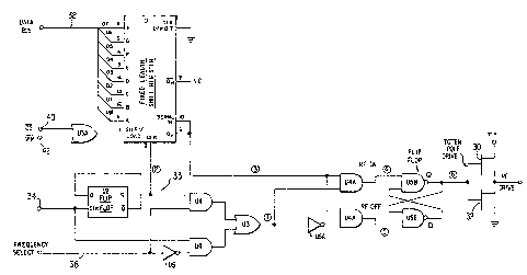
A first illustrative embodiment of the pulse gene-
rator 16 of ~ 1 is shown in Fig. 2 and includes a
fixed length shift register Ulr a flip-flop U2, OR
gates U3 and ~3A, AND gate pairs U4 and U4A, inver~ers
~5 and U5A, a NAND gate flip-flip U~B and a totem pole
drive including FET's 30 and 32. The RF DRIVE output
~how~ in Fig. l corresponds to the ou~put of the totem
pole drive of Fig. 2. It is assumed in the followin~
description of the Fi9. 2 embodiment, the fundamental
frequency of the RF DRIVE pulse train is either 500
kHz or 2S0 kHz. The different wave drives for the
four-CUT waveforms and the two-COAG waveforms consist
of the modulation of these two clock frequencies at a
: 30 multiple of their respective fundamental where a basic
clock signal of 500 k~z is applied to terminal 34.
In order to derive the clock freguencies of 500
k9z or 250 kHz a FREQUENCY SELECT circuit indicated at
33 ls em-loyed. Thi- circuit includes tlip-flop U2
: .. ,, , , . , ~ . ,, :
,
.. ' ~ '' . ...
~2~7~3~3
which is configured as a toggle flip-flop. Its output
Q is one-half the 500 kHz input signal applied thereto
and thus the output of the flip-flop is 250 kHz. The
500 kHz input pulse traln is generated by circuitry
not shown in a known manner. A ~REQUENCY SELECT line
36 is directly cuupled to one of the two parallel AND
gates U4 and through an inverter U5 to the other of
the parallel AND gates U4. The signal on the FREQUENCY
SELECT line is a simple on/off signal which may be
either m'icroprocessor generate~ or hardware generated
in a known manner. The outputs of AND circuits U4 are
connected to an OR circuit U3. Thus, if the FREQUENCY
SELECT line 36 is held high the output of ~3 will be
250 kHz since the output of the flip-flop will be
: 15 gated through the upper AND gate U4 to the OR circuit.
If the line 36 is held low, the output of ~3 will be
~00 kHz since the 500 k~z input signal to the
flip-~lop is also applied to the lower AND gate U4
: where it is ~ated to the OR circuit. The output of ~3
is directly applied to a first one of an A~D gate pair
~4A while thP inverse thereo$ is applied to the second
- AND.gate of the pair via an inverter ~5A. The second
input to the AND gates U4A is the serial output of the
fixed length shift register Ul.
~ 25 The shift register is parallel loaded with an
: 8-bit word, which may be considered an RF mask. It is
loaded when the SHIFT/LOAD line PIN 1 of the register
is held low. This line will be held low when the
inputs to QR circuit U3A are held low. This occurs
when an externally generated CHIP SELECT signal (nega-
tive true), CS, and a WRITE PULSE tagain negative
true~, WR, are applied to the OR gate via terminals 40
and 42. Hence, the OR gate basically performs an AND
function in that both the CHIP SELECT and ~RITE PULSE
5-
signals must be present before the data on data bus
line 38 can be parallel loacled into the shift regis-
ter. The OR gate U3A may be used to effect communica-
tion between a microprocessor and the shift register.
Alternatively, a hardware generated pulse could also
be applied to the SHIFT/LOAD line to load the RF
mask. The fcregoing is true in all embodiments of the
invention. That is, external control si~nals can
either be hardware generated or generated under micro-
processor control.
Once the shi~t register is loaded, the infor-
mation therein may be shifted out serially at a rate
corresponding to the clock rate present at its CLOCK
input line PIN 2. In the present description, the
frequency of the clock is 250 kHz since the Q output
of U2 is connected to PIN 2 of the register and since
it has been assumed a 500 kHz signal is applied to the
toggle flip-flop. The ~5~ kHz clock is suitable for
present electrosurgical generators; however, the fre-
quency of the shift clocked signal could also be selec-
table according to generator requirements. As the RF
mask is shifted out of the shift register at PI~ g
thereof, it is also serially reloaded back into the
register at PIN 10 thereof. Accordingly, the shift re-
2S gister is reloaded wit~ the preloaded ~F mask such
that the mask is continually shifted out and reloaded
- in a bit-by-bit progression. The output of the shift
register is then ANDed with the fundamental clock
frequency at the parallel gates of U4A~ The two clock
signals, RF ON and RF OFF, are generated at the
outputs of these AND circuits where they respectively
set and reset the flip-flop comprising NAND gates U5B.
The Q output of the flip-flop is used as the gate
drive for the totem pole drive arran~ement of FET's 30
`` ; 6
and 32. The common drain point of the F~T's is out-
putted as an on-off pulse train for the RF stage. This
corresponds to the RF DRIVE outpu~ from generator 16
of Fig. 1.
The reset ~ate of the NAND flip-flop U5B will,
in practice, typically have a third input (not shown)
which can be used to shut an RF pulse off before the
R~ pulse is generated. This can be used as a means of
curren~ feedback or over voltage shutdown. That is, if
excessive current is sensed in the output circuit
including tank 20 by sensing means (not shown), the
sensing mean~ will apply a signal to the above mention-
ed third input to effectively decrease the current in
the output circuit in the manner described above. If
other means are employed to compensate for over volt-
age in the output circuit only the R~ ON DRIVE pulses
need be generated where these may be directly applied
~o switch 18 of Fig. 1. In this instance, the NAND
gate flip-flop and the totem pole drive may be elimin-
ated. The foregoing also applies to the remaining
embodiments of the invention.
It should also be noted an edge coupler or dif-
ferentiator tnoS shown) may typically be employed at
the SET input to the flip-flop uSB so that the
flip-flop is set by a short duration pulse. The above
circuit elements have not been shown to simplify the
explanation of the invention.
Typical integrated circuits which may be employed
to implement the circuitry of Fig. 2 are as follows,
it being understood these circuits are but illus-
trative: shift register Ul, a 74LS165; flip-flop ~2, a
74LS74, dual D-type 1ip-flop, U3 and U3A, a 74LS32,
quadruple 2~input positive-OR gates; U4 and U4A, a
74LS08, quadruple 2-input positive-AND gates; and U5,
U5A and U5B~ a 74L~00, ~uadxuple 2-input pOSitiVe-NAND
gates. All of the above circuits are described in the
TTL-Databookl Second Edition by Texas Instruments. The
FET totem pole drive arranyement may comprise a
PNP-NPN eombination of FET's. Information on this com-
bination can be found in tbe databook of the Int~rna-
10 . tional Rectifier Company.
Reference should now be made to Fig. 3 which
depicts variou~ timing wave shapes to illustrate the
operation of the circuitry of ~ig. ~. In particular,
thesP wave shapes result in a twenty-five percent
modulated fundamental frequency of ~00 kHz at a modula-
tion fre~uency of 31.25 kHz. Such an RF drive pulse
train is illustrated as the upper most wave shape in
Fig. 3. Beneath this wave shape is illustrated the RF
mask loacled into the shift register Vl where the
FREQUENCY SELECT line is low - tha~ is, zero. The
encircled num~ers adjacent the remaining waveforms
occur at those points in the Fig. 2 circuit where
similar encircled numbers are indicated. Thus, after
the mask is loaded in the register, the leading edge
of each clock pulse applied to shi~t register ~1
causes the register to be shlfted one sta~e and the
last stage to be outputted at PIN 9. The shape of the
signal occurring at the output o the register is
accordingly as shown at ~ since only the first two
bits of the mask are l's. This output signal from the
register ~requency modulates the 500 kHZ signals
applied to AND gates U4A to provide the RF ON and RF
OFF signals shown at ~ and 0 . These in turn set and
reset the flip-flop to drive the totem pole arrange-
~ . . .
ment so that the RF DRIVE output from the totem pole
follows the gate input at ~ and thus the desired RY
DRIVE pulse train is effected.
Reference should now be made to Fig. 4 which is
directed to a second embodiment of the invention, it
being characterized by variable length shift registers
~2 and U3. The length of the shift registers is
controlled by the binary data set in HEX D flip-flop
Ul. A single gate U~ is used to generate a clock or
1~ latching pulse for flip-flop Ul. The data present on
the data bus at the time of the occurrence of the
write pulse W.R will be latched into the flip-flop if
the CHIP SELECT signal, CS2, is also present. As
soon as the data is l~tched into the flip-flop, the
length of ~he shift registers U2 and ~3 will be set.
The length of the shift registers, whieh ma~ be from 1
to 64 bits, is preferrably equal ~o a multiple of ~he
period of the output RF ON and ~F OFF drive pulse
: trains. These pulse trains are shown at the outputs of
the shift registers and correspond to the RF ON and R~
: OFF pulse trains occurring at the outputs of AND gates
U4A in Fig. 2. Thus, the NAND gate flip-flop U5B and
totem pole drive of Fig. 2 are not shown in Fig. 4 and
in .the subseguent embodiments of this invention al-
. 25 though it is to be understood the RF O~ and RF O~F
.
: pulse trains of the embodiment of Fig. 4 and the other
.
embodiments of this invention could typically be
- applied to a NAND gate flip-flop and totem pole drive
in the same manner as is illustrated in Fig. 2.
The length of the shift registers should be equal
to a multiple of the period of the output RF ON and RF
OFF pulse drive trains. Thus, for a simple on-off-on-
off type repetitive drive, the length would be a
. ,
., ~ , ., ' . .. .
.
.
~;s~
multiple of two~ For a drive with a configuration of
on-off-off-off and then repeating a~ain, the length
would be a multiple of four~ The actual length is thus
determined by how many periods of the output wave
shape are loaded into the shift registers.
The shift registers U2 and U3 are loaded when
their respective CHIP SELECT si~nals, CSl and CS3, are
held low and the data present on the DATA IN line is
~locked in with the clock si~nal CLK where typically
~2 is loaded first and then U3 although, of course,
the order could be reversed or provision could be made
to simultaneously load U2 and U3 in parallel. .The
LOAD/RUN line must also be held high while the shift
registers are loaded from the DATA IN line. Once ~he
registers U2 and U3 are loaded and the period length
is shifted into them, the circuitxy is ready to gene-
rate the R~ ON and RF DRIVE pulse trains. To generate
these trains~ the LOAD/RUN line is held low and the
external clock, - CLK~ is allowed to run. The data
within the shif~ registers is then . shifted out serial-
ly and simultaneously reloaded through input B.
The shift clock frequency is two times the funda-
mental f requency of the RF ON and RF O~ pulse tr~ins .
~he modulation at a lower multiple frequency which was
available in the circuitry of Fig. 2 is also present
in the circuitry of Fig. 4, ~owever, in the circuitry
of Fi~. 4 it is contained within the binary sequence
which is loaded into shift reyisters U2 and U3. ~he
binary sequence reguired to generate the R~ ON signal
of FigO 3 is 10101010000000000000000000000000 and the
RF OFF binary sequence is 0101010100000000D00~00000000
0000. The S~IFT clock freguency is one M~z, this, of
course, being twice the fundamental frequency of 500
- . ~, . . .
`
. . -. ~ .
--1 0--
kH2. The progra~med length of the SHIFT register would
be 32 bits, this corresponding to 2 latched wo~d in
the hex fli~-flop Ul of 010000.
In comparing the first embodiment of Fig. 2 and
the second emb~dim~nt of Fig. 4, it should be noted
that in the first embodiment the fix2d length S~lFT
register is loaded with an ~F mas~ while in the second
emDodiment, the SHI~T registers are loaded with the
actual RF ON and RF O~F signals respectively. It
should also be noted that the embodinlent of ~ig. 2 may
also be employed in a configuration similar to that of
Fig . 4 and vice versa . ~hat is, two f ixed lengths
SHIYT re~isters may be used to respectivel~ generate
the ~ ON and RP OFF signals as is done in Fig. 4. The
1~ RF ON signal would occur at ~) in Fig. 2 and the fYe-
quenc~ select circuit including U2 for selecting the
fundamental fre~uency bf the drive signal would be
eliminated. The shift registers would each be clocked
at a rate twice that of the desired fundamental fre-
:- 2~ quency of the R~ ON an~ RF OFF pulses as is done in
the ~ig. 4 embodiment. If the circuitry of Fig. 4 were
utilized as in the Fig. 2 conf iguration, only one
variable len~th S~IFT register would be used and would
::. be loaded with an R~ mask to ~re~u2ncy ~odulate a
:75 frequ2nc~ selectable cl~ck sîg~al as is dQne in Fig. 2.
'-
' ' ' . - ' ' .
' , ' , -~ ........................ .
O
Although two fixed length registers may be used
in the ~i~. 4 configuration and a single variable
lenyth SHI~T ~egister may be used in the FI~. 2
confîguration, the ~ig. 2 and Fig. 4 embodiments are
.. , - ., -
,
: . , , ' , .
t~
the preferred embodiments for use of the ixed and
variable length shift re~ister embo~iments respective-
ly .
~1 may be a ~C14174, ~lEX D flip-flop; U~ and U3
may be MC14557's, 1 to 64 bit variable length shift
~ registers, and U4 may be an MC14071r ~uad 2-input OR
gate. Details on these circuits are described in
~otorola's CMOS databook or equivalent~ This cir-
cuitry, as stated above, can also be either controlled
b~ hardware o~ ~y a microprocessor.
~eference should now be made to Fi~ 5 wherein an
erasable PR~M is utilized in lieu of the fixed and
variable length shift registers of Figs~ 2 and 4. In
particular, a. counter Ul is used to sequentially
access the memory locations of an erasable P~o~
(EPROM~ U2 where the outputs of the EPROM are select-
able by a multiplexer U3. The gate U4 allows resetting
of the counter either by external means (not shown) or
by a final count decode signal generated by a NAND
gate monitoring circuit U5 which includes a NAND gate
and an inverter.
The EPROM is programmed with the binary formatted
data corresponding to the various RF ON and RF OF~
drives. As will be discussed in more detail below with
respect to ~ig~ 6 r the data ~or a qiven RF ON or RF
OFF driv~ is loaded se~uentially in memory and the
various drives required are loaded in parallel. The
~inary formatted data of Fi~. 6 does not correspond to
the actual binary formatted data typically employed
for the various RF ON and R~ OFF drives~ However, this
data has been chosen for ease of illustration of the
invention. The EPROM extends vertically in Fig. 5;
however, once again for ease of illustration, the EPROM
is extended horizontally in Fi9. 6~ Thus, the EPRO~ is
: . . . .. . . . . . . .
~-12~
8 bits wide and 64 bits long, it being divided into
two banks where BA~K 1 extends from memory locations 0
through 31 while BANK 2 extends from memory locations
32 through 63. In actual practice the EPROM would
typically be 8 bits wide while banks 1 and 2 would
each be 1,024 locations long. An on/off signal applied
to th~ BANK SELECT line selects either BANK 1 or BANK
~. If BANK 1 is selected, 0 is added to the binary
count of counter Ul while if BANK 2 is selected 1,024
is added to the binary count. O$ course~ in the
illustrative example of Fig. 6, 32 would be added to
the binary count if BANK 2 were selected~ In BANK 1,
~ the on and of~ drive pulses for the CUT (Cu), BLEND 1
: IBl~, BLEND 2 (B2~, and ~LEND 3 (B3) signals are
stored in BA~K 1. In particular, the ON wave~orm of
the CUT binary formatted data is stored in the first
bit of the successive memory locations of BANK 1. The
CUT signal is a continu~us sequence of alternating
ones and zeros. Thus, the period of this signal is two
: 20 bits long, twelve periods of this signal are stored in
. .
the first bits of the first twenty-four memory loca-
tions of BANK 1 ~that is, memory locations 0 through
23). The first bits of khe remaining locations 24
: through 31 are not utilized for a reason which will be
described below. The CUT RF OF~ binary formatted data
is stored in the fifth bits of memory locations 0
through 23 of BANX 1. As can be seen this waveform is
the inverse of the cut RF ON waveform. Again, memory
locations 2d~ through 31 are not utilized.
The BLEND 1 RF ON binary data is stored in the
second bits of memory locations 0 through 23. The
illustrative period of this waveform is 8 bits long
and the waveform itself constituting the se~uence
~ . . : . , .
-13-
~ 2~
1010000D. As can be seen in Fig. 6 this sequence is
repeated three times to fill the second bits of memory
locations 0 through 23. The BLEND 1 RF OFF binary data
is stored in the sixth bits of memory locations 0
through 23 and, of course~ three periods of this
waveform are also stored in the first twenty-~our
memory locations. The RLEND 2 and BLEND 3 O~ and OFF
waveforms are respectively stored in the third,
fourth~ seventh and eighth bits of the first twenty-
four locations of BANK 1 where three per;ods of each
of these waveforms is stored. Again, the memory loca-
tions 24 through 31 are not utilized. Hence, none of
the latter locations are utilized in BANK 1.
T~e COAG 1 and COAG 2 ON and OFF RF drive
waveforms are respectively stored in the first, sec-
ond, fifth and sixth bits of the first twenty-four
memory locations of BA~K 2 ~-- that is, memory loca-
tions 32 through 55. Again, the last 8 memory loca-
: tions of the BANK are not utilize~ -- that is, loca-
~ions 56 through 63. Moreo~er, none of the third,
fourth, seventh or eighth bi.ts of any of the memory
locations o~ the second BANR are utilized. Three
periods of the COAG 1 ~or spray COAG) O~ and OFP
waveforms are respectively stored in the first and
; 25 fifth bi~s where one period of the COAG 1 ON waveform
is 11000000 and one period of the OFF ~aveform is
00110000. Two periods of the COAG ON and OFF 2 wave-
forms are respectivel~ stored in the second and sixth
bits as can be seen in Fig. 6. It should be noted that
24 memory locations from each ba~k arê thus utilized
to store all of the CUT and COAG wave~orms, as will be
further discussed below.
In operation, assume it is desired to generate
the BLENDED CUT (B3) ON and OFF RF drive pulses. The
-14-
~26~ ,?~
binary form~tted data Por th~ese pulses is stored in
the ~ourth and eighth bits of BANK 1. Hence, the level
of the sisnal on the BANK SELECT line will be at that
level which will select BANK 1. Moreover, applied to
the A and B inputs of the multiplexer will be a binary
3 -- that is, the DRIVE SELECT 0 and DRIVE SELECT 1
lines will both have high levels or ones applied
thereto, which will cause the multiplexer to select
the outputs from the fo~ ;h and eightb ~its of each
- 10 memory location as that location is accessed by
counter Ul.
Assuming the counter has been reset, it will
begin counting as soon as the CLOCK applied to PIN 10
is allowed to run the count, of course, bèginning from
zero. ~hen the number zero is applied to the PROM, the
zero (or first) memory location will be accessed where-
by the first throu~h eighth bits of the first loc~tion
will be respectively applied to the output PI~S 0
through 7 of the PROM. In particular, the binary
2~ sequence 11110000 will be applied to these QUtpUts
~rom the first BANK. Since the multiplexer has been
set to select the fourth and eighth bits of ea~h
accessed memory location, the bit 1 will be applied to
the ~F ON output line of the multiplexer while the bit
3 will be applied to the RF O~F line. When the counter
steps to 1, the second memory location is accessed to
apply the sequence 00001111 to the multiplexer where
again the fourth and eighth bits are selected to apply
the bits D and 1 as RF ON and OFF outputs respective-
ly. In this manner, the successive binary outputs of
counter Ul are decoded in U2 to effect sequential
accessing of the successive memory locations of the
P~O~ to generate the B3 RF ON and OFF pulse trains.
, ~ , . - , .
-15- .
~lZ~
~7hen the counter reaches the binary value of 23 (that
is, the last memory location where a B3 data bit is
stored~, the conditions or the NAND gate U5 will be
satisfied to generate a reset pulse through ~4 to
reset the counter to its zero value. The counter will
again step through 24 counts to generate thre~ more
periods of the B3 waveform. Thus, the B3 waveform will
be generated as long as the CLOCK is applied to the
counter.
From the foregoing it is clear the counter resets
after 24 memory locations have been accessed. More-
over, as described above, all of the CUT and COAG
waveforms occupy the first twenty-four memory loca~
tions of either BANX 1 or BANK 2. Thus, regardless of
whether a CUT or COAG signal has been selected9 the
same NA~D gate U5 can be employed to effect resetting
of the counter and, of course, recycling of the vari-
ous RF ON and OPF drives. 1`his has been e~fected by
noting that the period of the CVT waveform is two bits
long while the period length of the blended cuts and
the COAG 1 waveforms is 8 bits and the period length
of the COAG 2 waveform is 12 bits. Thus, the lowest
common multiple of the numb~ers 2, 8, and 12 is 24~
~ence, by storing the number of periods of each wave-
form necessary to occupy 24 memory locations, the
simple NAND gate U5 can be employed to reset the
counter at the common count of 24 to thus provide a
simple circuit for generating all of the waveforms.
~s noted above, each of the BANKS is 32 memory
locations long. Since the lowest common multiple of
the period lengths of the different waveforms is 24,
it is not necessary to use the remaining eight loca-
tions of each ~A~K.
~ -16-
. .
From the foregoing it can be seen that the BANK
SELECT si~nal (either high or low) determines whether
the output will be a CUT or COAG signal. The four CUT
signals are selected by the combination of signals
applied to the A and B inputs of the multiplexer U3
where, for example, low signals applied to each of
these inputs would select the CU~ ON and OFF RF
signals, a high signal applied to terminal A and a low
signal applied to terminal B would select the blended
CUT (Bl~ signals, a low signal applied to terminal A
and a high signal to terminal B would select the 32
signals and,- as described in detail above, high sig-
nals applied to the A and B terminals select the B3
signals. The foregoing, of course, assumes the first
BANK has been selected~ If the second BAMR is select-
ed, 32 is added within U2 to the output of counter ~1
to select the second bank and the COAG 1 signals are
selected by applying low signals to the A and B
terminals of the multiplexer while the COAG 2 signals
are selected by applying a hi~h signal to terminal A
and a low signal to terminal B.
As stated above, the binary formatted data employ
ed in Fig. 6 is illustrative. In actu~l practice, the
length of the period of a CUT signal would be tw~ bits
as shown in Fig. 6. However~ the length of the period
of the blended CUT signals is each 48 bits as is the
COAG 1 waveform while the period of the COAG 2 wave-
form is 68 bits. The lowest common multiple of these
. numbers is 816..... Thus NAND gate U5 is set to be
: 30 responsive to that num~er as is illustrated in Fi~. 5
to effect c~clic resetting of the counter.
In summar~, external circuitry selects which BAN~
is to be accessed. The BANK SELECT allows up to ei~ht
: , . ... . :
-17-
3~
pairs o~ RF ON and RY OFF drives to be stored in
memory at one time where in the pres~nt embodiment
only six pairs are stored. Once a BANIC has been
selected and counter ~1 has been reset, the multiplex-
er DRIVE SELECT lines are set to determine which ~ns
of the four drive pairs is to be selected. Then ,he
C~OCK is allo-~2d to run and the counter begins
counting.
The memory locations of the PRO~ are then seguQn-
tiall~,r accessed and the eight-bit wide words at the
: memory locations sequentially appear at the inputs to
the multiplexer. Only those two 5 ignals s~lected by
the DRIVE S~LECT lines are transmitted through the
multiplexer and appear at the ~F ON and RF OFF outpu~
lS terminals. The pulse train generated is therefor the
sequential data bits stored in a given data position
within the EPROM.
The embodiment of Fig. 5 results in a lea~t par~s
.count or a circuit which has a si~nal with frequencies of .
~0 '750 kBz (CUT), 81.25 `~Z tthe blended CUT and ~OAG 1
si~nals), and 22~05 k8z tthe COAG 2 si~nal). The
fundamental frequencies employed in this embod~ment
would be 750 k~æ and 375 Ic~z. Thus the input ~lock
rate to the counter would respectively be 1.5 mH~ and
~5 75~ kHz ~or these ~wo fundamental fre~uencies. A~ the
1.5 mHz clock rate the number of ~iemory loca~ions
reguired for the three above periods are 2, 48, and
- 68. It is possible to have ~he end point of th~
coun'er be selectable for these three lengths however,
the chip count wDuld be high. Thus, in accordance with
the embodiment o~ Fig. 5, one end count is provide~ -
for all o~ the periods and the desired signals are
repeated a number of times for those signals which are
~ . . .. . .. .. . . . . . ....
-18-
~Z~7~ ~
shorter than the end count. Although, as stated above,
an end count of 48 would suffice for the CUT and COAG
1 signals, it would not for the COAG 2 signal, which
requi~es an end count of 68. Thus, the least common
multiple of 816 permits a common end count suitable
for all drives which can be detected by a single chip
U5. Since 816 is less than the 1,024 lengths of BANKS
1 and 2, all requirements are satisfied.
Thus all that is required is to load the PROM
sequentially with the required binary information for
the six RE ON and six RF OFF driYe trains. For the C~T
train, the signal is repeated 4D8 times, the BLE~DED
CUTS AND COAG 17 times, and the COAG 2 train 12 times.
Although some redundancy occurs, the final decode cir-
cuit U5 for 816 becomes a single four input NAND gate
and an inverter~ This, as stated above, resets the
counter to start the counting from zero again when the
final count is reached in a simple and straight~orward
manner.
Typical components which may be employed in the
embodiment of Fig. 5 are as follows where it is again
to be understood these components are illustative and
the invention is no~ limited thereto: Ul may be a
MC}4040, 12-bit binary count~er, U2 may be a 2716, 2KX8
W erasable PROM; ~3 may be a dual 4-channel analog
multiplexer; U4 may be a Mc14071, quad 2-input OR
~-- GATE; and U5 a MC14012 dual 4-input NAND gate.
There are several variations of the third embodi-
ment which are possible, although the embodiment of
Fig. 5 is preferred. ~he PROM can be replaced by a RAM
and a microprocessor can load the device specifically
for the DRIVE train required so that the output multi-
plexer is not required. The same two output data bits
..
'' . ' , . ,., , ,,, ~, . . . .
` , ~19-
~r~ alw~y~ used ~or the ~F 0~ a~d R~ 0~ ~ignals, for
example, the fir~t and fiftb output data terminal~ for
~he CUT signals. The decode circuitry U5 can al~o be
i~plementad by latching the Pin~l count into a MC
14174~ H~X D type flip-flop, or gguivalent ~nd comp~r-
ing the ma~nitude of addre~s coun er Ul to the final
coun~ ~et in the flip-flop~ ~hen the two counts are
equal the coun~er would be r~etO ~ circuit whi~h
compare~ the counts i~ a 74LS85, ~ four bit m~nitu~e
co~par~tor,
Again, as in the last example~ the RF ON and ~F
O~F DRIVE output8 are st~e~d to the ~AND gat~ flip-
flop to set al d re~et it to drive the gates of the ~ET
totem pole to genera~e the actual RF DRIVE signal.
- 1~ It should also be noted that although the outputs
fro~ the various storage devices ha~e been taken ~e-
quentia~lly, they could al80 be t~ken ~n p~ral~el an~
~pplied to a parallel-tv-serial conv~r~t~r or ~he lik~
to develop the desired pulse train~ These and other
~imilar modifi~ations will be apparen~ to those ~kill-
. ed in this ~rt.
~'~ ' , ' ' '. . ' .
. . . ...
~ ~ ' ' . - " ' " ' ' ' . . ' " " ' ' , - '
.
' ' ' ' " ' '' ' ' ' " ' ' ' . ' '' ' .' " ' '. ':, ' ~ .' ' ' . ' . . ' ~:
.,, ~ . . - . . .
.. . . . . . . . . . - . . . .
,' ' '. . ' - ' ' - . ,. ` . -, . ~ . ' '' . ' . . ' , ' .
. . . ~ . .. . . . ..
: