Note: Descriptions are shown in the official language in which they were submitted.
f~ ;i J~L~ ~I
PROGR~MMABLE DATA ~ATH WIDTH IN A PROGRAMMABLE
~ ~S
.. 5 This application is a division of Canadian
application 491,922-0 filed September 30, 1985.
~ the Invention
: Field of the Invention
This in~ention relates to a prograImn~ble unit
having plur~1 levels of subi~s~ruction sets and ~re
particularly to such a unit wherein a portion of the lower
level instruc~ion set is embedded in the upper level
ins~,ruction set.
~1
~z~
-2~
Descri~tion of the Prlor Art
The term "microprogram" was first coined by
Maurice Wilkes in his paper "The Best Way to Desi~n an
Automated Calculating Machine," Report of the Manchester
University Compu~er Inauguxal Conference, Manchester, England,
July 1951, pp 16-18. This paper described a machine
ins~ruction decoder that was, in essence, a diode matrix
which served as a read only memory. The machine language
instxuction was employed ~s an address to this read only
memory and the respective control signals were then read out
from the memory and sent to the various functional units
of the processor to effect the given operation. Such a
machine ins~ruction, sometimes called object code,
involved a sequence o~ steps which reyuired that a number
of the sets of control signals be read out of ~he memo~y in
a sequence to execute the given machine Ianguage instruction.
Each set of control signals became known as a micro
instruction and the machine 1anguage instruction is often
referr~d to as a macro instruction.
It was a number of y~ars, however, before
Professor Wilkes' idea became practical since most
compu~ers required a large number of control signals for
each ~lock period, which meant that the control store, or
micro progxam store, had to contain no~ only a large
number o~ bits in each micro instruction but also had to
contain all o~ the se~uences of micro ins~ructions necessary
to execute all of the respective macro instructions. Howe~er,
core memories or diode memories at that time were too large
and bulky, as well as expensive, to be placed inside of the
processor as an ins~ruction decoder. Furthermore, the
resultant micro instruction fetches from memory were slower
than could be obtained from a hardwired logic decoder.
~l ZiE;, ~. L~
-3-
With the advent of commercially available in~egrated
circuits, processors could not only be reduced in size and
increased in speed but also m~emories became cheaper and aster
and the ~irst micro program computer to be marketed on a wide-
spread commercial marke~ was introduced by IB~ as a seriescalled System/360 (see the Amdahl et al. U.S. Patent No.
3,400,371). Actually, the micro program mem~ries of some
membe~s of that series were formed of capacitor cards.
In System/360, the micro instructions were a
set of control signals which were dividad into groups or
fialds with each group or field being encoded in order
to conserve the number of bits required to be stored in
mlcro memsry. These ~ields were then decoded for simultaneous
execu~ion of the various units of the processor. In
earlier developmental micro programmed processors, thè entire
mlcro i~s~ruction was encoded in order to save memory space
which required ~hat the micro instruction itself had to be
decoded to obtai~ the necessary control signals. The
former type of partially encoded control signals into fields
Zo b~came k~own as hori~ontal micro instructions while the latter
~ype of micro instructions, which were completely encoded,
were called vertical micro instructions. Nevertheless,
with ei~her type of micro inst:ruction, a complete sequence
of such mlcro instructions had to be stored for every
macro instruction that was to be decoded.
In order to reduce the numher of micro instructions
that had to be stored, the concept was developed of two
levels of control stores where the lower level was required
to contain only each unique micro instruction rather ~han
sequences of micro instructions which were redundant. A
smaller memory in terms of word or instruction widths was
supplied to contain a sequence of encoded micro instructions
which served as addresses to corresponding horizontal
;~2~
_ -4
mlcro instructions written in the lower level store. Such
a system is described in tha Faher et al. U. S. Patent
3,983,539. In such a system, the lower level control store
could be a read only memory, which is cheaper than a random
access memory, while the upper level memory would be a
random access memory. To distinguish between the shorter
vertical m1cro in~tructions in the upper level memory and
the longer horizontal micro instructions in the lower
level memo~y, the upper level memory was called the
mic~o ~emory and ~he inventors of the Faber patent called
the iower level memory a nano memory and the horizontal
micro instructions were called nano instructions.
First embodiments of this plural level
- subin~truction set processor required several hundred
integrated circuit chips for implementation since at that
time such integrated circuit chips contained only a
handfull of logic gates per chi.p. As integrated circuits
were d~veloped with greater packing densities, i.e., more
gates psr chip, fewer chips were req~ired to build the
processor. The earlier chips were referred to as small
scale integrated circuits (SSI) while the more densely
packed chips became known as medium scale integrated
circuits (MSI).
With l~creasing improvement in integrated
circuits to very high pac~ing densities (several thousands
of gates per chip), a processor employing the concepts of
the ~aber patent is now commercially available on a single
integrated circuit chip (see, or example, the Tredennick
et al. U. S. Pat. No. 4,342,078).
~owever, even with today's very large scale
integrated circuit technology, the size o~ the nano ROM
and the micro RAM in the Tredennick processor is limited,
which means that a complete set o~ all nano instructions,
~Z~ O ~L~
~ 5
that can be used, must be restricted. It is then an object
of the prese~t invention to provide an improved processor
employing plural levels o~ subinstruction sets, i.e., micro
instructions and nano instructions.
According to the present invention there is provided
a processing system including an arithmetic logic unit having
various functional units, said system comprising a first level
subinstruction storage means; a second level subinstruction
storage means; and a control register; said first level sub-
instruction storage means containing first level subinstructions
which include an address to said second level subinstruction
storage means, said first level storage means also including
second level subinstructions which contain control signals;
said second level subinstruction storage means containing
other second level subinstructions having control signals
contained therein; said control register being coupled to
said first level subinstruction storage means and said second
level subinstruction storage means to receive second level
subinstruction control signals from one or the other of said
storaye means, said control register further being coupled to
said arithmetic logic unit to supply said control signals to
said various functional units of said arithmetic logic unit.
~3rief Description of the Drawings
An embodiment of the present invention will now be
described by way of example, with reference to the accompany-
ing drawings in which:-
FIG. 1 is a diagram of the system employing the
present embodiment;
FIG. ~ is a diagram of the functional units in the
; 30 processor of the present embodiment;
FIGS. 3A-D represent the ~ormats and various types
of micro instructions employed in the present embodiment;
FIG. 4 is a representation o~ the ~ormat of the
nano inskruction as employed in the present embodiment;
35. FIG. S is a schematic diagram o the external bus
interface employed with the present embodiment;
FIG. 6 is a schematic diagram of the arithmetic
logic unit employed in the present embodiment;
.6L-~
- 5a -
FIG. 7 is a schematic diagram of the sequencer of
the present embodiment; and
FIGS. 8A-D are schematic diagrams of the various
sections of the control unit of the present embodiment.
General Description
An implementation of the above-described Faber
, _, , _ ~7
'
~5
/
. 30
~ .
' ' ' ' ' ' ' '' ',~
:
' ~ : .
Z~
-- 6
patent used a small micro instruction width of 16 bits and
a larger nano instruction width o~ 54 bits. Several fields
of the nano instruction that were involved in critical
path timing o~ the machine were only available after two
5 cascaded memory accesses. In order to speed up the micro
cycle, the time critical fields o~ the nano instruction of
the present invention were moved to the micro instruction
and will be urther described below. The net effect of
these changes is that the micro instruction of the present
10 in~ention is now 48 bits wide while the nano instruction is
39 bits wide. Furthermore, the nano memory is pLaced on an
integrated circuit chip, or more specifically~, among the
functional units that comprise the processor. The micro
instruction memory is on another integrated circuit chip
15 which is outside of the processor, as was the case in the
above-identified Faber patent.
In the present embodiment, the nano memory is limi-
ted to 256 nano instructions to reduce the nano memory size
and provide more space for other functional units including
20 a 32 bit wide ~us as was describecl above. In order to provide
for additional nano instructions, a new type of micro instruc-
tion was defined~ which instruction includes a 39 bit field
that serves as the nano instruction. This provides for the
full ~eneral usage of the data paths of the present embodi-
;25 men~ and those nano instructions that are stored in the nano
memory are only those required for operations which combine
a condition test and/or set, literal load or branch with
data path operations.
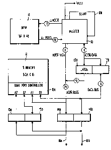
A system employing the present embodiment is shown
30 in FIG. 1, which includes processor 10, which may be a master
processor, in wh;ch case an identical slave procesqor lOa is
also connected to the address and data buses. The slave
processor lOa is used to detect ailures in either the master
10 or slave lOa or in their interconnectlng wiring. Processor
3S 10 receives machine ox "$" instructions and data from S-memory
12 and employs the machine language operators to form an
address to micro memory 11 from which it receives micro ins-
. . .
~a~
7 --
tructions, as will be more fully described below. Processor
10 addresses the main memory array by a 24 bit address bus
which includes an 8 bit high address and a 16 bit low address,
the bus including latch 13a. Data is received and transmitted
by way of a 16 bit data bus via bufers 13b. Buffers 14a and
14b provide for access by processor 10 to interprocessor
address and data buses 16a and 16b respectively. Buffers
L5a and 15b provide for access to S-Memory 12 from other
processors via buses 16a and 16b respectively. Dual port
controller 12a pro~ides arbitration between requests for
- access to S-Memory 12 from processor 10 and any other
processor via ~uses 16a and 16b.
The processor of the present embodiment is illus-
trated in FIG. 2 and includes-external bus interface 20 which
can address main memory 12 of FIG. 1 by way of the high
address bus and the address/data bus, the latter of which
is a bidirectional bus. The processor receives data and
machine instructions from main memory. The external bus
interface, which will be described later in more detail,
- sends portions of machine instruction operators to sequèncer
21b. Sequencer 21b uses that operator to address micro
memory 11 of FIG. 1. In response thereto, micro instructions
are received which are returned to control unit 21a, and
other units, with a portion thereof being used as an address
to nano ~ -~ /
: ~ ~ 2 ~
memory 22, as will be more ~ully described :b~iow. As
indicated in FIG. 2, and as des~ri.bed above, one t~pe of
such micro instruc~ion might be a nano instruction which
is supplied directly to control register 23. Whether the
nano ins~ruction comes from nano memory 21 or from micro
memo~y 11 of ~IG. l, it~ ~arious fields as they reside in
co~rol register 23 are.~hen s~nt ~o arithme~ic logic unit
24 and ~h~ Qther ~unctional units o~ the processor ~o e~ect:
a par~icular operation.
Decoder 23A detects whether the incomlng micro
ins~ruction is a type ~ or a type III micro instructlon~
If it i~ the former, its nano memory address is sent to
nano memQry 22. If the micro instruction is type III, it
is sent direc~ly to control register 23. Decoder 23A
detects ~he type and signals mul~iplexor 25 whether ~o
rec~ive the output o~ nano memory 22 or the inpu~ from
- the micro memory for ~ranser to control register 23.
The various types of micro ins~ructions are
illustrated in ~IGS. 3A-D. The first 4 bits, starting from
20 the left, are employed to indicate the micro instruction
type. In a type I micro instruction o ~IG. 3A, the
next 39 bits corltain se~uence in~ormation, a nano address,
exte~nal operatioIl in~o~:mation and a literal value. Bits
43 ~ough 47 of all types of micro instructions are used to
2S address the B-register file o~ the arithmetic logic unit
that will be more fully described below and bit 48 is a
parity bito
FIG. 3B illus~rates a type II micro instruction
which is employed primarily to supply literal values and
shi~t amount register values to the arithmetic logic unit.
Again, the first four bits indicate the ~ype o micro
instruc:~ion, the r~ex~ ~ix bits are load control informa~ion,
the next 32 bits are either the literal or shi~t amount
;J9~
_ 9 _
value and again bits 43 through 47 are a B-registe$ file
address and bit 48 is a parity bit. .
The type III micro instruction contains as part
of its contents a nano i~struG~ion as was described ab~ve.
I~ thi~ case, the ~irs~ three bits speci~y the ins~ruction
: .type and the nex~ 39 bit~ are the nano instructions. ~gai~,
bits:4~ through 47 are a B~register file addre~s and bit 48
is a pa~ity bit.
A type I micro instruction is illustrated in more
detail in FIG. 3D. A~ was indicated above all m1cro
in~tructions are ~8 bits in width. In FIG. 3D, the firs~
fo.ur bits indicate the micro type. Bits ~ through lS are
co~dition bits with bits S through 8 indicating the condition
that is to be tes~ed, such as adder overflow, and so ~orth.
Bit 9-indicates whether that condition is to be tested to be
true or ~alse. Bit 10 indicates whether an ari~hmetic logic
unit opaxation is conditional or unconditionaL and bits 11
and 12 th~ough lS indicate whether there is to be a
- condition ad~ustment and if the operation is to be conditional.
These condition bits are ~ent dynamlcally to control unit
21a of FIG. 2~
Continuing on with ~he type I format ~ FIG. 3D,
bits 16-18 and 19-21 are sent to se~uencer 21b of ~IG. 2
and indicate the source of the successor micro instruc~ion
address depending upon whether the selected condition tested
is true or false.
3its 22-29 are an 8 bi~ nano address which is
supplied ~y the t~pe I micro instruction to nan~ memory 22
of l~IG. 2 and can selec~ any one of 256 nan~ instructions.
Bits. 30-34 are sent dynamically to external bus interface
20 and control unit 21a of FIG. 2 and speci~y either
an external operation ~r a value to be loaded into the
shift amount ~egister. gits 35 through 42 represent a literal
~2~S 5)~
- 10 -
value and are ei~her s~nt to the li~eral register to be
discussed in relation to control unit ~la or as a br~nch
ad~ress to be sent to sequencer 21b of FIG. 2. As indicated
above, bits 43-47 represent a B-regis~er fiLe address in
the a~i~hmetic logic unit and bit 4~ is a parity bito
FIG. 4 illus~rates he format of ~ nano
i~struction which is received by controL register 23
e~ther ~rom nano memory 2.~ of FIG; 2 or ~rom micro memo~y
11 of FIG~ 1 when a type III micro ins~ruction i5 employed.
~s was indicated above, this nano ins~ruc~ion is made up
o~ gr~ups o~ e~coded control signals which are subsequently
decoded to produce the actual contxol signals. They are
encoded to reduce the size of the nano memory. Since
thes~ various fields co~troL different operations in the
arithmetic logic uni~, which will be more thoroughly discussed
below, ~his discu3sion will cross referenc~ the various
fields o~ nano in~truction a~d the units they opera~ in
t~ arithmetic Logic unitO ~owever, the format of ~he nan~
ins~ruction is being described now to provide a better
understanding of the relationship between a nano instruction
and ~he various u~its o~ the process~r o FIG. 2.
The first our bits o f the nano instruction o~
- FIG. 4 i~dicate the sou~ce for the x input ~o
logic u~i~ 4 0 o ~ FIG . 6 . Bit S through 7 indicate the
source to the y input to l~qic unit 40. Bits 8 through
13 indicate the type of operation to be p~o~ided
by the masker unit 45 o f FIG. 6 b~tween the y i~put and
the logic unit 40. Bits 14 through 18 speci~y the
operation to be perfo~med by the logic uni~. Bits 1~
through 21 indic~te the operation to be performed by the
barrel shifter 46 o F~G. 6 which can shift the output of
logic unit 40 right, le~t, end ~round, and so for~h,
or 3imp1y pa~3 tha~ data on throuqh. Bits 22 through 24
:J~Z~i o(~
- 11
: indicate which one of the A registers 43 o~ FIG. 6 is
to receive data. Bi~s 25 through 27 indicate the source
of the input to ~-regis~er ile 44, FIG. 6. Bits 28
through 30 indicate which memory address registers
32 o~ FIG. S are to receive data. Bits 31 through 34
axe used to ~pecify oth~r d~stinakions as may be required
and bits 35 thxough 39 are mlscellaneous control signals
that wil~ be furt~er desc~ibed below i~ regard to the
oth~r units of ~he processor.
~3'~
.
Exte~nal bus interface 20 of FIG. 2 is shown in
mcre de~ail in FIG. 5. Data is received from the
address/data bus by external register 31 for ~ransmission
. to ALU 24 of FIG. 2, and ~LU reslllts are transmitted to the
address/data bus ~rom the memQ~y information regist~r bus
~I~(L).
In~tr~ction~ are received from the address/data
bus by instruction queue. 30 whic~ can hold up to four 16
bi~ instructions. As will fIrther be discussed in regard
to control u~it 21a o PIG. 2, each 16 bit instruction is
di~ided into four 4 bit field.s IQDA, IQDC, IQDB, and IQDD.
These respective fields are sent to control unit ~la to
fonm B registe~ ~ile addresses o~ mlcro addresses as will
be more thoxoughly described below. In additIon, IQDA and
IQDB can b~ employed to form an 8 bit field which is also
sent to control uni~ 21a to ~orm a mlcro address and the
. entire 16 bit lnst~uc~ion IQ c~n be sent to the ALU.
- S memo~y addresses are received from the
barrel shifter or barrel switch ou~put bus BSW 49 by
30 memory address regist~rs 32 which include three registers
MA* 1 and MAR 2 as well as instruction pointe~ IP, each
of which can be indi~idually selected to transmlt its
content~ to S memory 12 o~ F~G. L by way o an 8 bit
~2~
12 -
address high bus and a 16 bit address bus as was described
above in regard to both FIGI i and FI~. 2. The outpu~
of these registers can also be selected for transfer back
to the ~ and Y adder inputs of ALU 24 o~ PIG. 2, and each
S register caA be independently i~cremented by 1 or by 2.
B~fore describlng the details of con~rol unit
21a and sequencer 21b o~ ~IG. 2, it mlght provide a bet~er
understanding to first describe the functional units o
ALU 24 o~ FIG. 2 which are con~rolled by nanoinstructions
10 of: c~n~rol register 23 of FIG. 2 with the sequence o~
such nanoins~ructions being de~ermined by ~he se~uence.r
21b and con~rol unit 21a. ALU 24 of FIG. 2 is shown in
more de tail iD. FIG. 6 0
In ~IG. 6, logic u~it 40 can receive data inputs
15 fro~ a ~ra iety oi~ sources, designated as bus 48 or the A
regis~er file 43 an~ the B r~gister file 44 by way of X
multiplexor 41 and Y multiplexor 42 respectiv~ly. The
output of ~ multiplexor 42 is supplied to logic unit 40
by way of masker unit 45 ~or reasons that are more thoroughly
described below. The output of logic unit 40 as well as the
: output of X multiplexor 41 are supplied to barrel shifter
46. As was explained above, barrel shi~ter 46 can shift
left or right and end around any number o~ hits ~ositions
as determ~ned by ~he shift aunt amount ~alue s~ecified by
25 the shift amoullt register as was descxibed in relation to
FIG. 3D. The output of ba~rel shifter 46 is supplied to
- memory informa~ion register 47 and also to bar~el shifter
output bus (3SW) 49 ~or ~ansmission either to external bus
interace 20 of FIG. 2 and also contxol unit 21a and sequencer
3 21b o ~ FIG . 2 .
'rhe respective B register to be used is determined
by the B file addres~ of the p~e~ious m1croinstruction and
the other u nits are under the control o f control fields
of a nanoinstruction as described in relation to.FIG. 4.
i '
3~ Z ~ ` r t ~
- 13 -
Thus, the X-Select, ~-Select, masker op~rations, ALU
operations and barre~ switch opera~ions are determined by
control fields that were deseribed in relation to FIG. 4.
All data path widths in FIG. 6 are 32 bits wide
although units o~ FIG~ 6 can be used for a 16 bit wide
data pa~h width under microinstruction control.
. Sequencer 21b o~ F~G. ~ will now be described in
rela~ion to FIG.. 7. Thi3 seq~encer iterates the
mlcroaddresses which address micromemory ll of FIG. 1 to
retrie~e ei~her nanoinstructions or, when requlred,
~icroins~ructions.which, among other thing~, address
nanomemory 22 of FIG. 2 as was described above. Initially,
the sequencing action s~arts by microprogra~ coun~ register
50 (MPCR) being set to zero and upon initiation of an execute
signal, its ~u~pu~ are incremented by 1 by incrementPr 51
and 3e~t to the mic~omemory by way of next address
multiplexor 56 and address la~ch 58. As S ins~ructions
are load~d i~o ~he instruction queue 30 of FIG. 4,
the respective fields o~ thos6! instructions are employed
by control unit 21a o~ FIG. 2 to generate branch
addresses which can either be supplied directly to next
address multiplexor 56 or can be stored in alternate
mic oprog~am count registe~ stac~ 54 by way ~ multiplexor
53. Alternate microinstru~tion addresses can also be
25 entered i~to ~tack 54 ~rom barrel switch autput 49 (~SW)
o~ ~IG. 6. Stac~ 54 is a pushdown stack wherein the last
addre ~ to be entered is the first address to be read out.
Varlous i~puts to next address multiplexor 56
can ei~her come ~rom ~PCR 50, that address incremented by
one by incrementer 51 or incremented by 2 by incrementer
52, the output of A~PC~ stac~ 54 either by way o~ incremeter
5S o~ dir~ctly, or ~xom the branch address genexator o~
~z~
14
con~rol unit 21~ of FIG. 2. Which of these inpu~s is
selec:ted for transm~ssion to address latch 58 is
d~term~ned by successor logic 57 which is activated by a
condition ~ig~al :Erom the current micro~nstruction and
5 one of two 3 bit signals indica~i~g whether a ~rue successor
or ~als2 sUcc~ssor i5 cal~ed ~or, which ~ignals also come
~rom the curren~ ~ype I microins~ructioA. Execution of
microins1:ruction types o~her than type I causes an implicit
selection of ~PCR~l as the nex~ m~croins~ruction address.
Control uni~ 21a o~ ~IG. 2 is shown in detail
i~ FIGS. 8A-D. FigO 8 mereLy illustrates the four sec~ions
of: the co~trol unit whic:h ~nclude the literal register,
t:he condition test and adjust, m~scellaneous control
registers and address modifiers.
FIG.. 8~ is a ~loc}c diagram of the logi.c which
gen~rates bcth the B ~ile add.ress for B register file 44 of
~IG. 5 and also the b:ra~ch add~ess for seque~ce~ ~lb o~
FI~. 2 and FIG. 7. TherQ are ~o inpu~s from the cll rent type
I m~Lcroinstruction to this logic. One is the B file address
~0 which is 5 bits and also a 16 bit b~anch address, both o
which come from the type I microinstruction of FIG. 3D. The
B ~ile address bit~ in that microinstruc~ion are bits 4~-47
and the 16 bit branch address is obtained from bits 30-42
and also 13, 14 and 15 when those fields are used to supply a
branch address~ Modifications to these lnputs come from
external bus interface 20 of FIG. 2 which is shown ~n detail
in ~IG. 5, or from the least significant 16 bits of barxel
switch output bus 49 o~ FIG~ our bit fields IQDAt~IQDB,
IQDC and IQDD and BSW outpu~ 49 are used to dify B register
~ile addresses and~or mlcroinstruction branch addresses
supplied by the current type I microinstructio~`. The
concatenation o~ IQDA and IQDB is used to modify
micro m~truction branch addr~sses supplied by the current
t~pe I microlnstruction.
~2~
- 15 -
FIG. 8B illus~rates the miscellaneous control
registers, all of which can be loaded from barrel shift
ou~put 49 of FIG. 6 with values generated by logic unit
40. S~me of these regis~ers can be loaded from other
sources, and perform speci~ic functions, as will now be
dascxib~d.
IQ sta~us register 61 r~ceives a 3 bit IQ sta~us
sign21 which indicates the n ~ er o~ bytes in the
i~truc~ion ~ueue o external bus interface of FIG. 5.
~5 indicated above, it aLs~ receives values generated by
the logic unit 56 of FIG. 6 and its output goes both .to
the X adder input and to the IQ con~rols.
S s~atu~ register 62 receives an enable S status
signal from ~he miscellaneous field of the nanoinstruction
format of ~IG. 4 a~d also receives 4 bits represen~ing
ALU conditio~ which re~ult ~rom an ALU operation.
~ as~ ~agi~te~ 63 e~ables cer~ain status conditions
to become an iAterrupt re~uest signal.
optio~s register 64 receives among other
thi~gs literal values from either a type I or type~II
microinstruction which literal values come from the
iiteraL ~egister to be describe~d below and are supplied
to options regi~ter 64 by way o~ the ALU and barrel
switch output bu~ 49. Its outp~t gs~es to the X adder input
25 and to cer~ain control logic elements to enable specific
operating modes.
Shi~t amount register 65 receives a shift
amount value from ~che iogic unit by way o f barrel
switch outpu~ 49 but also can receive shi~t ~moun~
values from the shif~ amount field of a type I or ~ype II .
microinstruc~ion o ~IGS. 3D and ~B and counter 6~ can receive
values- ~rom b~rrel switch output 49 and also from the
literal regis~er to be discussed below in rega~d to FIG. 8D~
r~~ t~ ,~
- 16 -
FIG. 8C shows the condition selec~ ~ogic 69
and flag register 700 Condition ~lect logic 69 receives
input from coun~er overflow outpu~ o counter 66 o~ F~G. 8B
as well as various exter~al conditions, ALU conditions and
S cer~ain bits of tha flags register 70. Combinations o~
th~se signa~s are selected by the condition selec~ field,
bit~ 5-11, of a type I microinstruction and out~u~s the
selected conditions to seque~cer 21b o FIG. 2, ALU 24
o~ FIG. ~ a~d to the flag register 70 ~o modify the value
~ cextaln bi~s of the flags register in accordance with
th~ condition adju~ command from a.type I microinstruction,
bits 12-15, of FIG. 3~.
Flags register 70 receives as its Lnput signals
- generated by logic unit 40 of FIG. 6. The value of ~he bits
of the flags regi~ter is adjus~ed according to the condition
adjust command described above.
FIG. 8D illus~rat~s the literal register in con~rol
unit 21a a~.FIG. 2 which can receive 8 and 16 bit literal values
from a type I microinstructio~ of FIG. 3D as well as a 32 bit
literaL ~alue from a t~pe II ~icroinstruction as illustrated in
FIG. 3B. ~o this end, register 67a and re~ister 67b are each
a bit registers while register 67c is a 16 bit regis~er.
In addition to the ~unctions and various operations
that have been described ab~e, the present embodlment features
two ope~ation tha~ are particula~ly useful in pro~idinq
t~e flexibility of the processor of the present embodiment.
As~was indicated above, one o~ theqe featur~s is the
ahility of th~ arithmetic logic unit of FIG. 6 to ~mploy
either a 32 bit or 16 bit data path width under program
control. The manner in which this is done is ~hat the
programmer loads literal register af FIG~ 8D with the
appropriate value to indicate whether a 16 bit bus or
32 bit bus is to be employed. ~his is done ~ith a type I
mic~oi~s~ruc~1on which is followed by a type III .
~ 17 -
microinstruGtion or nanoinstruction which transfers thevalue of ~hat literal register by way of the logic unit and
the barrel switch output bus ~o options register 64 o~
~IG. 8B. Thi~ a~ects ~he logic unit's most significant
bit condition and carry ou~ and the all-zeroes and all-ones
de~ection logic. The barrel swi~ch operation is also a~fected,
sincs end around shif~ing is different Ln 16 bi~ and 32-bit
modes~ Another feature of the present emxxhmEnt is the
ability ~f the arithm~tic logic unit to isolate di~ferent
~ields Ln one clock time. This is achieved by supplying the
data word empLoying field to be isolated to the Y multiplexor
42 o~ ~IG. 6 and to masker unit 45 which, under control of
the current nanoinstruction, mas~s out that portion of the
da~a word to the left o~ the ield to be isolated. The
remaining portio~ of the data word is upplied to the barrel
shifter 46 by way o~ logic unit 40 where it is shif~ed to the
right end off to remn~e that portion of the da~a w~rd to the
right of the desired ield to be isolated~
:EPI~OGUE
~ micropr~grammed processing system has been
described which employs ~wo le~els of sub-instruction
sets, namely m~cro~ns~ructions which are used either
to address a nanoinstruction ~/mory or con~rol store
of the processor or to supply such a nanoins ' ~uction directly
to the conttol register of the procQssor. In this manner,
only a limlted ~mber o~ nanoins~ruc~ions need be stored
~ a read o~ly memory within the procass~r that is placed
on arl integrated circu~t chip. This allows for further
utilizatiol~ o~ t~e chip to include a 32 bit data bus
30 processor and achieve other ~unctions. Under mic~oprogram
control, the processor can be placed in either a 32 bit
- 18 - .
data bus or 16 bit data bus mode and the processor is also
provided with a masker unit and barrel shifter unit that
can isolate a field in a data word in one clock time.
It will be seen that there is described an improved
processor that can employ a fully expanded set of nano in-
structions. The processor has a fully expanded nano instruc-
tion set so as to provide greater flexibility and utilize
: all the capabilities of the processor's functional units.
The described processor is implemented in an in-
tegrated circuit chip which processor is driven by two levelsof subinstructions, namely micro instructions and nano ins-
truc~ions, the latter of which are -
encoded groups of control signals (although they need
be encoded) that actually drive the various functionaL
L5 units of the. processor~ A select group of such nano instruc-
tions are.stored on the integrated circuit chip in a nano
memory, which is addressed by respective micro instructions
from a random access micro instruction memory. In the
described embodiment, the micro memo~y is on a separate
integrated circuit chip. In order to limit the size of
the nano memory, only a sele.cted group of nano instr~ctions
are stored therein with the normal routine nano instructions
being supplied as part of the micro instruction code stream.
With this reduced nano memory, it is possible to use a data
bus in the processor of 32 bits; however, for certain appli-
cations, only 16 of these bits may be used, thereby short-
ening the data path width of the processor. This selection
be~ween the 16 bit and the 32 bit data path is under the
control of a micro level instruc~ion source so as to be pro-
gr~¢mable. Furthermore, the processor can isolate a selectedfield in a data word during one clocktime under microprogram
controlO
A eature then of the embodiment is a processor
having two levels o subinstructions, with the processor
data bus being selectable as either a 16 bit or 32 bit wide
bus under nanoprogram control.
Although one embodiment o~ the present invention
has been described, it will be apparent to those skilled in
the art that variations and modifications may be made there~
in without departing from the spirit and the scope of the
invention as claimed.
.
30 .
, ' ,