Note: Descriptions are shown in the official language in which they were submitted.
~L~67t91~5
A DEVI OE FOR DETECTING AND LOCALIZING NEUTRAL PARTICLES, AND
APPLICATION THEREOF
Tha present invention relates to a device Eor detecting
and localizing neutral particles such as X photon~, gamma
photons, or neutrons, the device comprising a~ least one sensor
in the form of a gas-filled enclosure which is permeable to
said neutral particles and which contains at least one
converter capable of emitting ionizing particles under the
impact of said neutral particles in order to give rise to
charged particles by ionizing the gas, together with a detector
member which is electrically polarized relative to said
converter in such a ma.nner as to attract said charged particles
with sufficient force to give rise to an avalanche phanomenon.
BACKGROUND OF THE INVENTION
A prior art device of this type is descrlbed in British
published patent application No. GB 2 000 632.
The simplest embodiments of devices for detecting neutral
particles comprise an anode wire and a cathode which acts as a
converter, wlth the anode wire and the cathode being disposed
in tha vicinity of each other, and wlth the assembly being
~ contained in a gas-filled enclosure.
: An example of a de.t~¢tor having thi3 structure i
describad in the article at page 577 of "Review o Scientific
: Instruments", ~ol. 50, No. 5 (197g).
Regardles~ of the way in whic~ such detector~ operate, tha
function of the c~nverter includecl thereln is to ~mit ionizing
particles under the impact of neutral particles, and more
specifically to emlt fast or "primaryN electrons. The k~netic
energy of such fast electrons is cJreater than the ionlzation
enerc3y of the atoms or molecules of the gas and i8 ~ometimes so
high that these electrons cannot be eff0ctlvely guided bowards
the anode by the electric fleld establishsd insid~ ~he
enclosura.
In contrast, by ionizing tha gas these primary eleat~ons
create electron/positive ion pairs, and the electron~ created
in this way are referr0d to aQ "secondary electnons". The
secondary electrons migrate towards the anode while the
positive ion5 migrate towards the cathode.
- $~
~L2679~5
An electric charge whose ma~nitude depen~s on the number
of sacondary electrons is thus collected a-t -the anode. An
appropriate circuit ~or "channel") connected to the anode
delivers a measurement signal proportional to the electric
char~e collected by the anode, and consequently representative
of the energy or the intensity of the observed phenomenon.
In conventional m~nner, the collected charge may be
detected ~ither directly or indirectly. When det~cted
indirectly, th~ electric charge is allowed to flow along a
conductor and detection consists in detecting the resulting
electric current.
Apart from these common characteristics, neutral particle
dstectors are very diverse, and are generally classified into
two main types, depending on whether or not they make use of
the "Townsend avalanche" phenomenon.
This phenomenon, which is well known to the person skilled
in the art, appears when the electric field in the vicinlty o
the anode is sufficiently intense to accelerate the secondary
electrons so that the kinetic energy which they acquire ~atween
tw~ collisions becomes greater than the ionization energy of
the atoms or the molecule~ of the gas.
Under these condit$ons, the secondary electrons ma~ in
turn craate further secondary electrons which themselves
participate in an avalanche phenomenon as the~ mova towards the
anode, with the avalanche ceasing only when all of the free
electrons have been collected by the anode.
This multiplicative effect on the det~cted electrons gives
rise to significant ampliication of the measurement signal,
e.~. by aq much as 107, thereby very substantially improving
the signal/noise ratio.
Undsr good conditi~ns~ th~ number of secondary electrons
can be maintained at a/determined ratio to the number of
primary electrons. Detectors oparating under such condition
are called "proportional counters".
~owever, ths multiplication actor of tha avalanche
phenomenon can only be controlled to a limited degree of
accuracy, and in some applicat~ons it is preerable to provide
s
detactors which do not make use of the avalanche phenomenon.
This is true, in particular, of "ionization chamber" detectors
and examples thereof are giv~n in the above-mentioned article
in "Review of Scientific Instruments", in British patent No. GB
1 578 325, and in French patent No. FR 2 503 381. These
instruments generally detect radiation under metrological
conditions so long as the charge accumulated on the anode is
measurable, which requires the neutral particle radiation to be
intense or the duration of measurement to be long.
That is why ionization chambers cannot be usod in imaging,
or in localizing particles, except under very s~ecital radiation
conditions. In particular, they cannot be used/if the energy
of the radiation to be detected is about 80 keV or rather less
than said value. Further, the application of ionization
chambers to imaging gives rise to complex devices, since each
chamber provides only one point (or "pixel") of the image, as
shown in French patent FR 2 503 381.
Avalanche detectors which are substantially better adapted
than ionization chambers to such applications are well ~nown to
the person skilled in the art of imaging or in the art of
localizing particles.
An example of a p~oportional counter applied to two-
dimensional image acquisition is given in the artlcle on page
157 of "IEEE ~ransactions on Nuclaar Science", vol. 27, No. 1
(February 1980).
mis detector comprises a twe-dimensional n~t~ork of anode
wires associated with bundles of lead oxide crystal tubes
acting as converter~ and disposed perpendicularly to the plane
- of the anode network. The angle of incidence of the neutral
particlo radiation on the det~ctor i~ close to 90 and the
conversion efficiency o~ the detec~or is fairly independent o~
the angle of incidence and remains les~ than 8~.
Another proportional counter for direct acquisiticn of
tw~-dimensional images is de9cribad in British patent number
2 000 632. mis device, like the above de~ice, belongs to the
class o~ apparatuses known as multi-wire proportional chambars
and is in*ended for detecting radiation impingeing thereon at
~6~4~
72989-1
an incidence perpendicular to its plane. It comprlses two
cathodes .tn the form of s~rips and constitutiny solld converkers
together with an anode constituted by a plane o~ wires which are
electrically interconnected.
The strips of cathodes are associated with delay lines
which are in turn connected to a time analysis circuit.
Other than the fact that this detector requires a
complex analysis circuit, and the fact that its conversion
efficiency cannot be very high, it necessarily leads to rather
long image acquisition ~imes, thexeby limiting its application to
the formation of quasi-static images, for example to scintigraphy.
In this context, the essential aim of the invention is
to provide a device for detecting and localizing neutral
particles, said device being substantially more efflcient than
prior multi-wire proportional chambers, ln particular when the
; energy of the neutral particles is substantially greater than 50
keV.
SU~ARY OF TH13 I~VE~TION
According to a broad aspect of the lnvention there is
provided a device for de~ecting and localizlng neutral particles
comprising,
at least one sensor in the form of a gas-filled enclosure
which ls permeable to said neutral particles and which contalns at
least one converter capable of emitting ionizing particles under
the impact of said neutral particles in order to give rise to
charged particles by lonlz1ng the gas, together with detecting
means comprislng charge multiplication means wh1ch are
;7~
72989-1
electrically polarized relative to sald converter in such a manner
as to attract said charged particles wlth suffici~nt ~orce to yive
rise to an avalanche phenomenon, the device including the
improvement wherein the particles propagating relative to said
sensor following a prede~ermined average direction and the
converter comprises a plate of solid material at an angle of less
than 10 to said average direction and wherein sald detecting
means comprise a network of electrically conductive elongate
charge collecting means which are substantially parallel to one
another and to the plate of the converter, and which are connected
to circuits for formlng a one-dimensional image corresponding to
the distribution o neutral particle intensity along a direction
perpendicular to the projection on the plane of the converter
plate of said average direction of particle propagation.
According to another ~road aspect of the invention there
is provided a method of detecting and localizing neutral
particles, comprising the steps of:
; propagating a flow of said neutral particles from a source thereof along a predetermined average direction;
receiving a portion of said flow of neutral particles at a
gas-filled sensor containing a converter plate inclined at less
~han 10 to said average direction and emitting from said
converter a corresponding flow of ionizing particles to generate
charged particles of ionized gas;
amplifying said flow of charged particles by charge
multiplication means which are electrically polarized relative to
said converter plate to attract said charged particles with
.,
~6,J ~I~S
7~89-1
sufficient force to give rlse to an avalanche phenomenon; and
detecting a distribution of charged particles along a
direction perpendicular to a pro~ection on a plane of said
converter plate o~ an average direction of propagation of said
neutral particles and generating a corresponding signal
representative of a distribution of neutral particle intensity
along said perpendicular direction.
Although, a priori the plate constituting the converter
may be plane, warped, dished or corrugated in shape, a plane shape
is genqrally most suitable.
One of the essential novel features of the invention
lies in the fact that it provides a sensor which, while being
simple in structure and suitable for industrial manufacture~
never-the-less combines the quallties of proportional chambers and
the advantages of a solid converter for application to localizing
particles. The advantages of a solid converter include those
known prior to the invention and those shown up by the
invention,and they are related to the use of a glancing incidence.
In the past, ~he person skilled in the arts of imagin~
and o~ localizing particles has been in the habit either of
associating each pixel of an image with a specific detector of the
ionization chamber type, as shown by French patent number FR 2 503
381 and British patent No. GB 1 578 325, or else of forming an
image in a plane substantially perpendicular to the direction of
propagation o~ particles to be localized by associating each anode
wire or strip to an entire row (line or column) of image pixels,
as shown ln British patent number GB 2 000 632 and the above-
5a
B
72989~1specifled article ln the journal "I~EE Transactions on Nuclear
Science". In contrast, the present :Lnvention propo~es using an
avalanche detector to form an imaye in a plane at a glanciny
incidence relative to the directlon of particle propagation, and
associating a row of pixels with an entire set of elongate
detector elements (wires or strips).
The resolution of the detector in accordance with khe
invention is optimal if the elongate detector elements are wires
which are electrically insulated from one another and extend taut
parallel to the projection on the plane of the converter of the
average direction of particle propagation.
5b
7~S
Each wire is then connected to a separate electronic
charge detection circuit (or channal) with the one-dimensional
image being formed by ~he set of output signals fran said
circuits.
These electronic circuits (or channels) are known E~ se
and may, for example, be of the type used with multi-wire
proportional chambers.
Good results may be obtained in the detection of X photons
or gamma photons when tha converter contains a material whose
13 atomic number is not less than 25.
It is also advantageous, in p OEticular for detecting
neutrons, for the converter to contain a material having an
effective interaction section with neutral particles o~ not
less than one millibarn, where a barn is e~ual to 10~24cm2.
Of the materials that may be used, the conYerter
preferably contains a material selected from the group
constituted by: tungsten, tantalum, laad, cadmium, gadolinium,
boron, samarium, europium, lithium, dysprosium, rhodium,
berylliwn, carbon, goldt silver, lanthanum, depleted uranium,
.20 platinum, thalium, niobium, molybdenum, nickel, copper, cobalt,
iron, i~idi~m, mercury, indium, man~anese, hydr~gen, deuterium,
nitrogen, oxygen, and chlorine.
~ y way of more precise example, the convertar may be not
more than 2 mlllimeters thick and may ha~e at least soma points
on one of its faces making an angle of nDt more than 5 with
the average direction o~ propagatlon of the neutral particles.
For photons having an enargy of 400 ksV for example, the
converter may be a plate of tantalum havlng a thickness o~ not
more than 200 micron~ and having at least some points on one of
its faces making an angle of not more than 2 with the averaye
direction of neutral partlcle propagation.
The detector member may be constituted by single strlps of
appr~priate width i~ the device is used in low count rate
applicatio~s and is used in PPAC (parallel plate avalanche
counter) mode or in pseudo-PPAC mcde, i.e. if it is not used in
proportlonal mode.
:a26~
When maximum image definitiorl is not required, the
elongate detector elements ma~ be cons-tituted by an
electrically conductive material of fairly high resistance, in
which case these elements are stretched parallel to the plane
of the converter pla-te and are disposed perpendicularly to the
projection on the plane of said plate of the average
propagation direction of the neutral particles. In this case
the elements are electrically connected to each other at each
end and the ends are themselves connected to an electronic
channel for detecting charge. With such an assembly, neutral
particles are localized along the datector elements by virtue
of the way the current produced by the collected charges is
distributed between the two electron ic channels.
For e~ample, ths distance between pairs of adJacent wires
and the distance betwe~n each wire and the converter may be
less than 15 mlllimeters.
I'he efficiency of the device ls further improved if it is
provided with an additional plane el~ctrode rais~d to
substantially the same electrical potential as the converter
and disposed p~rallel thereto but on the other side of the
network of wires, and if the detector member include~ a net~rk
of wires and an additional olectrode on each sida o the
convarter.
Thi.~ arrangement axtract~ even greater adv2ntage from the
glancin~ incidence disposition of the converter relative to the
direction of particle propagation. Thls arrangemant make~ it
possible to use a very thln oonverter thereby makin~ it highly
probable that primary electrons will also be emitted from the
surface of the converter which ls not directly sub~ect8d to
neutral partlcle radiation. The additional secondary electrons
created by such primary alectrons are also collected.
In order to contn~l the operating par~meters of the device
(which parameters are greatly influenced b~ the naturc of the
medium separat~ng the converter from tha detector member), tha
enclosure enclosing the convertsr and the detector m~mber is at
least partially filled with an inert gas.
~Z67~5
The pressure of the gas in this enclosure ls preferably
less than lO6 p~scals, and the electrical potential difference
between the detector member and the converter is preferably
less than 30 kV.
Advantageously, the device includes a bracket holding the
converter and the detector member at an angle to a reference
axis related to the external shape of the enclosure, with said
angle being suitable for obtaining the desired orientation of
the converter relative to the average direction of neutral
particle propagation when said reference axis i5 itself
directly pointed in said dirsction.
The advantages of a device in accordance with the
invention for detecting and localizing neutral particles ara
particularly apparent when the device is applied to imaging,
i.e. when it is used for obtaining an image or at least a
partial image of a body.
When a body is irradiated by a source of nsutral
particles, the radiation passing through the body is attenuated
as a function of the nature of the material through which the
radiation passes and of the mass of ~aid material, thereby
giving rise to a corrosponding spatial intensity distribution
which can be revealed by a sensor of 1:he kind described above.
In such applications, a device ln accordance wi$h the
1nvention thus generally comprises at least one source of
2~ neutral particles which is located at a distance ~rom th2
sen~or(s), with the sensor(s) belng orient~d to take tha
directlon of the axis between the sensor(s) and the ~ource as
the average direction of neutral particle propagation~
The device then preferably includes at least one neutral
particle collimator associated with a correspondlng sensor,
said collimator having a slot for restricting the beam of
particles recelved from the source to a flat beam centered on
the average dir~ction of propagation and intersecting the plane
of the sansor converter in a direction substantially
perpendicular to said average dlrection of propagation.
The device may include a frame on which a plurality of
sensors are mounted.
~Z6~
g
In this case, the sensors axa advantageously disposed ln a
staggered arrangement on the fr~n~ so that their respective
converters, when considered as a whole, overlap sufficiently to
interc~pt the entire flat beam of neutral particles coming from
the source.
Also, the frame is preferably enveloping in shape, for
example L-shaped, U-shaped, or arcuate, with the source being
disposed at a distance from the frame but within its enveloping
shape.
~he device may lnclude a plurality of sources of neutral
particles or a source capable of being placed in a plurality of
different positions. In this case, the sensors may ba
rotatably mounted on the frame so as to be pointable to one or
other of the sources of neutral particles or to ona or other of
the possible positions for a single source.
The sansor may be provided with a converter having an area
of substantially more than S00 cm2 associated with two networks
of wires extending along two orthc~onal directions, so as to be
able to provide a two-dimensional image of an irradiated body
using the above-descrlbed elect~ostatic induction technlque.
Also, the device may comprise a stack of planes
constituted by alternating converters and detector members.
These planes are parallel to one another and are placed as
described above at a slancing incidenc~ relative to the
direction of neutral particle propacJation.
As mentioned above, each detec:tor member may cc~prise a
series of N c~nductive strips (or inclividually-insulated wires)
extending parallel to the pro~ection, on the plane of the
corresponding con~erter of the avera~e propagation direction of
the neutral particles. If the device cc~prises M detector
membars, it i~ suitable for giving a ~wo-dimensional lmage of
an irradiated body corresponding to a matrix of N x M elements.
However, since the geometry of th9 sensor described aboYe
is better adapted to makin~ one-dimensional images, a simpler
solution for obtaining a two-dimensional image of a bo~y of
considerable size and/or volume (e.g. several tens of cubio
meters) consists in forming an lmage of a section o~ the body
~;Z 6741~5
to be examined, in scanning the body to bs examined, i.e.
forming successive images of successive sections, and in
recording the various images obtained over a period of time.
Such a technique is conventional in imaging.
In this case, the body may be moved relative to the sensor
or to the source~ or preferably relative to both the sensor and
the source.
A device in accordance with the invention can be used to
obtain an i~age of a dense object pressnting a thickness of
more than one centimeter of metal to the passage of neutral
particles, and it may bs used with bodies of iron or steel
presentin~ a thickne.ss of up to about 60 centimeters.
The device can thus be used for making images of dense and
bulky ob;ects such as containers.
In this type of application, it is convenient to use X
photons or gamma photons. Their energy is equal to not less
than 50 keV, for example, and preferably lies in the ran~e 250
keV to 2 ~eV, and is typically about 350 keV to 750 keV.
There are numerous advantages to a dsvice in accordance
with the invention.
The sensor efficiency is very high, and is about 30% with
radiation of 400 keV, thereby makir~ it possible to obtain a
hlghly-contrasted image of an examined ob~ect.
Also, by virtue of thls high efficiQncy, lt i~ nDt
necessary to make use of very ener~etlc radiation, even when
forming images of dense and bulky ob~ects as mentioned above.
As a result the precautlons which need to be taken to provide
protection again radiation remain moderate and the sources
th~mselvss, l.e. typically X-ray generator~, remain reasonable
in volume ~nd expense. The angle of emisslon of the X-ray-
~
emitted by these generators remain~ ~airly larye and this makes
lt possible to irradiata a relatlvely bulky ob~ect in a
relatively small space, l.e. in an installation or a building
of relatlvely small s~ze.
BRIEF DESCRIPTION OF THE DRAWINGS
Embodiments of the lnvention, and more particularly
; embod~ments adapted to detecting photons, ara described balow
:~6, ~
11
by way of example with reference to the accompanying drawings,in which:
Figure 1 is a diagrammatic fragmentary section through a
sensor used in a device in accordanc~ with -the invention, with
this view being used to illustrat~ tha principle of sensor
operation;
Figure 2 is a fragmentary exploded view of the sensor;
Figure 3 is a section through an entire sensor;
Figure 4 is a partially-cutaway perspective view of an
industrial imaging installation using a device in accordance
with the invention; and
Figures 5a and 5b show details oP the Figure 4
installation.
MORE DETAILED DESCRIPTION
The invention relates to a device comprising at least one
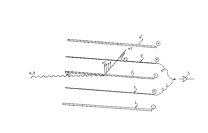
sensor 1 (shown fully in Figure 3) including a converter 2 (see
Figure 1) and a detector mPmber which is itself built up from a
plurality of elements 3, 3', 4, 4', described bel~w.
The sensor is lntended to detect and to localize neutral
particles irradiating it, such as X photons, gamma photons, or
neutrons. The average direction oE propagation of these
particles as symbolized ln F~gure 1 by a wavy line, is assumed
to be substantially fixed relative to the sensor, at least
during detection. The particles are assumed to be propagating
in a shaet parpendlcular to the plane o~ Figure 1 with the
sheet cutting the plane of the fi~re substantially along the
wavy line.
The converter 2 i9 a plate of high atomic number material,
for example tantalum, disposed at a glancing incidence relative
to the direction of propagation of the neutral particles.
Thus, by way of example, the angle alpha betweQn said plate and
said direction may be equal to 1. In Figures 1 and 3 the
converter is assumed to extend in a plane perpendicular to the
plane oP the figures.
For ~xample, the converter may be 30 centimeters long (the
lon~est dimansion visible in Figures 1 and 33, 1~ centimeters
wide (the dimension which is perpendicular or practically
~2674~5
1~
perpendicular to the plane of each of Figures 1 to 3), and 70
microns thick.
Although not essential, it is con~enient to use a
converter which is plane. If the plate constituting the
converter is not sufficiently rigid, it may be glued to a rigid
support but this gives rise to a loss of efficiency of about
20% to about 50%, gi~en that electrons are no longer detected
in one of the two half spaces.
As shown in Figure 1, th~ smaller the angle alpha, the
greater the distance that an incident particle must travel
through the converter for a given thickness of converter.
For an angle alpha of 1 and a converter thickness of 70
microns, this distance is about 4000 microns, i.e. 4 mm.
On either side of the co~verter 2 there is a respectiYa
networ~ of conductive wires 3 and 3', each raised to an
electric potential which ls different from the potential to
which the converter 2 is raised.
For example, the networks of wires 3 and 3' may be at
ground potential while the con~erter is raised to a negative
potential of 2 kV to 3 kV.
The converter responds to the impact of an incident
neutral particle by virtue of the photoelectric effect, or the
~cmpton effect, or by pair creation, to li~erate at least one
high-energy primary electron e~l capable of ionizing the gas and
creating electron/ion pairs. The s~econdary electrons e~2
created ln thls way are attracted, by virtue of tha~r electric
charge, tGward~ one or other of the two netwsr~s of wires 3 and
3', and in turn they create further secondary electrons e~2.
In the terminology applicable to the art, the charged
particles, and in particular the secondary electrons collected
on the anode, are frequently referred to as "charges".
While the angle alpha betwe~n the incident partlcles and
the converter 2 is small, the angle of amission of the elactrons
e~l relatlve to the converter, may be larga, and practically equal
to 90, so that the path which these electr~ns hav~ to ~ollow
inside the converter befors being removed therefrom i~ very
sh~rt relative to the 4 millin~ter~ of virtual thickness which
the converter offers to the inoident radiation.
:
~2~
13
The networks of anode wires 3 and 3' enable the signal to
be amplified by multiplying the charges due to the Townsend
avalanche phenomenon, and they also serve to loealize a charge
received in this way. ~he wires are situated on either side of
the con~erter 2 and extend in planes parallel thereto, i.e. in
respective planes perpendicular to the plane of Figure 1.
The wires in the two networks 3 and 3' are also parallel
to the projection onto the plane of the plate 2 of the average
direction of propagation of the neutral particles. Since this
average direction corresponds in Figure 1 to the direction of
the wavy line, the projection of this direction onto the plate
2 coincides in Figure 1 with the bottom adge of the highly
elongate rectangle representing the right cross-section of said
plate, and the wires of the two networks 3 and 3' extend
p OE allel to said projection.
Al 1 of the wire in the natworks 3 and 3' are raised to
the sams electric potential, however each wire in each network
is electrically insulated from all th9 other wires of the same
ne~work. In contrast, each wire of each network may ~as shown
in Figura 1) be connected to the wire of the other network
which occupies a s ~ netrical position relative to the plane of
the converter in order to constitute a pair of detector wlres
therewith. Each of these pai~ of detector wires in the
networks 3 and 3' i9 connected/a sspaxate electron/detector
channel which is symbolized by an ~nplifier 5. Each channel
amplif1e~ the electric current corresponding to the charges e~
collected on the pair~ of wire~ wlth which it is associated.
Thus, the set of electron~channels deliver a set of electrical
signals representative of an image of the intenslty distribution
of the neutral particles in a direct~o~ perpendicular to the
plane of Figure 1.
These signals are used, as i~ well known to the person
skllled in the art, to provlde a final video image.
The sensor detector member also ~omprises t~o additional
plane electrodes 4 and 4' which are disposed parallel to the
converter 2 and the netwDrks 3 and 3' and on the opposite sldes
of the netwDrks 3 and 3' from the converter. These additional
~2~4~S
14
electrodes ar~ raised to the same potential as the converter,
i.e. in the pr~sent case to a negative potential of 2 kV to 3 kV.
Although not essential, these additional electrodes
provide improved multiplication and improved charge collection,
and they also cancel the electrostatic forces acting on the
anode wires of the networ~s 3 and 3' which could otherwise
curve the wires and thus alter the behavior of the sensor.
Figure 2 gives a better three-dime~sional represantation
of the overall structure of the converter/detector member
lQ assambly~
Figure 2 shows the converter 2 in the middle, and in the
embodiment shown the converter is constituted by a tantalum
plate haYing the dimensions 30 cm x 16 cm x 70 micrometers.
This plate is stretched be~ween two rectangular frames of
stainless steel 6 and 7 each of which 1.5 mm thick.
The frame 7, which is the lower frame in Figure 2, is
missing the edge on the side of the converter which receives
the neutral particle radiation, as symbolized by arrows. mis
edge is replaced by an elongate elQment 7a made of a material
ZO which is more permeable to neutral particles than is steel, for
example it may be made of glass fiber reinforced epoxy resin.
On either sids of assembly 2-6-7-7a constituted by the
converter and its frames, there are tw~ plates 8 and 9 which
support anode wires such as 3a which constitute the networks 3
and 3'. ~or ~he purposes o~ clarifyin3 the drawlng, the
network 3 has not bsen shown ~ n Figure 2.
These plates 8 and 9 aro longer than the frames 6 and 7
and are made of a rigid insulating ~aterial which i-~ permeable
to the neutral particles. Glass $iber reinforc~d epo~y resin
plates of the klnd generally used ~or printed clrcuit cards are
perfsctly suitable.
Each of these plates 8 and 9 is 1.5 mm thick and is
pierced by a corresponding wlndDw 8a or 9a which is smaller in
size than the frame~ 6 and 7.
The anode wlreQ such as 3'a of the nctwork 3' are
stretched over the ~op sur~ace (as sh~wn in FlgNre 2) o~ the
plate 8 above ~he window 8a.
~z~ s
These wires may be made o~ stainles~ steel or gold-plated
tungst~n, for example, and they are about 50 micrometers in
diameter. They are thus stretched parallel to one another with
the distance between pairs of adjacent wires being about 2.5 mm,
for example.
These wires are fixed to the plate 8 by any suitable
means, for example by spot welds 10.
These wires are electricall~ insulated from one another by
virtue of the very high resistivity of the frame 8 and they are
independently connected to separate connection cells in a
connector 11 fi~ed to the end of the plate 8.
The two wires extending along respective edges of the
window 8a are of greater diameter than the other wires, for
example they may be 70 microns in diameter, and they are not
connected to the connector 11. mis feature is not
specifically shcwn in Figure 2 for reasons of clarity, but
serves to pr~vide a uniform electric field for all of the anode
wires actually connected to the connector ll.
The network of wires 3 on the plate 9 ls made in an
entirely similar manner and is disposed symmetrically about the
plane of the converter 2.
In other words, with reference to the disposition in
figure 2, the wires of the network 3 are stretch~d over the
hidden face of the plate 9.
The only difference lies in the connections to the
natworks of wires 3 and 3'.
For example, a~ shown in Figure 2, the plate 9 is shorter
than the plate 8 and wires such a~ 3a, and 3b, of the network 3
are separately connected to the wires 3'a, 3'b of tha network
3' which occupy symmetrical position~ about the plane of the
converter 2 in the vicinity of the point where 8aid wires of
the network 3' are connected to the conn~ctor ll. Thus,
althouyh the connector ll is unted on the plate 8, it also
serves to pro~ide connections to the wires o~ the netwD~k 3
mounted on the plate 9.
The additional plane electrodes 4 and 4' are symmetrically
disposed on either gide of the above-described assembly 2-6-7-
~ o ~
16
8-9 at a distance from the corresponding networks 3 and 3' which
is set to 3 ~m by thickness spacer members l~aS, 12b, 13a, and 13b.
The additional electrodes may be made of stainless steal
plates, -for example and they are also referred to as "cathodes"
because of their negative electrical bias, one of whose
functions is to re~lrn electrons torn from the converter back
towards the anode wires of the networks 3 and 3'.
Above the cathode 4' (as shown in Figurs 2) there is an
insulating plate i4 whose insulating function is mora readily
understood with reference to Figure 3.
Finally, a spacer 15 is disposed between the plates 8 and 9
in order to prevent any relative movement between said plates.
The stack described with reference to figure 2 is
assembled by any suitable means, for example by a NYLON screw
passing through the stacked elQments and clamping them together.
The completed assembly is mounted on a brarket 16 (see
Figure 3) with the plate 14 insulating the cathode from the
bracket in case the bracket is made of metal.
The bracket 16 is fixed by any suitable m~ans, for example
~ bolts 17 to the base 18a of a gas-tight enclos~re 18.
The enclosure 18 is essentially constituted by a rectang-
ular box l~b which is fixed to th9 base 18a by means of suitable
members such as bolts l9a, l9b and nuts 20a, 20b wlth a sealing
gasket 21 ensuring that the anclosure is indeed gas-tight.
The enclosure is made of a material which i8 permeable to
neutral particles and which is mecha~lcally strong, e.g. alumin~m.
In Figure 3, reference 22 deslgnates the longltudinal axis
of symmetry of th~ external rectangular æhape o~ the enclosure 18.
The lines where this a~is passeq through the base 18a and
the facing end of the box 18b are readily detenmined by slmple
length measurements.
In order to orient the converter properly relative to
incident radiation, when the converter is n~ longer visible
because it is enclosed inside the enclosure 18, the bracket 16
holds the converter 2 at a specific orientation relative to the
referQnce a~is 22, and this orientation corresponds ~o the
desired inclination of the converter relative to the average
direction of neutral paxticle propagation.
~267~S
In other words, the bearing surface provided on the
bracket 16 for the stack described with reference to figure 2
should make an angle alpha of 1 with the axis 22 so that the
converter 2 can be properly oriented about an axis perpendic-
ular to the plane of Figure 2 by aligning said axis 22 with theaverag~ direction of particle propagation.
The enclosure 18 can then be oriented by rotation about
the axis 22 so that the front edge of the converter 2 adJacent
the frame element 7a is parallel to the average plane of a flat
beam 23 of incident particles. This average plane and the
front edge of the converter are then perpendicular to the plane
of figure 3.
The flat beam 23 of neutral particles is defined by a long
slot 24 of a collimator 25, which may be constituted by lead
shielding, for example, with said slot being 5 mm wide and 16 cm
long. In Figure 3, the long direction of the slot 24 is
perpendicular to the plane of the figure, and the line where
the average plane of the flat beam 23 cuts the converter 22 is
a line 26 which is perpendicular to the plane of Figure 3 and
is situated about halfway along the converter.
m e base 18a of the enclosure 18 includes a multi-pin
connection 27 using gas-tight feed-throughs for the pins. Each
connection cell of the connector 11 is ~onnected to one of the
pins of the cDnnector 27 inside enclosure 18, and out~ide the
enclosure each pin is connected to the corresponding electronic
processing channel.
The base 18a also includes a valve ~8 for filling the
enclosure to a desired pressure with a suitable gas.
The gas selected should be an inert gas such as argon
together wlth txaces o~ a polyatomic lecule su~h as
isobutane, ethane, alcohol vapor, me~hylal, or a mixture of
alc~hol and carbon dioxide.
me pressure i~ ad~usted to a value lying in the range
5.103 and 106 pascals, and in the specific embodiment described
lt is ad~usted to 105 pascals.
In order to avoid consequences due to the gas age~ng, it
is also posqible to provide two openlngs into the ~nclosure,
:~ .
:
~2~o'~
18
~oth similar to the valve 2B, so as to provide continuous flow
and~or renewal of the ga~ in the enclosure.
Finally, the base 18a includes another sealed feed-through
29 for an electric cable 30.
This cable is externally insulated a~d serves to connect
the converter 2 and cathodes 4 and 4' to a negative electrical
bias potential of about 2 kV to about 3 kV in the present example.
The electrical conductors of this cable are connacted, for
example, to side connectors (not shown) on the converter and
-the cathodes.
The bias potential selected depends on the distance
between the anode wires of the networks 3 and 3' and the
converter 2, on the ~as pressure inside the enclosure, on the
desired amplification factor for the TowT~send avalanches, and
on the diameter of the anode wires. The selected ~oltage is
advantageously about one volt per millimster per torr (where 1
torr is approximatsly equal to 1.3 x 10² pascalæ).
Figure 4 shows an installation uslng a device in
accordance with the invention.
The device oomprises a frame 31 having a plur~lity of
sensors such as the sensor shown ln Figure 3 mounted thereon,
for example it may have about ~hirty sensors (see figure 5~).
A source 32 of neutral particles, for ~xample an X-ray
generator, a linear accelerabor, or an isotope source (e.g. cobalt
~0) is disposed at a distance from the frame 31 so as to emit
particles towards tha sensor~ or at least towards som9 of them.
The frame 31 is of an envelopil~ shapa, for example it may
ba L-shaped or semicircular, with the distance batween the
frame and the source being as much ~ several meters so as to
allow a relatlvely large ob~ect suoh as a trailer or a
container 33 to be interposed between the source and the
sensors. The obJect is as~umed to be travelling at constant
spe~d in the direction of the a~row.
An imaging ins~allation 34 protected from tha source 32
via a wall 35 receivas a currQnt signal from each of the
connector pins 27 on each of the sensors 1 mounted on the frame
32, which signal8 may aptlonally be preampli~ied by amplifiers
19
such 2S the amplifier 5. These signals are representative of
the intensi-ty of neutral particle radiation as detect~d by
pairs of anode wires such as 3a and 3'a connected to the
corresponding pins after the radiation has passed ~hrough the
object 33.
Each of thes~ signals is thus representative of the degree
to which radiation from the source is absorbed by the object 33
under examination along a highly accurate direction, and are
therefore representative of the nature and the mass of the
material through which radiation has passed.
The current signals are individually integrated over a
short time interval, for example 20 ms, and are then converted
into digital samples which are stored in a memory. The digital
samples relating to tho same integration period thus correspond
to an image o~ the section of the ob~ect 33 which wa-q being
irradiated during said period. Ths set o~ stored dlgital
samples corresponding to the set of integration periods which
elapse as the complete ob~ect 33 passes through the
installation can thus be used by conventional teGhnlques to
reconstitute a two-dimensional image of the ob~eot.
In practice, it may be advantageous, a~s shown in Figure
5A, to take two images of the ob~ect 33 so as to co~er all
angles and also ~s to obtain a ster~oscopic image.
mis may be done by di~placing the source 22 betwean
taking tw~ images (or by using a fir~t source and a second
source) and by pointing the sensors towards tho appropriate
source on caGh occaslon.
To this and, the sensors 1 may be rotatably mounted on the
frame about an axis perpendicular to the plane of figure 5A so
as to be able to point to one or other of the two possible
~ource positions.
Figure 5A shows a detail at 36 which is omitted from
Figure 4 for reasons of clarity.
The reference 36 de~ignate9 a collimator, for ex~mple a
lead plate having a slot whlch i5 elongate in the plans of
Figure 5A so as to limit the emission of neutral particles to a
~lat beam whose average plane correspond8 to the average plane of
~.
.
4~
the frama and is parallel to the plane of Figure 5A, and whose
thickness is much the same as the thickness of the frame 31.
Figure 5B is a view along arrows BB of Figure 5A.
This figure shows a solution to a problem which arises
when implementin~ the imaging method illustrated in figure 5A.
It is unavoidable that each sensor should extend further
in a direction perpendicular to the plane of Figure 3 than the
width of the converter inside the sensor. As a result it ls
impossibla to dispose the sensors along a single row (from
right to left in Figure 5B) and to intercept the entire fia-t
beam emitted by the source 32 and the collimator 36 over its
entire extent in its average plane.
This problem is solved by disposing the sensors 1 in a
staggered arrangement on the frama as shcwn in Figure 5B.
Using a tantalum converter having a thickness o 100
microns, a converter to anode wire distance of 2.5 mm, a source
to sensor distance of 3 m, and an X-ray generator operating at
400 keV and at 10 mA, an intervening 4 cm of steel between the
source and Whe sensor leads to a current of about 6.10-6~ on
the anode wires and an intervening 14 cm of steel leads to a
current of about 3.10-9A.
As will be readily apparant to the person skilled in the
art, applications for a devlce in ac:cordance with the invention
are numerous and are net limited to the applications
specifically illustrated in Figures 4 and 5.
In particular, the in~ention m~y al90 be used in X-ray,
gamma ray, neutron or positron emisslon tomography and
scint~graphy.
In any ~vent, the very high efficiency of a sensor in
accordance with the inve~tion makes it possible to obtain a
good image without using a high dose of radiation.
The lnvention may also be used in applications for which
no scanning is necessary, for example for obtaining a on~-
dimensional X-ra~ diffraction image.