Note: Descriptions are shown in the official language in which they were submitted.
S P E C I F I C A T I O N
~L~67 fi~34
T I T L E
"BEAM-INDEX TYPE COLOR CAT~ODE RAY TUBE D~VICE"
BACKGROUND QF T~E INVENTION
Field OL- the Invention
The present invention relates to beam-index type cathode
ray tube devices wherein a phosphor screen is provided with a
plurality of color phosphor stripes accompanied by index phosphor
stripes on the inner surface of a screen panel portion which
faces a front panel portion. Fluorescence from the index
phosphor stripes is detected at the outside of the screen panel
portion.
Description of the Prior Art
The prior art includes disclosures of the so-called
reflex color cathode ray tube of the beam-index type as one type
of color cathode ray tube device which can be adapted generally
to form color television receivers of relatively small size.
A reflex color cathode ray tube of the beam-index type has a
front panel portion which allows colored light to pass
therethrough and a screen panel portion which faces the front
panel portion and is provided on its inner surface with a
phosphor screen including a plurality of color phosphor stripes
of the three primary colors and a plurality of index phosphor
stripes. Color images displayed on the phosphor screen are
observed through the front panel portion and fluorescence from
each of the index phosphor stripes referred to as index
~L~r~ 6 84
fluorescence i received by a photosensitive portion provided at
the outside of the screen portion panel with relation to the
phosphor screen.
BRI~F DES~RTPTIQN 0~ T~ _ D~AWTNGS
PIG. 1 is a cross-sectional v_ew illustr3~ino Cl par- of
z reflex color catr.ode ray tube device of the ~ecm-index type
from the ~rior ar.;
FIG. 2 is a siae e~ev~t1on21 view, pa-tly in cross
s~ctior., shcwins one ~mbodi~ent of a ~ecm-index t;~pê coior
cathode rav t.~e according to the present invention;
~ IG. 3 is a plan view, partially broken away, o the
e~bodiment shown in FIG. 2;
FIE. 4 is an enlarged cross-sectional view showing a
par. of the e~bodiment shown in FI~S. 1 and 2;
FIG. 5 is a pareial cross-sectional view or a phosphor
screen of the type employed in FI~S. 1 and 2 and used for
explaining the process of forming the phosphor ~creen;
FIG. 6 is a cross-sectional view showing a part of
another embodiment o~ a beam-index ~ype color cathode ray tube
according to the present invention;
FIGS. 7 and 9 are partial cro~s-sectional views used for
explaining the process of ~orming a phosphor screen in the second
~mbodiment of ~he invention, a portion of which is shown in
FIG. 6;
~ IG. 8 is a radiation ~pectrum diagram of a light source
used for exposure of th.e phosphox screen;
FIG. 10 is a cross-sectional view showing a portion of
a ~urther embodiment of a beam-index type color cathode ray tube
according to the present invention; and
~,
:'~
~l~67~8~
FIGS. lla-lld are partial cross-section views of the
phosphor screen in various stages of formation.
FIG. 1 ~hows a portion of a previously propoced reflex
color c~.hode ~ay tube of the prior art~ In thi6 device, a
~ phossnor sc-een is provided on the inner surfzce of a sc een
; p2nel ~ortion 13 wnich is positioned to f2ce front pznei
portion 11. The pnosphor screen is formeR with a plurality of
index ~hosphor s.ripes 15 whicn are secured on the i~ner surfacQ
of the screen panel portion 13 and extend parallel to one 2nother
at regulzrly spaced intervals for emitting ultraviolet rays as
index fluorescence in response to impingement of an electron beam
thereon. A plurality ol carbon ~tripes 17 is each afIixed to the
inner surf2ce of the sc;een panel por'ion 13 and çxtend between
each adjoining pair of index phosphor stripes 15, i.e., there are
two pbosphor stripes between two adjoining carbon stripe~.
A plurality of color phosphor stripes of the three primary colors
includin~ red phosphor stripes l9R which produce red fluorescence
upon excitation by an electron beam, blue phosphor stripes l9B
which produce blue fluorescence by excit~tion of t~e electron
beam, and green phosphor stripes l9G which produce green
fluorescence i~ response to excitation by the electron beam.
These phosphor stripes are fixed on the carbon stripes 17 and
extend parallel to each other alongside the index phosphor
stripes 15 at regularly ~paced intervals.
The tube also includes a luminesc~nce receiving plate
member 21 which faces the outer ~urface of the screen panel
portion 13 for receiving the index fluorescence emitted by each
o~ the index phosphor stripes 15. This luminescence-receiving
3~6~6~
plate member 2} i5 operative to emit secondary index fluorescence
which may be detected by an index fluorescence de~ector sucn as a
photodiode in response to the index fluorescence emitted from the
inde~ phosphor stripes 15 and di~ect the same to an index
fluorescence detector. Accordingly, the index fluorescence
emitted from e?ch of the index phospnor stripes 15 is conve~ted
in wavelens~h bv t~e luminescence receivin~ plate me~ber 21 so
that it may be de,ec ed by the i~dex fluoresce~ce detector. The
l~minescence receivin~ plate me~ber 21 may be formed of an
acrylic re_ n in which a speci-ic phospnor, selected for its
ability to absorb the index fluorescence from the index phospnor
str~pe 15 and emit the secondary index ~luorescence, is
dispersed.
In such a beam-index type color cathode ray tube, wnen
the phosphor screen on the inner surface of the screen panel
portion 13 is scanned by an electron beam emitted by an electron
gun assembly, color images are displayed on the phosphor screen
with the red, blue and green fluorescences emitted by the red,
blue and green phosphor stripes l9R, l9B and l9G, respectively,
and are observed through the front panel portion 11. At the same
time, the index fluorescence emitted from each of the index
phosphor stripes 15 ~mpinges on the luminescence receiving plate
member 21 through the screen panel portion 13 and the sec~ndary
index flusrescence produced in response to the fluorescence from
the index phosphor stripe 15 is directe~ to the index
fluorescence detector from the luminescence ~eceiving plate
member 21. An tndex signal used for modulating ~he phosphor
screen with a color video signal is thus supplied ~o the electron
gun assembly in response to momentary scanning positions of the
eiec :on be~m on t~e phosphor screen.
., ~ .
~26768~
,
In the previously described reflex color cathode ray
tube of the beam-index ~ype as described above, portions of the
red, blue and green fluorescences emittec3 from the red, blue and
green phos?nor s.ripes l9R, l9B and l9G t:ow~rd the screen panel
portion 13 are extins~ished by the ca;bon st:ipes 17 to prevent
them from enterins into the l~inescence receiving pl~te
member 21 through the screen panel pertion 13 ana thus causi~g
the lu~ine_cence recei7ins piate me~ber 21 ~o produce spur-c~s
sec~ndêry index fluorescence. Moreover, the i~aex fluoresce~ce
emitted from the ir.dex phosphor ~tripe 15 is directed not only
toward the sczeen panel portion 13 but also toward the front
panel portion 11 and a portion of the index ~luorescence emitted
from the index phosphor stripe 15 toward the front p2nel
portion 11 does not arrive at the luminescence receivins pl2te
member 21 ana therefore does not contribute to the production of
the seconaary index fluorescence which is detected by the index
fluorescence detector. This means that the index fluorescence
emitted from the index phosphor stripe 15 is reduced almost by
half in the production of ~econdary index fluorescence.
Accordingly, it is possible that the index fluores,cence entering
into the luminescence receiving plate member 21 from the index
phosphor stripe 15 becomes insufficient in intensity to cause the
luminescence receiving plate member 21 to produce the required
secondary index fluorescence, and as a result, the secondary
index fluorescence detected by the index ~luorescence detector is
insufficient in intensity. Consequently, an index signal with a
superior signal-to-noise ratio cannot be obtained from the index
~luorescence detector.
~,
~6768~
Furthermore, the part of the index fluorescence emitted
from the index phosphor stripes 15 ~oward the front panel
portion 11 is within the sight of observers together with the
red, blue And green fluorQscences amit.ed from the red, blue and
green pnosphor stripes l9R, l~B ans l~G .~ward the front panel
portion llo This results in the diszdvantage that the color
purity of e~ch of the red, biue an~ srecn fiuorescences ODSe; ve5
by the observers is deteriorated ~ue .~ visible ravs containe~ ~n
the index fluorescence emitted f-om the index pnosphor s~~ipes
15. Particularly in the c se where the e e~tro~ ~e-m for
exciting each of the index pnosphor stripes 1~ is increa~ed in
density for the purpose of increasing the intensity of ths index
fluorescence entering into the luminescence receiving plate
membe_ 2i, the portion of the index fluorescence emitted from the
index phosphor stripe 15 toward the front panel portion 11 to be
in the sight of observers to~ether with the red, blue and green
~luorescences is also increased in intensity. Accordingly, the
deterioration in color purity of each of he red, blue and green
fluorescences emitted from the phosphor s~ripes is
objectionable. In addition, in Shis case, since ~e dark
electron beam current in the cathode ray tube is inGreased, the
black level of the color image on the phosphor screen is
ncreased so as to deteriorate the quality of the ~olor image.
For the purpose of avoiding the above-mentioned problems
or disadvantages inherent in the reflex color cathode ray tube of
the prior art, it has been suggested that such a reflex color
cathode ray tube as ~hown in FIG. 1 be provided with a metallic
re~lecting layer to cover each of the index phosphor stripes
fi~ed on the inner surface of the screen panel portion and each
-- 6 --
~,
of the partial areas of the inner surface of the screen pane~
portion at which the index phosphor stripes are not attached.
Then, a plurality of color phosphor stripes of the three primary
colors is provided on the metallic refiecting layer so ac to form
a pnos?hor screen. In a reflex color cathode r~y tube of this
type which is provided with a me allic refle~ting layer, the
index fluor_ssence ~rom each o~ the index phosphor stripes is
re-lec~es a, the sur'ace of the metallic reflecting layer on the
side of the sc-ecn panel portion end is efficien~ly introaucea
into a l~lmi~escenee receivins plat~ me~ber disposed in facing
relation to the outer surface of the ~creen p2nel portion without
being directed toward the front panel portion. The red, blue and
green fluores~ences emitted from tne color phosphor stripes are
then reflected at the surface of the metallic reflecting layer on
the side Of the front panel portion and are directed efficiently
toward the front panel portionO Consequ@ntly, the index
fluorescence entering into the luminescence receiving plate
member from each of the index phosph~r stripes becomes sufficient
in intensi~y to cause ~he luminescence receiving plate member to
produce adequate secondary index fluorescence, and,each of the
red, blue and green fluorescences emitted from the color phosphor
stripes is prevented from being deteriorated in color purity to
the observer. The luminous efficiency of each of the color
phosphor stripes is thus substantia}ly improved.
~ owever, in the case of the metallic reflecting layer
being provided over the inner surface of the screen panel portion
to cover the index phosphor stripes, there is a new problem
presented a~ follows.
- 7
~ ~ ~76~
The metallic reflecting layer coverins the index
phosphor stripes is usually formed by means of vacuum evaporâtion
on an intermediate thin layer of resin which is provided over the
inner surface of the screen panei to cover the ind~x phosphor
s.ripes in order to fill up minute space~ amcng phos~hor
particlQs or the like at the surface oI e~ch of the inae~
pbo_phor s, ipes and thereby form a s~coth plzne on e~cb of the
index ~hosphor s.-ipes. T~en, an in.er~ediate thin leyer of a
resin is evcpora.~d ana dispelled in a he~.ins process wherêin
the sc;een panel rortion on which tbe pnosphor screen has becn
formed is subject to thermal treatment.
When the intermedi2te thin layer of resin is evaporated
and dispelled, the va?or resulting from the evaporation of the
intermediate thin layer o~ plastic resin provided on each o~ ~he
partial areas of the inner ~ur~ace of the screen panel portion at
which the index phosphor stripes are not fixed is prevented from
escape by he metallic reflecting layer and as a result causes
the metallic reflecting layer protruding from the inner surface
of the screen panel portion to have blisters. The metallic
reflecting layer provided with the blisters thereip constitutes a
defect in that a smooth surface of the metallic reflecting layer
cannot be obtained and a further disadvantage that breaches or
exfoliations of themetallic reflecting layer are likely to be
caused at the blisters.
SU~ARY OF T~E INVENTION
The present invention provides a beam-index type color
cathode ray tube which avoids the foregoing problems and
disadvantages encountered in the prior art.
1 2 ~
The present invention provides a be~m-index type color
cathode ray tube device which has a phosphor screen including a
plurality of color phosphor stripes accompanied with index
phosphor stripes on the inner surface of a screen panel portion
fccing a front pane' por.ion so that co~or im2ges dis~lcvea cn
the phospnor sc-een are obse-ved thro~sh the frcnt panel portion
and fiuoresre~ce .rom each or the index phcspbor s,ripes i9
reaeived by a pho~osensi-ive por;ion provlde~ at tne out_i~e of
the scre~n panel. The fluorescence from eSch of the index
pho~?nor s~ri~es is ai-eatea e_Licien'iy in.o the pho.osênsitive
por.ions, ana color fl~orescence emitte~ from each of the color
phosphor stripes is prevented from being deteriorated in color
purity so that luminous efficiency of each of the color phosphor
stri~es is substantially improvec.
The present invention provides a beam-index type color
cathode ray tube device which has a phosphor screen including a
plurality of color phosphor stripes interspersed with index
phosphor stripes on the inner surface or a screen panel portion
facing a fronk panel portion so that color images displayed on
the phosphor screen are observed hrough the front.panel portion
and fluorescence from each of the index phosphor stripes is
received by a photosensitive portion provided at the outside o~
the screen panel. The phosphor screen is also provided with a
metallic reflecting layer which has a smooth surface and provides
a partition plane between the color phosphor stripes and the
index phosphor stripes.
The beam-index type color cathode ray tube of the
present invention has a phosphor screen which includes a
plurality of color phosphor stripes accompanied by index phcs^hcr
~2~
stripes on the inner surface of a screen panel portion which
faces a front panel portion so that color images displayed on the
phosphor screen are observed throus~ the front panel portion and
fluoresaenc~ from eacn of the inaex phosphor s,ripes is receivea
by a photosensitive portlon provided at the ouiside of the screen
panel. Tbe index phosphor s.ri?es are flxed on the inner sur,ace
of the screen panel portlon 2nd the phosphcr sc-een is provides
with a porous inor3anic layer w;.icb i~ a~-ixed to the inner
sur ace of the screen panel to ext=nd be ;ween ~n ~dioinins pa~
of the index phocphor st.ipes. A metallic r_Ciecting l~yer
covering the index phosphor stri~es and the porous inorganic
layer provides a partition plane between the color phosphor
stripes and the index phosphor stripes.
The beam-inaex type coior czthode ray tube of the
present invention comprises a front panel portion which permits
colored light to pass therethrough, a screen panel portion
disposed in facing relation to the front panel portion, a
phosphor screen comprising a pluraLity of index phosphor stripes
fixed to the inner surface of the screen panel portion and
extending at re~ularly spa~ed intervals, a porous inorganic layer
fixed on the inner surface of the screen panel portion and
extending between each adjoining pair of the index phosphor
stripes, a metallic reflecting layer covering the index phosphor
stripes and the porous inorganic layer, and a plurality of color
phosphor stripes fixed to the metallic reflecting layer in a
preaetermined arrangement, together with a photodetecting portion
disposed at the outside of the screen panel portion for receiving
fluorescence emitted from ea~hof the index phosphor stripes.
- 10
~26~
In the process of producing the beam-index type color
catnode ray tube of the present invention, the met llic
reflecting layer covering the index phos?hor stripes and the
porous inorganic layer are formed, ror exa.,ple, by meanc- of
vacu~m ev poration on an intermedi2te thin layer of a rlastic
resin whicn is provided to coat the sur'_ces of e_ch of ,he in~ex
phosphor stripes and the porGuS inorccnic layer. The
inte_me~iate ~hir. l_yer o. pl2--~i C is ev_por-t~ ana ais?elied
from the phosphor screen in a heating process wherein t;he sc ~en
panel portion on which the phcs?nor scresn has been fcrme~ is
subjected to thermal tre tment.
When the intermediate thin layer of piastic is
evaporated and dispelled, the vapor resulting from the
evaporation of the intermedi2te thin 12yer of plas.ic is
trans2ired throush the index phosphor stripes and the porous
inorganic layer to tne outside of the phosphor screen.
Conse~uently, the vapor resulting from the evapor~tion of the
intermediate thin layer of plastic is not prevented from escape
and therefore the metallic reflectin~ layer is prevented from
forming blisters. As a result, the metallic reflecting layer
provided in the screen ~ccording to the present invention has a
s~ooth surface without any accompanying blisters.
In the device produced according to ~he present
invention, the fluorescence emitted from each of the index
phosphor s~ripes toward the front panel portion is reflected at
the metallic reflecting layer to the screen panel portion and
colored fluorescence emitted fr~m each of the color phosphor
stripes toward the screen panel portion is reflected at the
metallic reflecting layer t3 the front panel portion. The result
~ 6~
is that the fiuorescence emitted from each or the index phospho;
stripes toward the screen panel portion and the fluorescence
emitted ~rom e~ch of the index phosphor stripes toward the frcnt
panel portion and reflected at the metallic ref~ecting laye-
er.ter into tne photodet2c~i~g portion tnrough the screen pcnel
pcrtlon. The flucr^scence from each or the index pr.o~uhor
~.ripeC enterâ e- ic~ently in.o the pnotode~ect-ng port~on.
Since t:.e colored fl~cr~scence emitted from e~ch o, the c~13-
phos?hor stri?es toward the front panel por.ion and the cclore~
'l-uorescence e~it.e~ .rom each of the color phosphor s.rip~s
tcward the sc een pane' portion and reflected at the metallic
reflecting layer are efriciently direc~ed to pass throush the
front panel poction and the fluorescence e~itted from each of the
index FhosFhor stripes and directed to the fror.t panel por.ion
af er passing tnrough the metallic re~lecting layer is weak
enoush, the luminous efficiency of each of the color phosphor
stripes is substantially improved and the colored fluorescence
emitted from each of the color phosphor stripes and observed
through ~he ront panel is not deteriorated in color purity due
to the fluorescence from each of the index phosphoF stripes.
In one embodiment of a device according to the present
invention, the porous inorganic layer contains a pigment
dispersed therein 50 as to provide a predetermined color. In the
production of a phosphGr screen utilizing ~uch a porous inorganic
layer with a pigment dispersed therein, when a slurry of color
phosphor is applied to ~he metal ref}ecting layer, and exposed to
light from a light source through a photomask ~or forming the
color phosphor stripes on the metallic reflecting layer, the
condition of expcsure of the slurry to ~he light is observed from
the out9i~9 or the screen pane' po tiGn.
- 12 -
~2~i~68~
In this arrangeme~t, the li~ht from the light source
passes throush the slurry ~nd the index phosphor stripes wi.h
rel~tively s~all attenuation but is considerably attenua~ed at
t:~e porous inorganic lzyer because the picment dispersea in the
porous inorganic layer absorbs the lignt ef~icie~tly. The llgn.
from the light source ~asses through the phot~mask whicn is
pos ~ione~ properly rcr de_e~~in_ng the posl.ions of the color
pho~?hcr s.ri~eC ~o re_ch t;~e poro~s inor~anic l~ye-.
Ccnsec~en.ly, the photo~ask can be 10c2~êd correc.ly .~ de ~r~in~
tbe positicn- of the colcr phospnor stri~es, ~it;~ a s~i't or .:~e
photomâsk ,~ cause the light observed tnrough the sc.een par.el to
have minimum luminosity. As a re,ult, the color phosphor s.ri~e=
can be easily positicned properly in reiation to the index
phosphor stripes through obse_va.ion of the light for the
exposure of the slurrv passing through the screen panel portion
and by positional adju~.ment o~ the photomask in accoraance with
the ob~ervation of the light in the process of forming the color
phosphor stripes on the metallic reflecting layer. Therefore,
efficiency of production of the phosphor screen is improved.
In another embodiment, the metallic refle~ting layer is
produced through a process of surface treatment with an oxidizing
agent. Unnecessary color phosphor ~or forming the color phosphor
~tripes can Pasily be eliminated ~rom the surface of the metallic
reflecting layer so that color phosphor stripes are provided with
superior quality without passing through a process designed
specif ically ~or increasing elimination of the unnecessary color
phosphor.
The above objects, features and advantages of the
invention, as well as additional details, will become ~sa;ent
from the following description taken in conjunction wi~h the
accompanying drawings.
-- 13 --
6768~
DESCRIPTION C)F T-~IE P.3~EFERRE3 EM~30DII~I3NTS
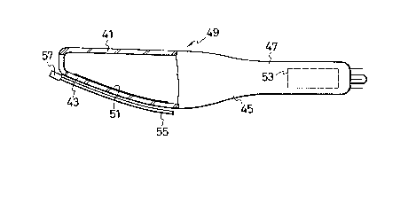
FIGS. 2 and 3 show an exam?le of the beam-index type
c310r cathode ray tube according to the present inventlon. There
is shown a rerlex type device having a rlat glass envelope ~9
which includes a f-ont panel po- lon 41, a screen panel
portion 43 facing the front panel portion 41, and a neck
~ortion 47 connected through a conic--1 'unnel por~ion 45 to both
the front panel portion 41 and the screen panel portion g3. The
front panel portion 41 is rectangular in shapc and permits
colored light to pass therethrough. The screen panel portion 43
is also shaped rectangularly and is curved slightly, and is
provided on its inner surface with a phosphor screen 51 of
rectangular configuration along the screen panel portion 43. The
phosphor screen 51 includes a plurality of color phosphor stripes
of three primary colors and a plurality of index phosphor
stripes. In the neck portion 47, an electron gun assembly 53 is
provided to produce an electron beam impinging on the phosphor
screen 51 from the side of the front panel portion 41 to scan the
same. Since the phosphor screen 51 is curved along the screen
panel portion 43, the incident angle of the electron beam is
prevented from having large variations at different locations
over the phosphor screen 51.
At the outside of the screen panel portion 43 there is a
luminescence receiving plate member 55 which faces and extends
along the outer surface of the screen panel portion 43. An index
fluorescence detector 57 containing a photosensitive device such
as a photodiode is attached to one end of the luminescence
receiving plate member 55. The luminescence receiving plate
member 5~ receives lumineacence emitted rom each or the index
_ /~L
1~67~
phosphor stripes .hrough the screen panel portion 43 and is
operative to proauce secondary index fluorescence which may be
detected by the pho.osensitive device contained in the index
fluorescence de_ector 57 in response to the index fluorescence
emitted from the index phosphor strlpes. This luminescence
receiving plate mem~er 55 may be formed, for example, of an
acrylic resin ln which specific phosphors seles.ed for their
abllity to absorb index fluorescence rro~ .he index phosphor
strlpes and emi~.ing secondary index fluorescence ar- dlspersed.
The index fluorescence det~ctor 57 produc~s an index
signal in response to the secondary inde~ fluorescence r^ceived
and causes the electron beam generated by the electron gun
assembly 53 to be modulated with a color video signal supplied to
tne electron gun assemDly 53 in response to momentary scanning
positions of the electron beala on the phosphor screen 51.
As shown in detail in FIG. 4, the phospnor screen 51 is
formed with a plurality of index phosphor stripes 59 located on
the inner surface of the screen panel portion 43 and extending
parallel to one another at regularly spaced intervals. A porous
inorganic layer 60 is affixed on the inner surface,of the screen
panel portion 43 and extends between each adjoining pair of index
phosphor stripes 59. A metallic reflecting layer 61 is provided
to cover the index phosphor stripes 59 and the porous inorganic
layer 60. A plurality of color phosphor stripes of the three
primary colors containing red phosphor stripes 63R, blue phosphor
stripes 63B and green phosphor stripes 63G are provided on the
metallic reflecting layer 61 in a predetermined arrangement. The
red phosphor stripes 63R, the blue phosphor stripes 63B and the
green phosphor stripes 63~ ext-nd parallel to one another along
eacn of the index phosphor stripes 5g at regularly spaced
intervals and e-ch adjoining pair OL the red pnosphor stri?es
63~, blue phosphor stripes 63B and green phosphor stripés 63G are
located bet~een two adjoining index phosphor stripes 59.
Each of ~he index phosphor s~ripes 59 is composed o. a
phospnor emitting fluorescent materlal with a peak at a ranse of
ultraviolet r~ys in i.s spectral characteristic and having a
short persist3n^e charac~eristic such, ror example, as Y2SiO~:Ce.
The porous inorganic layer 60 may be composed, for
exar..ple, of al~minum oxide having a particle si2e of about the
same magnitude as that of tbe phosphor particles of which the
index phosphor stripes Sg are made and formed with a thickness
substantially equal to that of the ndex phosphor stripes 59 so
that a flat plane is formed with the surface of each of tne index
phosphor stripes 59 and the surface of the porous inorganic layer
60. As shown in FIG. 4, a porous inorganic layer 60 may also be
provided at the outer fringe or peripheral portions of the
phosphor screen 61.
The metallic reflecting layer 61 is made of aiuminum and
has a thickness, for example, of 500 to 1000 A so ~hat the
electron beam from the electron gun assembly 53 penetrates the
metallic reflecting layer from the side of the color phosphor
stripes to the side of the index phosphor stripes 59. In the
example shown in FIG. 4, a metallic reflecting layer 61 is
provided also on the porous inorganic layer 60 disposed at the
outer fringe portion of the phosphor screen 51.
The red, blue and green phosphor stripes 63R, 63B, and
63G located on the metallic reflecting layer 61 produce red
fluorescence, blue fluorescence, and gre=n fluorescence when
imping3d by ~n electron beam rrom th3 el_ctron g~1n asâem.~ly 3.
7~
The phosphor screen 51 of the configura~ion previously
described can be formed in the foilowing manner. Pirst, a slu-ry
including 2 ~hotoresi?at such 2a a solution of polyvinyl alcohol
containlng a~monium dichromate and containing aluminum oxide
par.icies of a particle size o~ substantially the same magnitude
as those of the phosphor of which each or the index phosphor
stripes ia mcde ia applied to the inner surf se OL the scr-en
panel por.ion 3 to cover the same. The slurry on the inner
surface or the scr--n panel portion 43 ls exposed to ligh
through a pnotomask which masks portions or the slurry
corresponding to locations where the index phosphor stripes 59
are to be formed. The photoresist is then develo2ed and dried to
form a layer of dried aluminum oxide constituting the porous
inorganic layer 60 which i9 fixed on the inner surLace of the
screen panel portion 43 with portions thereof being e~posed to
the light. Next, a slurry of index phosphor containing a
photoresist added thereto is applied on the surface of the porous
inorganic layer 60 and partial areas of the inner surface of the
screen panel 43 where the porous inorganic layer 60 is not
present, to cover the same. The slurry of index p,hosphor on the
surface of the porous inorganic layer 60 and the partial areas of
the inner surface of the screen panel 43 is exposed to light
projected through the screen panel portion 43 with the porous
inorganic layer 60 serving as a photomask from the outside of the
screen panel portion 43. This photoresist is then developed and
dried to form the index phosphor stripes 59 which are fixed on
the partial areas of the inner surface of the screen panel
portion 43.
-17-
:
~26~j8a~
Fo710wing this, as shown in ~IG. 5, the surface of the
porous inorganic layer 60 and the s~7rface OL e-ch of the index
phosphor stripes 5g whicn together form a flat plane are covered
Wi7 h an intermediate thin layer 62 OL an organic substance such
as an acrylic resin which is provia=d for fill ing up minut~
r~cesses on both the surface or the porous lnorganic 1-7yer 60 and
the sur_ace of e7ch o- the index phosphor s.ripes 59 3 make the
SUrL~CCS smooth. A me allic r_-iecting layer 61 havlng 2 s~ooth
surf-ce iâ rormed on the intermediate thin layer 52 to co~er the
same, the reflecting layer beins ror~sd by ~eans of vacuum
evaporatlon of aluminum. Subsequently, a slurry OL red phosphor
containing photoresist is put on the metallic reflecting layer 61
to cover the same, and the slurry is exposed to light through a
suitably configured photomask, developed, and dried to form red
phosphor stripes 63R fixed to the metallic reflecting layer 61
with portions thereof being exposed to the light. Next, a slurry
of blue phosphor containing photoresist is put on the metallic
reflecting layer 61 to cover tbe same and the slurry of blue
phosphor on the metallic reflecting layer is exposed to light
through a suitable photomask, developed and dried ~o form the
blue phosphor stripes 63B which are positioned between each pair
of adjoining red phosphor stripes 63R on the metallic reflecting
layer 61. Then, a slurry of green phosphor containing
photoresist is put on the metallic reflecting layer 61 and the
slurry of phosphor is exposed to light through a suitably
apertured photomask. The photoresist is developed and dried to
form the green phosphor stripes 63G which are located between
each pair of red phosphor stripes 63R and the blue phosphor
-18-
i~67~
stripes 53i on the m2tallic re lecting layer 61 with portions
thereoL belng e;posed to the light.
After the phosphor screen 51 is formed in the manner
described, the intermedla,e thin laver 62 or organic substancê is
evaporated and expelled through the inde phosphor stripes 59 and
the porous inorganic layer 60 to the outslde of the phosphor
sc een 51 bv means of a he~lns process ~h^r-in the scr_en p2
porLions 43 on whish the phosphor scresn 51 has been formed i3
subject-d to a high ~smpera~ure thermal tre~-~.enr. The vapor
resulting from the evaporation of the intermediate thin layer 62
is not prevented from escape but diffuses through the index
phosphor stripes 59 and the porous inorganic layer 60 to the
outside of the phosphor screen 51 and thus the ~etallic
rerlecting layer 61 is prevented from being protruded to have
blisters. Since the intermediate thin layer 62 is evaporated and
dispelied, the metallic reflecting layer 61 is adhered directly
to both the surface of the index phosphor stripes 59 and the
surface of the porous inorganic layer 60 to have a minutely rough
surface corresponding to the minute recesses on the surface of
each of the index phosphor stripes 59 and the surf~ce of the
porous inorganic layer 60. The metallic reflecting layer 61
having such a minutely rough surface serves to reduce reflection
of light from the outside and colored light from each of the red,
blue and green phosphor stripes 63R, 63B and 63G on the porous
inorganic layer 60 disposed at the outer fringe portion of the
phosphor screen 51. Consequently, the harmful influence exerted
upon color images by the reflection of light from the outside and
colored light from each of the red, blue and green phosphor
stripes 63R, 63B and 63G is effectively diminished.
--19--
1~i76~34
In the embodiment of the present invent on thus far
described, when the phosp:hor scr~en 51 is scanr.ed by the electron
beam 'rom the electron gun assembly 53 the index phosphor
stripe 5g on which the elect on beam impinges through the
me.allic rerlecting l~yer 61 is exci'_d by the electron be~m to
e~it the index fluor-scence A portion of the index fluor_scence
emi.._d toward the screen panel portlon 43 passes dir-srly
through the screen panel por.ion ~3 to en.er into the
iwminescence receiving plate member ;5 and another por_ion of the
index fluorescence e~ittea to~ard the metal'ic reflecting
layer 61 is reflected at that layer and then passes througn the
screen panel portion ~3 to en.er into the l~minescence receiving
plate member 55 Accoraingly, the 1ndex fluorescence emitted
from each of the index phosphor stripes ~9 is received
efficiently in the luminescence receiving plate member 55 and
therefore a secondary index fluorescence sufficient in intensity
is produced in response to the index fluorescence from each OL
the index phosphor stripes 59 in the luminescence receiving plate
member 55 and directed to the photosensitive device contained in
the index fluorescence detector 57
There is accordingly produced an index signal with a
superior signal-to-noise ratio in response to the secondary index
fluorescence from the index fluorescence detector 57 Momentary
scanning positions of the electron beam on the phosphor screen
with relation to each of the red, blue and green phosphor stripes
63R, 63B and 63G are detected on the strength of the index
signal, and the electron bealn is subjected to modulation with the
color video signals supplied to the electron gun assembly in
-20-
~2~7~
response to the de~ected momentary scannins positions to impinge
on eacn or the red, blue and green phosphor stripes 63R, 53B and
63G
~ portion of each of the red, blue and green
fluor~scence~ emi.ted through the f~ont panel portion 41 passes
dlrectly thr3ugh he .~nt panel portion 41 t~ re cn the ou.side
of the rlat glass envelope 49, and another portion of each of the
red, blue and g~een fiuorescences _mitted t~ward the metallic
rerlecting layer 61 is refl-c_ed at the metallic reflecting
layer 61 and then passcs through the fron- panel portion 41 to
reach tAe outside OL the flat glass envelope 49. The red, ~lue
and green fluorescences reach the outside of the flat glass
envelope 49 so that the color images dispiayed on the phosphor
screen 51 are observed through the front panel portion 41. As
that occurs, the portion of each of the red, blue and green
fluorescences emitted toward the metallic reflecting layer 61
also contribute to display the color images on the phosphor
screen 51 in addition to the portion of each of the red, blue and
green fluorescences emitted toward the front panel portion 41.
This results in an improvement in the luminous efficiency of each
of the red, blue and green phosphor stripes 63R, 63B and 63G.
As the index fluorescence emitted from each of the index
phosphor stripes 59 is directed to the front panel portion 51
after passing through the metallic~reflecting layer 61 and
thereby weakened, each of the fluorescences reaching the outside
of the flat glass envelope 49 to be observed is prevented from
being deteriorated in color purity due to the index fluorescence.
Since the index fluorescence emitted from each of the
index phosphor stripes 59 is directed efficiently to the
-21-
~L267~;~4
luminescence r~seiving piate member 55 as mentioned above, the
electron beam for exciting each of the index phosphor stripes 53
c-n be decreased n density. In th2t case/ since a dark elo~t_on
béam current in the cathode ray tube is reduce,d the black lev~l
of tho color image on the pAos?hor screen 51 is prevented from
rising so the c~lor image on the phosphor screen 51 is improved
in quality.
FIG. 6 show another -mbodim_nt Oc the beam-index t~pe
color cathode ray tube of the pr-sent invention. In FI~. 6,
elements and portions correspondinq t3 those of FIG. 4 are
provided with the same reference numerals and therefore further
description or those elements will be omitted.
In this embodiment, a porous inorganic layer 60P is
provided in the phosphor screen 51 to correspond substantially to
the porous inorganic layer 60 shown in FIG. 4. The inorganic
layer 60P contains a pigment dispersed therein so as to provide a
predetermined color. The porous inorganic layer 60P is made, for
example, of aluminum oxide of a particle si2e of the same order
of magnitude as that of the phosphor particles which comprise the
index phosphor stripes 59 and a black inorganic pigment is
dispersed in the aluminum oxide. The thickness is substantially
equal to that of each of the index phosphor stripes 59 so that a
flat plane is formed with the surface of the index phosphor
stripes 59 and the surface of the porous inorganic layer 60P.
The black inorganic pigment may, for example, consist of titanium
monoxide (TiO~.
The phosphor screen 51 having the porous inorganic
layer 60P containing the black inorganic pigment dispersed
therein is formed in the following manner. First, a slurry
-22-
containing a photoresist such as an aqueous soiution of polyvinyl
alcohol containing a~monium dichromate is mixed with aluminum
oxide of a particle size of subst~ntizlly the same masnitude as
tha. of the phosphor of which the index phosphor stripes 53 are
made. A black incrganic pigment in an Gmount OL Gsout 30 to iO
weight percent is pu~ On the inner surCace of 2 screen panel
portion 43 to cover the sam_. The slurry on the inner surLac~ OL
the screen panel por~ion 43 Ls exposed to ligh~ through a
photomask which masks portions of the slur y corresponding to
locations where the index phosphor stripes 59 are to be formeà.
The photoresist is then developed and dried to form the porous
inorganic layer 60P which is fixed on the inner surface o- the
screen panel portion 43 with portions thereof being exposed to
the light. The porous inorganic layer 63 contains the black
inorganic pigment dispersed therein and therefore exhibits a
black color.
Next, as shown in FIG. 71 the index phosphor stripes 59,
an intermediate thin layer 62 of organic material, and a metallic
reflecting layer 61 are formed in the same manner as described in
connection with the example shown in FIG. 5.
Red, blue and green phosphor stripes 63R, 63B and 63G
are then formed on the metallic reflecting layer 61. In this
process, as shown in FIG. 7, a slurry of phosphor for the green
containing photoresist is put on the metallic reflecting layer 61
to form a green phosphor layer 39, which layer is exposed to
light Lp from a predetermined light source through a photomask 40
for green phosphor stripes. The light source for supplying the
light Lp comprises, for example, a mercury arc lamp having an
emission spectrum cnaracteristic in which radiation peaks Oc
~21~7~
large levei appear both within the ultra-7iolet range and the
visible light range as shown in FI&~ 8 where the orainates
represent the light level and the abscissae represent wavelengrh.
When the green pnosphor layer 39 on the metallic
re_lecting layer 61 is exposed to the light Lp pas3ins through
openings ao2 of the photomask gO, the condltion o_ exposur^ o~
the green pho_phor layer 39 to the light Lp is observed rom _..e
outside of the screen panel portion d3 and the position of the
photomask ao is adjusted so as to cause the light Lp having
passed through the openings 40a of the photomask 40 to re~ch
locations on the green phosphor layer 39 at which the green
phosphor stripes 63G are to be formed in predetermined relation
to the index phosphor stripes 59. Thus, positional adjustment
for locating the photomask 40 correctly for determining the
positions of the green phosphor stripes 63 is carried out. In
this situation, the light Lp entering the index phosphor
stripes S9 re~ches the outside of the screen panel portion 43
with relatively small attenuation while the light Lp entering
in the porous inorganic layer 60P is absorbed for the most part
by the bLack inorganic pigment dispersed in the la~er 60P and
therefore attenuated considerably in reaching the outside of the
screen panel portion 43. Accordingly, the light Lp observed at
the outs1de of the screen panel portion 40 has a relatively large
luminosity at locations corresponding to the index phosphor
stripes 59 and a small luminosity at locations corresponding to
the porous inorganic layer 60P.
In this way, it is possible to check whether the light
Lp having passed through the opening 40a of the photomask 40
enters in the locations corresponding to the index phosphor
-24-
~ 6~3~
stripes 59 or in locations corresponding to the porous inorganis
layer 60P by observing tne condltion of exposu-e o- the green
phosphor layer 33 from the outside of the screen panel 43 to
detQ-t the luminosi y of the light Lp. Further, as apparent from
FIG. 6, the position of the green phosphor st ipe 63G should be
adjacent to the position o the index phosphor stripQ 59 without
overla?ping. ~ccor~lngl~, the photomas' 40 shoul~ be locat-d S'J
as not to cause he light Lp having passed through the
openina 40a of .he photomask 40 to enter in location~ ont he
green phosphor layer 39 corresponding to the index phospho.
stripes 59. In other words, the photomask 40 should be located
so as to cause the light Lp observed at the outside of the screen
paneL portion 43 to have minimum luminosity all over the phosphor
screen 51.
The posi~ional adjustment of the photomask 40 for
locating the same so as to cause the light Lp observed at the
outside of the screen panel portion 43 to have minimum luminosity
over the entire phosphor screen 51 is carried out, for example,
as shown in FIG. 9.
First, the photomask 40 is located at a position
indicated by the dot-dash line in FIG. 9. Under these
conditions, some of the openings 40a of the photomask are placed
at positions corresponding to the index phosphor stripes 59 so
that the light having passed through the openings 40a of the
photomask placed at the positions corresponding to the index
phosphor stripes 59 enters in the index phosphor stripes 59 and
reaches the outside of the screen panel portion 43 with
relatively large lw~inosity as represented by a level Bh in
FIG. 9. Thus, the light Lp observed at the out-ide o} the screen
-25-
~L2~'76~
panel portion 43 has maximum luminosity ail over the phosphor
screQn 51.
Next, the photomask 40 is shifted in the direction
indicated by the arrow R in FIG. 9. W1th this snirt, the
1UminOSit J OL tne light L2 observed at the outside or the scrQQn
panel portion 43 is r3duced gradually. Then, the photomask 40 ls
loca.ed at a posi_ion indlcated wlth the solid llnQ in FIG. 9 so
that the lumino~ity OL- the li5ht Lp obs~rved at the outside or
the scrQen panel portion 43 becomes a min:imum all over the
phospnor screen 51. ~nder these conditions, each of the openings
aoa of the photomask 43 is placed at a position adjacent LO the
position or the index phosphor stri2e 59 wlthout overlapping so
a~ to cause the light Lp having passed through the openings 40a
of the photomask 40 to enter in location on the green phosphor
layer 39 where the stripes 63G are to be formed. The light Lp
entering in the locations on the green phosphor layer 39 at which
the green phospnor stripes 63G are to be formed reaches the
outside of the screen panel portion 43 with a small luminosity as
represented by a level Bl in FIG. 9.
Since the distance Dc between the center of the index
phosphor stripe 59 and the center of the green phosphor stripe
63G adjacent to the index phosphor stripe 59 is a predetermined
constant, the distance between the center of each of the
openings 40a of the photomask 40 placed at the positions
corresponding to the index phosphor stripes 59 and the center of
each of the openings 40a at the positions corresponding to the
locations on the green phosphor layer 39 at which the green
phosphor stripes 63G are to be formed is also equal to the
distance Dc. Accordingly, it is possible to loca.3 properly the
26-
photomask 40 so as to place the openings ~Oa at the positions
corr-spond ng t3 the locations on the green pAosphor layer 33 at
which the green phosphor stripes 63G are to be formed as shown by
the solid line in FIG. 9, by m^ans of shifting the photomask ~3
which is locatea such that some 0c the openings 40a are pl~ced ~t
the positions corresponding to the inde~ phosphor stripes 59,
indicated by the dot-dash line ln FlG. 9, by a distance
corresponding to 3c in the direction of the arrow R -hown in
FIG. 9.
After the photomask 40 ls correctly located through the
positional adjustment tnereof as mentioned above, the green
phosphor layer 39 is exposed to the lisht Lp p~ssing through the
openings 40a ror a predetermined period, then developed and dried
to form the green phosphor stripes 63G which are fixed on the
metallic reflecting layer 61, with portions exposed to the light.
In succession, the slurry for the red containing
photoresist is placed on the metallic refiecting layer 61 to form
a red phosphor layer and the red phosphor layer on the metallic
reflecting layer 61 is exposed to the light Lp through a
photomask for red phosphor stripes. At this time,.the positional
adjustment of the photomask for red phosphor stripes is carried
out in the same manner as the positional adjustment of the
photomask 40 for green phosphor stripes. Then the red phosphor
layer is exposed to light Lp passing through the photomask for
red phosphor stripes for a predetermined period, developed and
dried to form the red phosphor stripes 63R, which are Located
between each pair of adjoining green phosphor stripes 63G on the
metallic reflecting layer 61.
-27-
~;2 6'7~
The slurry of the blue phosphor is then put on the
metallic re~lecting layer 61 to form a blue phosphor layer which
is exposed to lignt Lp through a photomask for blue phosphor
st~ipes. The posi ional adjust~ent of the photomask for blue
pnosphor siripes is also ca~ried out as in the same manner
described for th- green phosphor stri~es. Then, the blue
phosphGr layer is e posed to light Lp passlng through the
photomask for blue phos?hor s.~ipes for a precet-rmined period,
then develoDed and dried to form the sl~ue phos?hor stripes o3B,
which are fixed between each pair of green phosphor stripes 63G
and the red phosphor stripes 63R on the metallic reflecting
layer 61.
After the green, red and blue phosphor stripes are
formed on the melallic reflecting layer 61 as described above,
the intermediate thln layer 62 is evaporated and dispelled
through the lndex phosphor stripes 59 and the porous inorganic
layer 60P in the same manner as in the example of FIG. 4.
~: :As apparent from the above description, in this
embodiment with the porous inorganic layer 60P containing a black
inorganic pigment dispersed therein, the green, re~ and blue
: phosphor stripes 63G, 63R and 63B are easily positioned properly
in predetermined relation to the index phosphor stripes 59
througn observation of the light Lp for the exposure of each of
the green, red and blue phosphor layers conducted through the
screen panel portion 43. The positional adjustment of each of
the respective photomasks is carried out in accordance with the
result of this observation in the process of ~orming the color
phosphor stripes on the metallic reflecting layer 61.
-2~-
~2~6~3~
In the example given, the porous inorganic layer 60P is
made of aluminum oxide and including a black inorganic pigment
dispersed therein. Other inorganic substances can also be used
for forming the porous inorganic layer 602, and a blue pigment, a
grPen pigment, a brown pigment, or the like, can be appiied
instead of the blac!c inorganic pigment.
FIG. 10 shows an essential part of anotner embodiment of
the beam-index type color cathode ray tube according to the
present invention. In FIG. 10, the elements and portions
corresponding to those of FIG. 4 are identified with the same
reference numerals and further description thereof will be
omitted.
In this embodiment, a metallic reflecting layer 61 is
provided to cover a plurality of index phosphor stripes 59 and a
porous inorganic layer 60 on a phosphor screen 51 is provided
with an oxidized surface 6LF. This surface may be obtained
~hrough a process of surface treatment with an oxidizing agentO
The oxidized surface 61F of the metallic reflecting layer 61 is
inactivated to have reduced bonding ability to portions other
than an insoluble hardened portion of the color ph~sphor so that
unnecessary color phosphor not used for forming the color
phosphor stripes can easily be eliminated from the metallic
reflecting layer 61 in the process of forming the color phosphor
stripes on the metallic reflecting layer 6L.
The phosphor screen 51 having the metallic reflecting
layer 61 and an oxidized surface 61F may be formed in the
following manner.
First, as shown in FIG. llA, the porous inorganic layer
60 and the index phosphor stripes 59 are fixed on the inner
~lEi76~3~
sur~acs of a screen panel portion 43 and the metallic reflecting
layer 61 is provided with an intermediate thin layer 62 or
organic substance on the porous inorganic layer 60 and the index
phosphor stripes 59 in the same manner as the example shown in
FIG. 5. The metallic rerlecling layer 61 may be formed by ~eans
of vacuum evaporation of al~minum.
Then, the meta'L c refle~tins iayer 61 is subjected to
surr~ce trea ment with an oxidizing asent ana is t;~ere~y provided
with an oxidized surface 61~ aS shown in FIG. llA. In the
sur,ace treatment, for ex~mple, an aqueous solution including
potassium permangânate in an amount of 0.0001 to 0.0002 weight
percent or an aqueous solution containing a~monium dichromate of
0.001 weight percent is used as the oxidizing agent. The
metallic rerlecting layer 61 is dipped in the aqueous solution
containing eithêr the potassium permanganate or a~monium
dichromate for about 30 seconds, washed in water, and dried.
Next, as shown in FIGo llB, for example, a slurry of
green phosphor containing a photoresist is put on the oxidized
surface 61~ of the metallic reflecting layer 61 to form a green
phosphor layer 39. This phosphor layer 39 on the pxidized
surface 61F of the metallic reflecting layer 61 is exposed to
light through a photomask 40 for green phosphor stripes as shown
in FIG. llC. As a result of the exposure of the green phosphor
layer 39, portions of the green phosphor layer 39 corresponding
to openings 40a of the photomask 40 are changed into insoluble
hardened portions~ The green phosphor layer 39 after exposure to
light is subjected to development and portions othêr than the
insoluble hardened portions of the green phosphor layer 39 are
dissolved in water to be eliminated so that a plurality of green
-30-
~L;~6~7~i;8~
phosphor stripes 63G are for~ed and arranged in accordance with
the openings 40a of tAe photomask 40 on the oxidl~ed s~rface 61F
of the metallic reflecting layer 61 with lnsoluble hardened
portions of .he sreen phosphor layer 39 as shown in FIG. llD.
Since the me,allic re lecting layer 61 is provided with
an oxldi~cd surf~ce 61~ which is inactivated so that it has
reduced bonding abilitY to the por.ions other than the insoluble
hardened portions of the green phosphor layer 33, such portions
are easily elimina-ed sufficiently from the oxidized surface 61F
of the r,etal1ic reflectlng layer in the process of de~elopment
utilizing normal developing time and normal developing pressure.
Then, in succession, a slurry of red phosphor is applied
to the oxidized surface 61F to form a red phosphor layer, and a
plurality of red phosphor stripes 63 are formed on the oxidized
surface 61F in the same way as the green phosphor stripes 63G.
They are disposed between adjoining two of the green phosphor
stripes 63G as shown in FIG. 10. Then a slurry of phosphor for
blue is put on the oxidized surface 61F of the metallic
reflecting layer 61 to form a blue phosphor layer and a plurality
of blue phosphor stripes 63B are formed on the oxidized
surface 61F in the same way. The blue phosphor stripes are
disposed between each pair of the green phosphor stripes 63G and
the red phosphor stripes 63R adjoining each other, as shown in
FIG. 10.
After the green, red and blue phosphor stripes are
formed on the oxidized surface 61F o~ the metallic reflecting
layer as mentioned above, the intermediate thin layer 62 is
evaporated and volatilized through the index phosphor stripes 59
and the porous inorganic layer 60 in the same manner as the
example or FIG. ~.
~l2~ 84
The described embodiments make use of aqueous solutions
contalning potassium permanganate or ammor.ium dichromate as
oxidizina agents in the surface treatment for the metallic
reflecting layer. Alternatively, an aqueous soiution including
perioaic acid (~IOa) or an aqueous solution lnsluding h~drogen
peroxide (~22) can be used.
It should be eviaent that va~ious modi-ications to the
described embodiments can be made wlthout d-?ar ing from the
scope or the novel concepts or the present inv~ntlon.
-32-