Note: Descriptions are shown in the official language in which they were submitted.
1~,'7'~
EL~CTRONIC CLOCK TUNING S~ST~M
BACKGROUND OF THE INVENTION
l. F eld of the Invention.
The present invention relates to clock
05 systems used in digital computers. In particular,
the present invention is an electronic clock tuning
system for tuning the delay of clock pulses
distributed throughout the computer.
2. Description of the Prior Art.
Msdern digital computers are formed by
hundreds of thousands and even millions of logic
elements. In computer architectures which are highly
integrated, these logic elements are fabricated on
very large-scale integrated (VLSI) circuit chips
known as gate arrays. The gate arrays themselves are
organized onto a plurality of ~ajor function circuit
boards which are dedicated to the performance of
specific tasks. A supercomputer, for example, can
include a central processing unit (CPU), memory
interface, and input/output (I/O) major function
circuit boards. Each of these circuit boards will
typically be formed by hundreds of gate arrays.
In order to achieve a high data throughput,
operations are distributed throughout the computer,
and performed in "parallel." Processed data and
microinstructions are communicated between individual
gate arrays, and between major function circuit
boards. It is extremely important, therefore, that
all microinstructions and data transfers executed by
the gate arrays be synchronized with those of other
gate arrays. To this end, the computer include~ a
central clock system for driving and or "clocking"
operations performed by all gate arrays.
0654N 23DEC86
The clock system will include a master
oscillator which is the source of clock signals for
all gate arrays. A clock pulse train produced by the
master oscillator is divided, and replicas thereof
05 distributed to each major function circui~ board by a
master fanout circuit. On each major function
circuit board the clock pulse train is further
divided, and distributed to each gate array through a
local fanout circuit. Each gate array is, therefore,
clocked by a replica of the pulse train produced by
the master oscillator. While this technique helps
maintain synchronization between gate arrays, it is
inadequate for the high degree of performance
demanded of modern supercomputers.
Even minute discrepancies between the phases
of the clock pulse trains arriving at different gate
arrays can have disastrous consequences on computer
operation. These discrepancies, or skews, are the
~ product of numerous factors. Variables such as
operating temperature, supply voltage, component
tolerance variables due to manufacturing processes,
and differing path lengths between master oscillator
and gate arrays, all contribute to skew between the
clock pulse trains. Adding to the proble~ is the
fact that many of these factors cannot be accurately
controlled.
Obviously, the higher the frequency of the
clock pulse train, the faster the computer can
process data. Frequency of the clock pulse train,
however, is limited by the uncertainty, or maximum
skew, introduced between clock pulse trains supplied
to various gate arrays. Simply put, computer
performance can be greatly increased by reducing
0654N 23DEC86
~ '(J(~
skews introduced by the clock system~
Currently used techniques for tuning
computer clock systems are primarily manual. A
technician will measure the time delay in the
05 distribution path between the master oscillator and
each and every gate array. ~ length of coaxial cable
in each path is then removed, trimmed, and
reinserted. This procedure is repeated until the
delay in the clock pulse train at each gate array is
wi.hin predetermined tolerances. This procedure is
obviously very labor intensive. It must be performed
for each and every one of the hundreds of gate arrays
on the computer. On a supercomputer, this procedure
can take several weeks.
15There is clearly a continuing need for
improved apparatus for tuning clock systems in
digital computers. An electronic clock tuning system
would be especially desirable. Electronic test
equipmant could then be used to tune the clock pulse
train supplied to each gate array. Computer "setup"
time could be greatly reduced by the elimination of
tedious and labor intensive tasks. An electronic
clock tuning system of this type could also be
extremely accurate, and significantly increase
computer performance by permitting gate arrays to be
clocked at frequencies approaching their specified
maximums. The system should, of course, also be
relatively simple and inexpensive.
SUMMARY OF THE INVENTION
The present invention is an electronic clock
tuning system for delaying a clock pulse train by one
of a plurality of discrete delay periods. The
electronic clock tuning system incl~des means for
0654N23DEC86
(3()
producing digital delay select signals representative
of the discrete delay periods, and means responsive
thereto for delaying the clock pulse train by
discrete delay periods represented by the delay
05 select signals. Use of this system permit~ clock
pulse trains distributed to individual gate arrays
throughout a computer to be tuned so as to have
identical phases or skews. This task can be quickly
performed by electronic test equipment, thereby
significantly reducing computer setup time and
expense. The extremely high degree of accuracy
obtainable through use of the system permits all gate
arrays to be clocked at frequencies approaching the
upper limits of their specifications, and still be
accurately synchronized with all other gate arrays
within the computer. As a result, the clock tuning
system is an important contribution to the
performance required for demanding supercomputer
applications.
In a preferred embodiment, the means for
producing the digital delay select signals includes a
coarse delay register and a fine delay register. The
coarse delay register is adapted to receive coarse
delay tuning codes, and produces coarse delay select
signals representative of one of a plurality of
discrete coarse delay periods. The fine delay
register is adapted to receive fine delay tuning
codes, and produces fine delay select signals
representative of one of a plurality of discrete fine
delay periods.
The means for delaying the clock pulse train
by discrete delay periods includes a fine delay
circuit, and a coarse delay circuit. The coarse
0654N 23DEC86
~ t3~)
delay circuit is responsive to the coarse delay
register, and includes a plurality of first delay
elements having an input connected to receive the
clock pulse train, and an output. Each coarse delay
OS element is adapted to delay the clock pulse train by
one of the plurality of discrete coarse delay
periods. The coarse delay circuit also includes a
multiple~er which has signal inputs connected to the
outputs of the first delay elements to receive the
delayed clock pulse trains, a signal output, and a
control input responsive to the coarse delay
register~ The multiplexer supplies to its signal
output one of the delayed clock pulse trains, as
represented by the coarse delay select signal.
The fine delay circuit is connected to
receive the coarse delayed clock pulse train from the
multiplexer, and further delays the clock pulse train
by one of a plurality of fine delay periods. The
fine delay circuit includes a transmission line to
which a plurality of binary weighted loads are
switchably interconnected by transmission gates. The
transmission gates are responsive to the fine delay
register, and the fine delay circuit further delays
the clock pulse train by one of a plurality of fine
delay periods, as represented by the fine delay
select signals.
In one preferred embodiment, the coarse
delay register is a four bit shift register, and the
coarse delay circuit means introduce one of sixteen
coarse delay periods which are int~ger multiples of
five hundred picoseconds. The fine delay shift
register is also a four bit shift register, and fine
delay circuit means further delays the clock pulse
0654N 23DEC86
~ 7'^~
traln by one of sixteen fine delay periods whlch are integer mul-
tiples of one hundred picoseconds. Clock pulse trains can
thereby be tuned to an accuracy of one hundred picoseconds.
Thus, according to one aspect thereof the present
invention provides an electronic clock turning system for dis-
tributing tuned clock pulse trains to integrated circuit arrays
of a digital computer in which the gate arrays are organized into
a plurality of regions on each of a plurality of ma~or function
circuit boards; including master oscillator means for producing a
clock pulse train; master fanout means operatively connected to
th~ master oscillator means for distributing the clock pulse
train to each major function circuit board; a plurality of local
fanout means, each mounted with respect to one of the ma;or func-
tion circuit boards and operatively connected to the master-fanout means for distributing the clock pulse train to each
region of the ma~or function circuit board; tuning code generator
means for generating coarse and fine digital delay tuning codes,
for each gate array, representative of desired discrete a plural-
ity of electronic delay means, each associated with an mountedwith respect to a region of ma;or function circuit board and
operatively connected to the local fanout means on the circuit
board, for distributing the clock pulse train to each gate array
of the region of the main ~unction circuit board with which it is
associated, and for delaying the distributed clock pulse train by
one of a plurality of discrete delay periods, each electronic
delay means comprising for each gate array of the region with
which it is associated; coarse delay select means coupled to the
tuning code generator means for producing digital coarse delay
select signals as a function of the coarse delay tuning codes;
fine delay select means coupled to the tuning code generator
means for producing digital fine delay select signals as a func-
tion of the fine delay tuning codes; coarse delay means coupled
to the coarse delay select means for delaying the clock pulse
train supplied to the gate array by discrete coarse delay periods
represented by the coarse delay select signals; and fine delay
-- 6 --
means coupled to the coarse delay means and the fine delay select
meaQs for delaying -the clock pulse train supplied to the gate
array by discrete fine delay pe~iods represented by the fine
delay select signals.
In one embodimen~ of this aspect of the pr~sent inven-
tion the electronic delay means further includes electronic delay
fanout means coupled to the local fanout means for distributing
the clock pulse train; and a plurality of coarse delay elements
having an input connected to receive a clock pulse train from the
electronic delay array fanout means, and an output, each coarse
delay element adapted to delay the received clock pulse train by
one of the discrete coarse delay periods; and the coarse delay
means includes a multiplexer having signal inputs connected to
the output of one of the delay elements, a signal output, and
control inputs responsive to the coarse delay select means, for
supplying at its signal output coarse delayed clock pulse trains
represented by the coarse delay select signals. Suitably the
coarse delay sel~ct means include coarse delay shift register
means for serially receiving the digital coarse delay tuning
codes and for producing the digital coarse delay select signals.
Desirably each of the coarse delay shift register means is a four
bit shift register which receives a four bit digital coarse delay
tuning code and produces a four bit digital coarse delay select
signal representative of one of sixteen discrete coarse delay
periods; each electronic delay array means includes sixteen
coarse delay elements, each delaying the clock pulse train by a
different coarse delay period; and each of the multiplexers is a
sixteen input multiplexer. Preferably each of the sixteen coarse
delay periods is a multiple of a five hundred picosecond period.
In another embodiment of this aspect of the present
invention the fine delay means include input means operatively
connected to the coarse delay means to receive the clock pulse
train, output means for outputting the delayed clock pulse train
from the fine delay means; transmission line means for transmit-
- ~a -
~ '7'~
tiny the ~elayed clock pulse train between the input means and
the output means; a plurality of load means for loading the
transmission line means and thereby delaying the clock pulse
train by the discrete delay periods; and a plurality of transmis-
sion gate means, each transmission gate means response to thefine delay select means for switchably interconnecting one of the
load means to the transmission line means in response to the dig-
ital fine delay select signals. Suitably the fine delay selec-t
means include shift reglster means for serially receiving digital
fine delay tuning codes and for producing digital fine delay
select signals. Desirably the load means of each fine delay
means are binary weighted. Suitably each of the fine delay shift
register means is a four bit shift register which receives a four
bit digital fine delay tuning code and produces a four bit digi-
tal fine delay select signal respresentative of one of sixteendiscrete fine delay periods; and each of the fine delay means
includes four transmission gate means and four load means, each
load means switchably interconnected to the transmission line
means by a transmission gate means, wherein each fine delay means
delays the clock pulse train by one of sixteen different fine
delay periods. Desirably each of the sixteen fine delay periods
is a multiple of a one hundred picosecond period.
In a still further embodiment of this aspect of the
present invention the tuning code generator means includes means
for generating coarse and fine digital delay tuning codes for
each gate array in a serial format; and the coarse delay select
means and the fine delay select means of each gate array are
connected in series with one another, and in series with the
coarse delay select means and the fine delay select means of all
other gate arrays of a region, to receive the digital delay
tuning codes in a serial format.
In another aspect thereof the present invention pro-
vides an electronic clock tuning system for distributing tune
clock pulse trains to integrated circuit gate arrays of a digital
- 6b -
~ ~t~
computer in whi.ch the yate arrays are organized into a plurality
of regions on a circuit board, including master oscillator means
for producing a clock pulse train; local fanout means mounted
with respect to the circuit board and operatlvely connected to
the master oscillator means for distributing the clock pulse
train to each region of the circuit board; tuning code generator
means for generating digital delay tuning codes, for each gate
array of a region in a serial format, the tuning codes represen-
tative of desired discrete delay periods of the clock pulse
trains distributed to the gate arrays of the region; and a plu-
rality of electronic delay means, each associated with and
mounted with respect to a region of the circuit board and opera-
tively connected to the local fanout means for distributing the
clock pulse train to each gate array of the region with which it
is associated, and for delaying the distributed clock pulse
trains by one of a plurality of discrete delay periods, each
electronic delay means comprising a plurallty of delay shift reg-
ister means, each associated with a gate array of the region, for
receiving the digital delay tuning codes and for producing digi-
tal delay select signals representative of discrete delay periodsin a parallel format, the delay shift register means for each
region all being connected in series with one another and in
series with the tuning code generator means; and a plurality of
delay means each associated with and coupled to receive the delay
select signal from one of the delay shift register means, for
delaying the clock pulse trains supplied to the gate array with
which it is associated by discrete delay periods represented by
the digital delay select signals. Suitably the tuning code gen-
erator means includes means for generating coarse and fine digi-
tal delay tuning codes, for each gate array, representative ofdesired discrete delay periods of the clock pulse trains dis-
tributed to the gate arrays; the delay shift register means asso-
ciated with each gate array includes coarse delay shift register
means for producing digital coarse delay select signals as a
3~ function of the coarse delay tuning codes; and fine delay shift
register means for producing digital fine delay select signals as
- 6c -
a function of the fine delay tuning codes, wherein the coarse
delay shift register means and fine delay shift register means
for each gate array are coupled in series with one another, and
in series with all other coarse delay shift register means and
fine delay shift register means; and the delay means associated
with each gate array include coarse delay means coupled to the
coarse delay shift register means for delaying the clock pulse
train supplied to the gate array by discrete coarse delay periods
represented by the coarse delay select signals; and fine delay
means coupled to the coarse delay means and to the fine delay
shift register means for delaying the clock pulse train supplied
to the gate array by discrete fine delay periods represented by
the fine delay select signals. Desirably the electronic delay
means further includes electronic delay fanout means coupled to
the local fanout means for distributing the clock pulse train;
and a plurality of coarse delay elements having an input con-
nected to receive a clock pulse t.rain from the electronic delay
array fanout means, and an output, each coarse delay element
adapted to delay the received clock pulse train by one of the
discrete coarse delay periods; and the coarse delay means
includes a multiplexer having signal inputs connected to the out-
put of one of the delay elements, a signal output, and control
inputs responsive to the coarse delay select means, for supplying
at its signal output coarse delayed clock pulse trains repre-
sented by the coarse delay select signals. Suitably the finedelay means include input means operatively connected to the
coarse delay means to receive the clock pulse train; output means
for outputting the delayed clock pulse train from the fine delay
means; transmission line means for transmitting the delayed clock
pulse train between the input means and the output means; a plu-
rality of load means for loading the transmission line means and
thereby delaying the clock pulse train by the discrete delay
periods; and a plurality of transmission gate means, each trans-
mission gate means response to the fine delay select means for
switchably interconnecting one of the load means to the transmis-
sion line means in response to the digital fine delay select sig-
- 6d -
nals.
The present invention will be further illustrated by
way of the accompanying drawings, in which:-
Figure 1 is a block diagram representation of a com-
puter which includes the electronic clock tunlng system of the
present invention;
Figure 2 is a block diagram representation of the elec-
tronic clock tuning system shown in Figure 1;
Figure 3 is a block diagram representation of an elec-
tronic delay array (EDA) shown in Figures 1 and 2; and
Figure 4 is a schematic representation of a fine delay
circuit element shown in Figure 3.
A computer 12 which includes electronic clock tuning
system 10 of the present invention is illustrated in block dia-
gram form in Figure 1. Computer 12 is highly integrated, and
formed by a plurality of ma~or function circuit boards 14A-14X
(only 14X is illustrated). Major function circuit boards 14 are
: sub-systems of computer 12, and are dedicated to performing spe-
cific operations. In one embodiment, computer 12 ls a high speed
supercomputer, which includes a central processing unit board, a
shared memory interface board, and an input~output interface
board.
Each ma;or function circuit board 14 is organized into
a plurality of smaller functional units or regions 16A-16X. In
one embodiment (not shown), ma~or function boards 14 can include
up to
- 6~ -
sixteen regions 16. Each region 16 is in turn
formed by a plurality of very large-scale integrated
(VLSI) circuit elements or gate arrays 18A-18X. Gate
arrays 18A-18X can also be characterized as ~ubsystem
05 components of major function boards 14A-14X. Logic
elements which perform digital operations are
fabricated onto gate arrays 18 during manufacture.
Clock tuning system 10, as shown in Figures
1 and 2, includes master oscillator 20, master fanout
circuit 22, a local fanout circuit 24 on each major
function board 14, and a plurality of electronic
delay arrays (EDA) 26A-26X, one of which is
associated with each region 16 of major function
board 14. As shown in Figures 2 and 3, a plurality
of first or coarse delay elements 56A-56X are
associated with each EDA 26A-26X. Delay elements
56A-56X are not shown in Figure 1 for reasons of
clarity.
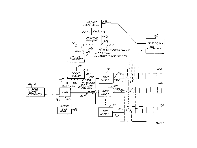
Operation of clock tuning system 10 is
perhaps best illustrated with reference to Figure 2.
Master oscillator 20 produces a source clock pulse
train 28 which is supplied to master fanout circuitry
22 by a trans~ission line such as coaxial cable 30.
As shown, clock pulse train 28 is comprised of a
plurality of rectangular pulses which switch between
first and second logic states (e.g. logic "O" and
logic "1" states) at a master frequency.
Master fanout circuit 22 is connected to
receive clock pulse train 28, and produces a
plurality of major function clock pulse trains
32A-32X. Clock pulse trains 32A-32X are replicas of
clock pulse train 28, and are distributed to one of
major function boards 14A-14X on transmission lines
0654N 23DEC86
'7'~ t
34A-34X, respectively.
On each major function board 14, (board 14X,
for example, as shown in Figures 1 and 2) major
function clock pulse train (32X in this example) i5
05 supplied to a local fanout circuit 24 by a
transmission line such as coaxial cable 36. Local
fanout circuit 24 divides clock pulse train 32 and
produces a plurality of EDA clock pulse trains
38A-38Xo EDA clock pulse trains 38A-38X are supplied
to electronic delay arrays 26A-26X by transmission
lines 40A-40X, respectively, as shown.
From each EDA 26A-26X, the EDA clock pulse
train 38 is again divided, and a plurality of tuned
clock pulse trains 42A-42X are produced. Each tuned
clock pulse train 42A-42X is a replica of EDA clock
pulse train 38, and, therefore, source clock pulse
train 28. A tuned clock pulse train 42A-42X is
supplied to each gate array 18A-18X, respectively, of
each region 16A-16X by a transmission line 44.
Having been propagated to the respective
gate arrays 18 through transmission lines 30, 34, -~6,
40, and 44, fanout circuits 22 and 24, and electronic
delay arrays 26A-26X, clock pulse trains 42A-42X will
have been delayed due to various factors. Different
delays will have been introduced to different clock
pulse trains 42A-42X. As a result, some of tuned
clock pulse trains 42A-42X will be out of phase, or
skewed, with respect to others. Clock pulse trains
42B and 42X, for example, as illustrated in Figure 2,
have arrived at gate arrays 18B and 18X,
respectively, with no phase difference or skew. As
illustrated, their rising edges R and trailing edges
T occur at identical times. Clock pulse train 42A,
0654N 23DEC86
$3~;~';1()()
however, has arrived at gate array 18A with a
different delay than that of clock pulse trains 42B
and 42X. As shown, rising edges R of clock pulse
train 42A are skewed with respect to those of clock
05 pulse trains 42B and 42X by a period S. As a result,
the operations ~eing performed by gate array 18A will
not be synchronized with those performed by gate
arrays 18B and 18X.
Through the use of electronic delay arrays
26A-26X, gate array clock pulse trains 42A-42X can
all be electronically tuned so as to have identical
delays when they arrive at a test point on their
respective gate array 18A-18X. Clock pulse trains
42A-42X will, therefore, have identical phases, and
no skew S. In this manner, all microinstruction
executions and data transfers of gate arrays 1~ can
be synchronized with those of all other gate arxays
18. Computer 12 can, therefore, ope-ate at higher
speeds, and achieve higher performance levels.
A preferred embodiment of electronic delay
array 26A (which is typical of EDA's 26A-26X) is
illustrated in Figure 3. Electronic delay array 26A
has an input terminal 50 connected to receive an EDA
clock pulse train 38A from local fanout circuit 24.
EDA 26A includes an EDA fanout 51 which is connected
to input terminal 50. EDA fanout 51 divides, and
produces a plurality of replicas of EDA clock pulse
train 38A, for distribution to delay elements 56A-56X
through terminals 53A-53X. Digital tuning codes,
preferably in serial format, are received by EDA 26A
on tuning code input terminal 52. Tuned gate array
clock pulse trains 42A-42X are supplied to gate
arrays 18A-18X through pins 54A-54X, respectively.
065~N 23DEC86
t)
-- 10 --
Associated with ~DA 26A are a plurality of
discrete delay elements 56A-56X. Delay elements
56A-56X are preferably external to EDA 26A. Each
delay element 56A-56X, respectively, has an input
05 terminal 55A-55X connected to terminals 53A-53X,
respectively, of EDA fanout 51, and an output
terminal 57A-57X. Each delay element 56A-56X delays
EDA clock pulse train 38A by one of a plurality of
first, or coarse, delay periods. In one preferred
embodiment, EDA 26A includes sixteen delay elements
56A-56X, each of which delays the EDA clock pulse
train 38A by an integer multiple of five hundred
picoseconds. Delay element 56A, for example, delays
the received clock pulse train by five hundred
picoseconds, while delay element 56B delays the
received clock pulse train by one thousand
picoseconds, and so on. Although delay elements
56A-56X can take other forms, in one preferred
embodiment they are dif~erent lengths of printed
circuit delay line which closely approximate the
desired coarse delay periods.
EDA 26A also includes coarse delay
multiplexers 58A-58X, first or coarse delay (C.D.)
shift registers 60A-60X, second or fine delay
circuits 62A-62X, and second or fine delay (F.D.)
shift registers 64A-64X. Together, each coarse delay
multiplexer 58A-58X and delay elements 56A-56X form a
coarse delay circuit. Each coarse delay multiplexer
58A-58X, coarse delay shift register 60A-60X, fine
delay circuit 62A-62X, and fine delay shift register
64A-64X is associated with one of gate arrays 18A-18
for which EDA 26X produces a tuned clock pulse train
0654N 23DEC86
'[~ ;J(~(~
42A-42X, respectively.
Coarse and fine delay shift registers
60A-60X and 64A-64X, respectively, are preferably all
connected in a series arrangement for the serial
05 transfer of delay tuning codes received on tuning
code input pin 52. In the embodiment shown, all
shift registers 60A-60X and 64A-64X are four bit
shif~ registers. Coarse delay shift registers
60A-60X serially receive, and store, coarse delay
tuning codes, and produce a four bit coarse delay
select signal representative of one of sixteen
discrete coarse delay periods on busses 61A-61X,
respectively. Similarly, each fine delay shift
register 64A-64X serially receives, and stores, a
fine delay tuning code representative of one of
sixteen discrete fine delay periods, and produces
four bit fine delay select signals representative
thereof on busses 65A-65X, respectively.
In the embodiment shown, each coarse delay
multiplexer 58A-58X is a sixteen input multiplexer,
and has input terminals A-X connected to output
terminals 57A-57X of delay elements 56A-56X,
respectively. Each coarse delay multiplexer 58A-58X
also has a four bit control terminal connected to bus
61A-61X, respectively, to receive the four bit coarse
delay select signal from its respective coarse delay
shift register 60A-60X. In response to the
particular coarse delay select signal received at its
control terminal, coarse delay multiplexers 58A-58X
will supply to their output terminal 70 one of the
sixteen coarse delayed clock pulse trains from signal
input terminals A-X. In this manner, each coarse
delay multiplexer 58A-58X delays EDA clock pulse
0654N 23DEC86
1.~,1~ q' ~
- 12 -
train 38A hy one of sixteen discrete coarse delay
periods.
Fine dela~ circuit elements 62A-62X have
input terminals 67A-67X, respectively, connected to
05 receive the coarse delayed EDA clock pulse train from
coarse delay multiplexers 58A-58X, respectively, and
an output terminal 63A-63X. A four bit control
terminal of each fine delay circuit element 62A-62X
is connected to bus 65A-65X, respectively, to receive
the four bit fine delay select signal from its
respective fine delay shift register 64A-64X. In
response to the fine delay select signal, fine delay
circuit elements 62A-62X further delay the coarse
delayed EDA clock pulse train by one of sixteen
discrete fine delay periods. These further delayed
EDA clock pulse trains are output pins 54A-S4X,
respectively, as tuned clock pulse trains 42A-42X.
A preferred embodiment of fine delay circuit
element 62A (which is typical of elements 62A-62X) is
illustrated in Figure 4. Input terminal 67A and
output terminal 63A are interconnected by a
transmission line 72 which includes a plurality of
inverters 74A-74~ connected in a series arrangement.
Four load elements 76A-76D are adapted to be
interconnected to transmission line 72 by electronic
transmission gates 78A-78D, respectively. Each
transmission gate 78A-78D has a first terminal A
connected to transmission line 72, a second terminal
B connected to its respective load element 76A-76D,
and a control terminal C connected to one of control
terminal pins 79A-79D. Control terminal C of each
transmission gate 78A-78D, therefore, receives from
bus 65A one bit of the fine delay select signal
0654N 23DEC86
- 13 -
produced by the fine delay shift register 64A to
which it is attached. Each load element 76A-76D is
connected between a power supply potential (not
shown~, ground 80, and terminal B of its respective
05 transmission gate 78A-78D.
Although schematically represented as
switches in Figure 4, transmission gates 78A-78D are
electronic transmission gates fabricated on EDA 26A.
When a first (e.g. a logic "0" state) signal is
received at their control terminals C, transmission
gates 78A-78D are in their OPEN conduction state,
electrically disconnecting load elements 76A-76D from
transmission line 72. When the particular bit of a
fine delay select signal has a second (e.g. a logic
"1") state, the corresponding transmission gate
78A-78D will be in a CLOSED conduction state, and
electrically connect its load element 76A-76D to
transmission line 72. When one of load elements
76A-76D is connected to transmission line 72, it
loads transmission line 72 and thereby further delays
propagation of the EDA clock pulse train therethrough.
In a preferred embodiment, load elements
76A-76D are formed by MOS transistors in a manner
well known to those skilled in the art. Load
elements 76A-76B are also binary weighted so that one
of sixteen discrete fine delay periods can be added
to the clock pulse train. Gate load 76A preferably
has a binary weight of eight, and will further delay
the clock pulse train by eight hundred picoseconds
when interconnected to transmission line 72
transmission gate 78A. Gate load 76B has a binar~
weight of four, and will delay the clock pulse train
by four hundred picoseconds. Gate load 76C has a
0654N 23DEC86
1~1, .' ;'()(~
binary wei~ht of -two, and will further delay -the clock pulse
train by two hundred picoseconds. Gate load 76D has a binary
weight of one, and will further delay the clock pulse train by
one hundred picoseconds when interconnected to transmission line
72 by transmission gate 78D. The fine delay select signals pro-
duced by fin~ delay shift registers 64 can, therefore, digitally
represent one of sixteen fine delay periods, each of which is an
integer multiple of one hundred picoseconds~
A preferred method of uslng clock tuning system 10 is
u illustra~ed in Figure 2. Gate arrays 18A-18X preferably lnclude
a build-in self-test system havlng a test data output pln 80A-
80X, respectively. from which a copy of the tuned clock pulse
train can be monitored. Since the clock pulse train is propa-
gated through portions of gate arrays 18A-18X, delays dependent
upon the particular fabrication batch can be compensated for.
Electronic test,instrument 82 is used to measure the delay intro-
duced to the clock pulse train between master oscillator 20 and
test data output pin 80A-80X of each gate array 18A-18X. Delay
tuning code generator 84 then produces tuning codes which are
applied to tuning code input pin 52 so as to tune the tuned clock
pulse train 42 until a predetermined time delay is established.
In this manner, all gate arrays 18A-18X of all ma~or functions 14
can be tuned so as to have identically delayed clock pulse trains
42. This procedure can be automated, and quickly performed.
.
:
.
- 14 -