Language selection

Search

Patent 1267705 Summary

Third-party information liability

Some of the information on this Web page has been provided by external sources. The Government of Canada is not responsible for the accuracy, reliability or currency of the information supplied by external sources. Users wishing to rely upon this information should consult directly with the source of the information. Content provided by external sources is not subject to official languages, privacy and accessibility requirements.

Claims and Abstract availability

Any discrepancies in the text and image of the Claims and Abstract are due to differing posting times. Text of the Claims and Abstract are posted:

  • At the time the application is open to public inspection;
  • At the time of issue of the patent (grant).
(12) Patent: (11) CA 1267705
(21) Application Number: 1267705
(54) English Title: SEGMENTED CAPACITOR
(54) French Title: CONDENSATEUR SEGMENTE
Status: Expired and beyond the Period of Reversal
Bibliographic Data
(51) International Patent Classification (IPC):
  • H01G 02/14 (2006.01)
(72) Inventors :
  • MACDOUGALL, FREDERICK W. (United States of America)
  • MURPHY, THOMAS A. (United States of America)
(73) Owners :
  • AEROVOX INCORPORATED
(71) Applicants :
  • AEROVOX INCORPORATED (United States of America)
(74) Agent: SMART & BIGGAR LP
(74) Associate agent:
(45) Issued: 1990-04-10
(22) Filed Date: 1987-05-27
Availability of licence: N/A
Dedicated to the Public: N/A
(25) Language of filing: English

Patent Cooperation Treaty (PCT): No

(30) Application Priority Data:
Application No. Country/Territory Date
868,295 (United States of America) 1986-05-28

Abstracts

English Abstract


Segmented Capacitor
Abstract of the Disclosure
A capacitor in which at least one of two
dielectrically-insulated metal layers is interrupted
along its length by a plurality of transverse
non-conductive gaps extending partway across the layer,
thereby dividing the layer into a series of conductive
sections each conductive section being connected to an
adjacent section by a narrow metallized region that
extends between the associated gap and one edge of the
layer; the narrow metallized regions is adapted to act
as a fuse for the section during periods of excessive
current flow to the section,


Claims

Note: Claims are shown in the official language in which they were submitted.


- 7 -
What is claimed is:
Claims
1. A capacitor comprising:
a dielectric strip,
first and second metal layers insulated from
one another by said dielectric strip,
each of said layers being interrupted along its
length by a plurality of transverse non-conductive gaps
extending partway across said layer,
said gaps dividing each said layer into a
series of conductive sections, each section being
connected to an adjacent section by a narrow metallized
region extending from the associated said gap to one
edge of said layer, said narrow metallized region being
adapted to act as a first fuse for said section during
periods of excessive current flow to said section and
wherein
the sections of each said layer are all
electrically connected in common along one edge of said
layer.
2. The capacitor of claim 1 wherein said
section extends to said edge and has an extent along the
lengthwise direction of said layer greater than the
widthwise extent of said narrow metallized region.
3. A capacitor comprising:
a dielectric strip,
first and second metal layers insulated from one
another by said dielectric strip,
at least one of said layers being interrupted
along its length by a plurality of transverse non-
conductive gaps extending partway across said layer,

- 8 -
said gaps dividing said layer into a series of
conductive sections, each section being connected to an
adjacent section by a narrow metallized region extending
between the associated said gap and one edge of said
layer, said narrow metallized region being adapted to
act as a first fuse for said section during periods of
excessive current flow to said section, and wherein
said gaps extend to the opposite edge of said
layer, and
said section is connected to the two adjacent
sections located on either side of said section,
respectively by two said narrow metallized regions
adapted to act as parallel fuses which must both fuse in
order to electrically isolate said section from said
adjacent sections.
4. A capacitor comprising:
a dielectric strip,
first and second metal layers insulated from one
another by said dielectric strip,
at least one of said layers being interrupted
along its length by a plurality of transverse
non-conductive gaps extending partway across said layer,
said gaps dividing said layer into a series of
conductive sections, each section being connected to an
adjacent section by a narrow metallized region extending
between the associated said gap and one edge of said
layer, said narrow metallized region being adapted to
act as a first fuse for said section during periods of
excessive current flow to said section, and wherein
said gaps do not extend to the other edge of
said layer, and

- 10 - 412-1639
10. The capacitor of claim 1, 3 or 4 wherein said layer
is patterned to form said gaps.
11. The capacitor of claim 1 wherein said second metal
layer comprises a corresponding arrangement of sections and gaps.
12. The capacitor of claim 11 wherein, said first and
second metal layers are oriented so that
at one end of said capacitor one edge of the first
layer is exposed while one edge of the second layer is inset
so as not to be exposed, and
at the other end of said capacitor, the other edge
of said second layer is exposed while the other edge of said
first layer is inset, and
conductive material is applied to said capacitor
ends for making electrical contact to said exposed edges.
13. The capacitor of claim 7, 8 or 9 wherein said cut
extends fully to one end of said roll but stops sufficiently
short of other end to provide said narrow metallized regions
along one edge of each of said layers.
14. The capacitor of claim 7, 8 or 9 wherein said cut
stops sufficiently short of both ends of said roll to provide
said narrow materialized regions along both edges of both
said layers.

- 10 - 412-1639
10. The capacitor of claim 1, 3 or 4 wherein said layer
is patterned to farm said gaps.
11. The capacitor of claim 1 wherein said second metal
layer comprises a corresponding arrangement of sections and gaps.
12. The capacitor of claim 11 wherein, said first and
second metal layers are oriented so that
at one end of said capacitor one edge of the first
layer is exposed while one edge of the second layer is inset
so as not to be exposed, and
at the other end of said capacitor, the other edge
of said second layer is exposed while the other edge of said
first layer is inset, and
conductive material is applied to said capacitor
ends for making electrical contact to said exposed edges.
13. The capacitor of claim 7, 8 or 9 wherein said cut
extends fully to one end of said roll but stops sufficiently
short of other end to provide said narrow metallized regions
along one edge of each of said layers.
14. The capacitor of claim 7, 8 or 9 wherein said cut
stops sufficiently short of both ends of said roll to provide
said narrow materialized regions along both edges of both
said layers.

- 11- 412-1639
15. The capacitor of claim 1 wherein said narrow
metallized region forming said first fuse is from 1 to 30
of the width of said layer.
16. The capacitor of claim 3 wherein said second metal
layer comprises a corresponding arrangement of sections and
gaps.
17. The capacitor of claim 4 wherein said second metal
layer comprises a corresponding arrangement of sections and
gaps.
18. The capacitor of claim 16 ox 17 wherein, said
first and second metal layers are oriented so that
at one end of said capacitor one edge of the first
layer is exposed while one edge of the second layer is inset
so as not to be exposed, and
at the other end of said capacitor, the other edge
of said second layer is exposed while the other edge of said
first layer is inset, and
conductive material is applied to said capacitor ends
for making electrical contact to said exposed edges.

Description

Note: Descriptions are shown in the official language in which they were submitted.


1~26770S
-- 1 --
Seqmented Capacitor
Bac~qround of the Invention
This invention relates to capacitors,
especially wound metallized film capacitors.
The dielectic separating the charged layers of
a wound capacitor deteriorates with use, finally
breaking down completely, resulting in a localized short
and consequent increases in local current density. This
condition may lead to catastrophic failure in which the
capacitor bursts or catches fire.
To prevent such failures, it is known to
incorporate within the capacitor a fusing portion which
responds to increases in local current density by
disconnecting the failed section of metallized film
prior to catastrophic failure.
SummarY of the Invention
A general feature of the invention is a
capacitor in which at least one of two
dielectrically-insulated metal layers is interrupted
along its length by a plurality of transverse
non-conductive gaps extending partway across the layer,
thereby dividing the layer into a series of conductive
sections each conductive section being connected to an
adjacent section by a narrow metallized region that
extends between the associated gap and one edge of the
layer; the narrow metallized region is adapted to act as
a fuse for the section during periods of excessive
current flow to the section.
Preferred embodiments of the invention include
the following features. The conductive section extends
to the edge of the layer and has an extent along the
lengthwise direction of the layer that is greater than
the widthwise extent of the narrow metallized region.
,~

12t~77(~S
In some embodiments, the gaps extend to the opposite
edge of the layer and the conductive section is
connected to the two adjacent sections respectively by
two narrow metallized regions that act as parallel fuses
that must both fuse in order to electrically isolate the
section from the adjacent sections. In other
embodiments, the gaps do not extend to the other edge of
the layer, so that the section is also connected to an
adjacent section by a second narrow metallized region
extending between the gap and that other edge, with the
second narrow region acting as a second parallel fuse.
A conductive material (e.g., endspray), applied along
the edge, acts as an additional parallel fuse along a
length of the edge that corresponds to the section. A
margin extends along the length of the layer between the
edge and the ends of the gaps and the margin is
uninterrupted. In some embodiments, the capacitor is
wound as a roll with the gaps formed by a cut passing
through the roll. In some embodiments, the layer is
patterned to form the gaps. The second metal layer has
a corresponding arrangement of sections and gaps. The
two layers are oriented so that at one end of the
capacitor, one edge of the first layer is exposed while
one edge of the second layer is inset so as not to be
exposed, and at the other end of the capacitor, the
other edge of the second layer is exposed while the
other edge of the first layer is inset; conductive
material is applied to the capacitor ends for making
eletrical contact to the exposed edges. In the cut
embodiments, the cut may extend fully to one end of the
roll but stop sufficiently short of the other end to
provide the narrow metallized regions along one edge of
both layers; alternately the cut may stop sufficiently
short of both ends of the roll to provide the narrow

12~;77~5
metallized regions along both edges of both layers. The
narrow metallized region is from 1 to 30% of the width
of the layer.
As advantages of the invention, effective
fusing is provided inexpensively and internally to the
capacitor, and the tendency of premature disconnection
is reduced, particularly when fusing is provided both by
the conductive end coating and by the narrow metallized
regions.
Other features and advantages of the invention
will be apparent from the following description of the
preferred embodiment, and from the claims.
Description of the Preferred Embodiment
We first briefly describe the drawings.
Drawinqs
Fig. l-is a perspective view of a preferred
embodiment.
Fig. 2 is a cross-sectional view at 2-2 in Fig.
1.
Fig.,3 is a perspective view, partially
unrolled.
Fig. 4 is an enlarged diagrammatic view of a
portion of Fig. 2.
Fig. 5 is an exploded view of a short length of
the two metallized dielectric strips of Fig. 3.
Fig. 6 is an exploded view of another
embodiment.
Structure, Manufacture, and Use
Referring to Figs. 1 and 3, capacitor 10 is
formed by winding two metallized dielectric strips 6, 8,
which form the electrodes, around a nonconducting core
12 made from an injection-molded thermoplastic. Strips
6, 8 (25-125 mm wide) overlap except for a lateral
offset L (preferably 0.5 to 2 mm). Each comprises

lZ67~
-- 4 --
metallized film consisting of a polypropylene substrate
14 on which a thin (preferably 100 500 Angstroms)
aluminum layer 16 is deposited (e.g., as supplied by
Steiner Film). A metal-free margin 18 (preferably 0.5
to 5 mm wide) is provided along one edge of each strip.
Strips 6, 8 are oriented during winding so that their
metal-free margins are on opposite ends 20, 22 of the
wound capacitor. Ends 20, 22 are flame or arc sprayed
with vaporized zinc 24 (or tin/zinc, tinJlead, or
aluminum) to a thickness of preferably 0.010" to 0.030"
to provide electrical contact with the electrodes.
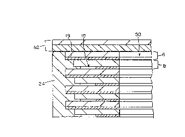
Referring to Figs. 1 and 4, end-spray 24
contacts the metallized margin 19 of electrode strip 6,
but only the metal-free margin 18 of electrode strip 8.
Connector tabs 26 are lead soldered or welded to
end-spray regions 24, for making electrical connections
to the capacitor.
Referring to Figs. 2 and 5, an end-milled
radial cut 28, oriented transversely to electrode strips
6, 8, penetrates capacitor windings 20 from outer
surface 29 to core 12. The cut does not extend far
enough in the transverse direction to sever either
metal-free margin 18, and leaves intact adjacent each
metal-free margin 18 narrow regions 30 of metallization,
and adjacent the other edges 21 of the metal layers of
strips 6, 8, narrow regions 32 of metallization. Cut 28
produces gaps 29 on the metal layers of strips 6, 8.
Because current flowing around a gap 29 through regions
30, 32 has an increased current density, the length of a
gap 29 and the resulting sizes of regions 30, 32 become
instrumental in selecting desired current densities, and
hence fusing capabilities, of regions 30, 32. The
length of a gap 29 is adjusted so that the width w of
region 30 (extending from margin 18 to the end of gap

12~77~5
29) on both electrodes is, e.g., 5% of the total
metallized width t. The width x of region 32 is greater
than w. Gaps 29 define a series of metallized sections
40. Each section 40 extends to edge 21 and is connected
to the two adjacent sections 40 by regions 30, 32.
Referring to Fig. 2, cut 28 is packed with
nonconductive, air-impermeable material 50, e.g., a
wax-like blend of polybutene and polythylene or
polyurethane resin, and capacitor 10 is encased by a
protective air-impermeable material 52, e.g., plastic
heat-shrink tubing, a plastic or metal canister, or
epoxy resin.
In use, capacitor 10 is connected to an
electric circuit via connector tabs 26. Regions 30, 32
provide conductive current pathways allowing the
capacitor to continue functioning in the event that
endspray contact at edge 21 is lost in the region of one
of the sections 40 as the result of a localized internal
short on that section. If the short heals itself, as
often occurs with metallized film, no further fusing
action will occur. If, however, the short does not
heal, the continued high current flow will vaporize
first regions 30 and then regions 32. Once all four
regions 30, 32 associated with a section 40 on one of
the layers 6 or 8 have vaporized the section 40 where
the short occurred will be isolated, while permitting
the remainder of the capacitor to continue to operate.
Thus the end-spray connection and the four fusing
regions can be seen as connected in parallel.
Other embodiments are within the following
claims. For example, capacitor 10 can be wound without
a core 12; a wound capacitor with or without a core can
be pressed into an oval profile; cut 28 may extend
beyond one, but not both metallized margins as shown in

~12~i77~
-- 6 --
Fig. 6; cut 28 may be produced using a circular saw,
milling machine, bandsaw, or a laser; the width of
fusible regions 30, 32 is preferably 1% to 30% of the
total metallized width; and the metallized coating may
be evaporated in a pattern to define gaps 29, rather
than cutting the capacitor after it is rolled.

Representative Drawing
A single figure which represents the drawing illustrating the invention.
Administrative Status

2024-08-01:As part of the Next Generation Patents (NGP) transition, the Canadian Patents Database (CPD) now contains a more detailed Event History, which replicates the Event Log of our new back-office solution.

Please note that "Inactive:" events refers to events no longer in use in our new back-office solution.

For a clearer understanding of the status of the application/patent presented on this page, the site Disclaimer , as well as the definitions for Patent , Event History , Maintenance Fee  and Payment History  should be consulted.

Event History

Description Date
Inactive: IPC deactivated 2016-01-16
Inactive: IPC assigned 2015-11-04
Inactive: First IPC assigned 2015-11-04
Inactive: Adhoc Request Documented 1994-04-10
Time Limit for Reversal Expired 1993-10-11
Letter Sent 1993-04-12
Grant by Issuance 1990-04-10

Abandonment History

There is no abandonment history.

Owners on Record

Note: Records showing the ownership history in alphabetical order.

Current Owners on Record
AEROVOX INCORPORATED
Past Owners on Record
FREDERICK W. MACDOUGALL
THOMAS A. MURPHY
Past Owners that do not appear in the "Owners on Record" listing will appear in other documentation within the application.
Documents

To view selected files, please enter reCAPTCHA code :


To view images, click a link in the Document Description column (Temporarily unavailable). To download the documents, select one or more checkboxes in the first column and then click the "Download Selected in PDF format (Zip Archive)" or the "Download Selected as Single PDF" button.

List of published and non-published patent-specific documents on the CPD .

If you have any difficulty accessing content, you can call the Client Service Centre at 1-866-997-1936 or send them an e-mail at CIPO Client Service Centre.

({010=All Documents, 020=As Filed, 030=As Open to Public Inspection, 040=At Issuance, 050=Examination, 060=Incoming Correspondence, 070=Miscellaneous, 080=Outgoing Correspondence, 090=Payment})


Document
Description 
Date
(yyyy-mm-dd) 
Number of pages   Size of Image (KB) 
Claims 1993-10-06 5 136
Drawings 1993-10-06 2 44
Abstract 1993-10-06 1 15
Descriptions 1993-10-06 6 195
Representative drawing 2001-05-14 1 10
Fees 1992-03-16 1 20