Note: Descriptions are shown in the official language in which they were submitted.
1~6~30~
IMPROVED OPTICAL FLOW SENSOR
BACKGROUND OF THE INVENTION
FIELD OF THE INVENTION
The present invention relates generally to appa-
ratus for sensing the flow of a fluid, and more particu~
larly to apparatus for detecting and measuring, by optical
means, the flow of a fluid that flows slowly enough for
individual drops to be detectedO
THE PRIOR ART
A fluid flow sensor that can detect and measure
the flow of individual drops of a fluid has many applica-
tions. A primary application for such a sensor is measur-
ing the flo~l of fluid through a drip chamber assembly in
an intravenous (nIVi') fluid infusion system. Such an IV
fluid infusion system generally includes a bottle contain
ing a fluid to be administered; a drip chamber assembly; a
tube connecting the bottle to an inlet at the top of the
drip chamber; a valve, associated with the tube, to control
the rate of flow of the fluid; a second tube connected to an
outlet at th~ bottom of the drip chamber; and injecting
means such as a hyp~dermic needle or catheter connected to
.. :
,
':`` ' ' '' ` '`` ~ ~ '' ~ ~ -
- ~ :
. .
.. : ... .
- , , , :. .
~268~)5~3
the second tube through which the fluid passes into the
patient.
A drip chamber assembly is usually cylindrical in
shape and has transparent walls enclosing a drip chamber.
The fluid enters the assembly through a drop former at the
top of the chamber and falls, one drop at a time, through
the chamber. The flow of the fluid through the chamber
can be monitored by visually observing the falling drops,
but various kinds of flow sensors have been developed to
detect the fall of these drops automatically and thereby
free the human observer for other tasks.
Examples of fluid flow sensors that can monitor
the flow of fluid through a drip chamber assembly are dis-
closed in U. S. Patent 3,596,515, issued to Cramer on
August 3, 1971, and U. S. Patent 4~397,648, issued to
Knute on August 9, 1983, both assigned to the assignee of
the present application. A flow sensor of the kind dis-
closed in these patents generally employs an optical ener-
gy emitter on one side of the drip chamber assembly and an
optical energy detector on the other side. The energy
emitter usually emits optical energy in the infrared or
visible light spectra (wavelength between about 300 nano-
meters and 2 microns). This optical energy passes through
- the transparent walls of the drip chamber assembly and
then strikes the detector. As each individual drop falls
: "-,
:
~" ;~ "~ ~" ,~ "
~i8053
through the chamber, it interrupts the flow of optical
energy, causins the detector to produce a corresponding
output signal. This output signal is then applied to a
monitoring device for further processing. The monitoring
device typically either sounds an alarm if the fluid stops
flowing or monitors the rate of flow of the fluid.
Existing flow sensors such as those disclosed in
the cited patents have certain shortcomings. One of these
is the need accurately to align the energy emitter and de-
tector during manufacture, a procedure that adds signifi-
cantly to the overall cost of making flow sensors. It would
be possible to manufacture flow sensors more economically
if this step could be simplified or eliminated.
Also, the detector must be shielded so that it will
not be affected by ambient optical energy, and all of the
parts in the optical path must be kept clean to prevent a
reduction in sensitivity that can result from dirt or mois-
ture interfering with the passage of optical energy.
sensor that is less sensitiYe to ambient energy than ex-
isting sensors, and that is easier to clean, would bemore reliable and easier to use in the field than existing
sensors~
In addition, the transparent walls of the drip cham-
ber assembly refract the optical energy as it passes
2~ through. This refraction renders the detector unable to
--3--
, ~'~ ; .
., .. :
. ,; .: .
... . .
~2~i~30~3
detect drops of fluid that do not pass near the center of
the chamber as they fall. If the chamber is kept in a
nearly vertieal orientation, the detector will be able to
detect the drops without difficulty because they will all
fall through the center of the chamber, but if the chamber
is tilted more than about 15 degrees away from a vertical
orientation, the drops will tend not to fall through the
center of the chamber and the detector will be unable to
detect them. A flow sensor that could function properly
when used with a tilted drip chamber as well as with a
chamber that is constrained in a vertical orientation
would be more versatile, would be easier to use, and would
be less likely to give a false "not flowing" alarm than
existing flow sensors.
The use of IV systems as essential elements of mod-
ern medical care is continuing to expand, and with this ex-
panding use has come a growing demand for IV systems that
can function with a minimum of human monitoring. This
demand has in turn led to a need for a fluid flow sensor
that can be more e~onomically manufactured than existing
sensors, that is relatively unaffected by ambient optical
energy or by dust and moisture in the environment, and
that can detect the flow of fluid through a drip chamber
even if the chamber is tilted far from its vertical axis.
.. -: ~-
30~3
One suggested approach to this problem is to em-
ploy a non-standard drip chamber assembly having walls
formed in the shape of special lenses that can focus rays
of light through the drip chamber and onto a photosensitive
s chip of material located adjacent thereto. However, such
drip chamber assemblies are relatively costly to manufacture,
and a fluid flow sensor adapted for use with them cannot
be used with conventional cylindrical drip chamber assem-
blies. Unlike a conventional cylindrical assembly, the
lens-shaped walls of such a non-standard drip chamber are
rigid, making it more difficult to prime the system. In
addition, this approach does not address the problems
caused by noise, dirt and moisture in the environment.
It will be apparent from the foregoing that there
is a need for an optical fluid flow sensor that can be used
with conventional cylindrically-shaped drip chamber assem-
blies, that can be manufactured more economically than can
existing sensors, that is relatively insensitive to am-
bient energy and that is easy to keep clean in the field,
and that can detect the flow of fluid even if the drip
chamber assembly i~ tilted far from a vertical orienta-
tion. The present invention satisfies this need.
,
: ~ ~
.. ..
' ~
8~5;~
SU~IARY OF THE I NVENTI ON
The present invention is characterized by a chip
of optical energy-emitting material positioned generally at
the focal point of a first refracting lens and a chip of
optical energy-detecting material positioned generally at
the focal point of a second refracting lens. The first
lens focuses the emitted optical energy into a beam of
optical rays that are directed towards the second len
and the second lens focuses the received beam onto the
detector. There is a space between the two lenses for re-
ceiving a drip chamber assembly. The lenses are specially
formed to refract the optical energy so as to compensate
for the refraction caused by the walls of the drip chamber
assembly, and the detector is therefore responsive to
drops falling through the chamber at any point between the
vertical axis and the chamber walls.
The chip of optical energy-emitting material, un-
like a standard light-emitting diode (nLEDn), does not have
a built-in lens. Instead, this chip is sealed inside a
hollow block of transparent material that has a re~racting
lens formed in one of its sides. Likewise, the detector
chip has no built-in lens but is sealed inside a second
hollow transparent block that also has a refracting lens
formed in one of its sides~ The two lens blocks are in-
.~
: .
.
. .
- ,,,~
53
stalled on a supporting base with their lenses facing each
other and separated by a space large enough to accommodate
a drip chamber assembly. The lens blocks are self align-
ing during manufacture of the sensor, and manufacturing
cost is accordingly reduced.
Sealing the emitter and detector chips into their
respective lens blocks keeps them permanently free of dust
and moisture. The only surfaces that must be cleaned are
the exterior lens surfaces of the two blocks, and these
two surfaces are readily accessible and can be washed
whenever necessary. Also, the detector lens block is
easily shielded to block out unwanted optical energy.
It will be appreciated from the foregoing that the
present invention represents a significant advance in
optical fluid flow measuring apparatus. Specifically,
this invention proYides a fluid flow sensor that is econo-
m;cal to manufacture because the lens blocks are self-
aligning, that is easy to shield against ambient optical
energy, that is easy to keep free of dust and moisture,
and that responds to drops that fall off-center as well as
to those that fall along the vertical axis of the drip
chamber.
Other aspects and advantages of the present in-
vention will become apparent from the following more de-
tailed descr iption taken in conjunction with the accom-
panying drawings.
_ 7 _
. "~ ~,;
5~1
BRIEF DESCRIPTION OF THE DRAWINGS
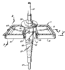
FIGURE 1 is a perspective view of an improved op-
tical flow sensor embodying the novel features of the in-
vention and shown in operatiYe relation with a drip chamber
assembly of an intravenous fluid infusion system;
FIG. 2 is a somewhat schematic horizontal section
view taken generally along the line 2-2 of FIG. 1, showing
emitter and detector blocks with a drip chamber assembly
therebetween;
FIG. 3 is a somewhat schematic vertical section view
taken generally along the line 3-3 of FIG. l;
FIG. 4 is a section view similar to the view shown in
FIG. 2, except that an aperture assembly has been added
within the detector block;
FIG. 5 is an enlarged exploded perspective view of a
lens block;
FIG. 6 i5 a horizontal section view taken generally
along the line 6-6 of FIGo 5; and
FIG. 7 is a vertical section view taken genera~ly
along the line 7-7 of FIG, 5.
DESCRIPTION OF THE PREFERRED EI~BODIMENT
Existing optical flow sensors are characterized by
relatively high manufacturing cost, sensitivity to ambient
-8-
~ 3
optical energy, dirt, and moisture, and the inability to
respond to drops falling far from the vertical axis of a
drip chamber assembly. The present invention employs
unique lens block assemblies to overcome these limitations
and in particular to provide a flow sensor that is respon-
sive to drops falling near ~he walls of ~he drip chamber
as well as to those falling near its vertical axis~
An improved fluid flow sensor embodying the inven~
tion, with a drip chamber assembly in position, is shown
in FIG. 1. The sensor comprises a supporting base 11
having a first arm 13 and a second arm 15 with a space 17
between the two arms. An emitter block 19 having a lens
21 is mounted on arm 13, with lens 21 oriented towards
space 17, and an energy detector block 23 having a lens 25
is mounted on arm 15, with lens 25 oriented to face lens
21 across space 17. A drip chamber a~sembly 27 is posi-
tioned within space 17 between emitter ~ens 21 and detec-
tor lens 25.
Energy emitting chip 29 is installed within cavity
31 in block 19, as shown in FIG. 2 and FIG. 3 ~supporting
base 11 has been omitted from FIG. 2 and FIG. 3 for clari-
ty). Chip 29 is mounted on printed circuit board 33 with-
in block 19 and is located generally at the focal point
of lens 21. A beam of optical energy having rays 35, 37,
39, 41, 43 and 45 is emitted from chip 29 and refracted
_g_
~ 3
by lens 21, and this beam then passes through drip chamber
assembly 27 to lens 25. Lens 25 focuses the beam onto de-
tector chip 47. Detector chip 47 is mounted on circuit
board 49 within cavity 51 of block 23. Detector chip 47
is located generally at the focal point of lens 25.
Drip chamber assembly 27 is generally cylindrical
in shape, as shown in FIGs. 1 and 3. Assembly 27 has trans-
parent cylindrical wall 53 defining drip chamber 5S. An
inlet tube 57 leads into the top of chamber S5. Drop
former 59 comprises an end of tube 57, and as fluid flows
through tube 57, individual drops 61 of fluid form at drop
former 59 and fall through chamber 55 as indicated by
arrow 63 into a reservoir of fluid 65 in the lower portion
of chamber 55. Fluid flows from reservoir 65 out of
cham~er 55 through outlet tube 67. As individual drops 61
of fluid fall through chamber 55, they intersect some of
optical energy rays 35, 37, 39, 41t 43 and 45, causing a
fluctuation in the intensity of the energy beam that
strikes detector chip 47.
Detector chip 47 generates an electrical output
signal that changes in response to fluctuations in the in-
tensity of the optical energy striking the chip. As each
drop 61 of fluid falls through drip chamber 5; and causes
the intensity of the optical energy to fluctuate, the
--10--
.: . . . . -
. ... ..
output signal from chip 47 changes accordingly. Each
change in the output signal is therefore indicative of the
passage of one drop of fluid through chamber 55. Optical
energy from emitter 29 passes through virtually the entire
width of chamber 55, and therefore drops that pass near
the edges of chamb~r ~5, as well as drops that pass through
the center of chamber 55, are detected.
The output signal is applied to electronic monitor-
ing apparatus (not shown). Said apparatus may be configured
to determine the rate of flow of the fluid by measuring
the time interval between the fall of successive drops, or
it may be configured to activate an alert signal if no
drops fall during a predetermined interval of time.
Suitable retaining means ~not shown~ may be
provided to retain drip chamber assembly ~7 in fixed
position in space 17.
The ~ensitivity of the flow sensor can be improved
by increasing the ratio between the width of drops 61 o
fluid and the width of the energy beam that strikes detec-
tor chip 47. This is because the magniSude of a change inthe output signal from chip 47 caused by a ~rop of fluid
intersecting the optical energy beam i5 proportional to the
magnitude of the fluctuation in the intensity of the
energy Deam striking chip 47, and as the percentage of the
total energy beam that is intersected by a drop of fluid
11-
~ ' . .
. ~ ~
.
~ 5~
increases, the magnitude of the fluctuation in beam inten-
sity caused by a falling drop also increases. Since the
size of the drops is governed by other considerations and
cannot be changed for purposes of improving the sensitivi~
ty of the flow sensor~ the only way to increase the ratio
between the drop width and the beam width is to reduce the
beam width. The width of the beam can be reduced by
installing an aperture assembly in detector block 23, as
illustrated in FIG. 4.
The embodiment of the invention shown in ~IG. 4 is
similar to ~hat shown in FIG. 2. For CQnVenienCe, compo-
nents in FIG. 4 that are similar to components in FIG. 2
are assigned the same reference numerals; analogous but
changed components are assigned the same reference nume-
rals accompanied by the letter ~An; and different compo-
nents are assigned different reference numerals.
Aperture assembly 69, having opaque side walls 71,
opaque front walls 73, and an opaque top and bottom (not
shown), is positioned within the hollow area 51 in detector
block 23 with front walls 73 adjacent the ~nterior surface
of lens 25. The top, the bottom, and side walls 71 of as-
sembly 6~ shield detector chip 47 from optical energy that
might enter block 23 through any of its surfaces other than
the surface having lens 25 formed therein. Front walls 73
-12-
::
; .: .. - .. ...... , ., ~ . :
. ~: ~ , : : ' .
extend from side walls 71 part way across lens 25 defining
an aperture 74. Aperture 74 admits optical energy, repre-
sented by rays 39 and 41, that does not pass through extreme
left and right side areas 78 of drip chamber 55, but ex-
cludes optical energy, rPpresented by rays 35A, 37A, 43A,
and 45A, that passes through side areas 78 of chamber 55.
Only energy admitted through aperture 74 strikes detector
chip 47; front walls 73 block o~her energy and scatter it
away.
The width of the energy beam that strike~ detector
chip 47 can be narrowed by making aperture 74 narrower and
widened by making aperture 74 wider~ As the beam o~ energy
that is admitted by aperture 74 becomes narrower, the ratio
of the width of a drop to the total beam width becomes
greater annd chip 47 therefore becomes more sensitive to
drops falling through chamber 55. However, drops that fall
through side areas 78 of chamber 55 are not detected because
the portion of the beam of energy that such drops intersect,
represented by rays 35A, 37A, 43A and 45A, never reaches
chip 47 but instead is scattered away by walls 73. There-
fore, as aperture 74 becomes narrower, side areas 78, within
which falling drops cannot be detected, become wider. The
tradeoff, then, is that as aperture 74 becomes narrower,
chip 47 b~cornes more sensitive to falling drops but the
portion of drip chamber 55 within which falling drops can
be detected becomes narrower,
-13-
`:~
- :.
::
If drip chamber assembly 27 is constrained in a
perfectly vertical position, drops 61 will fall only through
the center of drip chamber 55 and will be detected even if
a very narrow aperture 74 is used. But as assembly 27 is
tilted farther away from a vertical orientation; drops 61
will tend to fall closer and closer to the edges of
chamber 55, and if assembly 27 is tilted ~ar enough, the
drops will fall through one of the ~ide areas 78 and
detector chip 47 will fail to respond to themO
In other words, as aperture 74 becomes narrower,
chip 47 becomes more sensitive and the maximum til~ angle
of drip chamber 55 at which drops can be reliably sensed
becomes smaller. ~ useful compromise is to make aperture
74 narrow enough that each of side areas 78 is as wide as
one drop. This compromise gives good sensitivity and
enables the sensor reliably to detect the passase of drops
through a drip chamber assembly that is tilted not more
than 26 degrees from the vertical.
Optionally, opaq~e baffles 75 can be installed with-
in aperture assembly 69 between front walls 73 and detector
chip 47. Baffles 75 form a surface parallel to front walls
73 and defining a second aperture 76 that is narrower than
aperture 74. Baffles 75 reduce the effects on chip 47 of
am~ient optical energy by scattering much of ~uch energy
away. Still further immunity to such ambient energy can be
-14-
.. . .
`'' ''''' ~
.,. , .~.. - , ,.,.. ~ . ,
, ~
~ 3
achieved by adding a second set of baffles 77, and even more
such baffles could also be added, as will be apparent to
those skilled in the art.
Turning now to a more detailed description of energy
emitter block 19, said block is formed from a hollow block
of transparent material as shown in FIG. 5. Rear side 79
of block 19 has an opening 81 into cavity 31 in the inter-
ior of block 19. Lens 21 ;s formed in front side 83 of
block 19, said lens having a convex exterior surface 85
and a convex interior surface 87. The shapes of exterior
and interior surfaces 85 and 87 of lens 21 are formed
according to the refractive effects of the walls of drip
chamber assembly 27; in the preferred embodiment described
and illustrated herein, exterior lens surface 85 is convex
both in its horizontal cross-section and in its vertical
cross-section as shown in FIGs. 6 and 7, respectively, and
interior lens surface 87 is convex only in its horizontal
cross~section.
Energy emitting chip 29 is installed on circuit
board 33 and is connected to printed wiring conductors 89.
Wires 91 are connected to conductors 89 for making connec-
tions between chip 29 and an external circuit (not shown)O
A shoulder 93 is formed along the perimeter of open-
ing 81,~said shoulder being recessed a short distance into
cavity 31, said distance being slightly greater than the
-15-
, .. , .. . : .
.~ .
-
,
...
3s~
thickness of circuit board 33. Circuit board 33 has the
same width and length as does opening 81, and the circuit
board is positioned in said opening against shoulder 93.
Notches 95 in circuit board 33 engage alignment keys 97
extending rearwardly from shoulder 93, retainin~ circuit
board 33 in fixed orientation with respect tc block l9.
Lens 21 is formed such that chip 27 is generally at the
focal point of lens 21 when circuit board 33 is positioned
against shoulder 93 with notches 9S engaging alignment
keys 97.
When circuit board 33 is in position against shoulder
93 within opening 81, the circuit board closes off the only
access between cavity 31 and the outside worl~, and the cir-
cuit board in combination with the interior edges 99 of
opening 81 defines a recessed area lOl. Recessed area 101
may be filled with potting material (not shown), thereby
sealing block l9 and protecting cavity 31 from dust, mois-
ture, or other contaminants that may be present in the at-
mosphere. Ideally, assembly and potting of circuit board
33 into block 19 will be performed in a dry, inert atmos-
phere such as nitr~gen~ The assembled block can then be
washed or subjected to dusty or other harsh atmospheres
without harming chip 29 or causing condensation on interior
lens surface 87.
-16
. .~ . :.
, ~
:. - . ,
53
The structure of detector block 23 is generally
similar to the structure of emitter block 19, except that
the chip 47 installed within the former is an optical ener-
gy detecting device whereas the chip 29 installed within
the latter is an optical energy emitter. Also, the t~o
lenses have slightly different focal lengths. In addition,
in the preferred embodiment described and illustrated here-
in, interior surface 88 of detector lens 25 is convex both
in its hori~ontal cross-section and in its vertical cross-
section, as shown in FIG. 3, whereas interior lens surace
87 of emitter lens 21 is convex only its hori~ontal cross-
section. It will be understood, therefore, that the preced-
ing description of the structure of emitter block 1~ also
pertains to the structure of detector block 23 except as
noted in this paragraph.
A fluid flow sensor as described can be used with any
drip chamber assembly having transparent walls and being of
a physical size that will fit within the space 17 between
emitter block 19 and detector block 23.
I~munity to ambient optical energy is good because
lens 25 tends not to focus such light onto detector chip
47. This immunity can be improved by using an aperture
assembly 69, and if desired may be still further improved
by empl~y;~ an energy emitter that emits infrared energy
and a filter or other mean~ (not illustrated) to render
-17-
: '
- :.- ,:: -
:: , ,.. : :: :
detector chip 47 insensitive to any op~ical energy that is
not within the infrared spectrum.
Assembly of a fluid flow sensor embodying the present
invention is simpler than assembly of a prior art sensor.
Instead of having to align physically small energy emit-
ters and energy detectors with respect to a sensor base
and with respect to each other, an assembler need only
mount ~he two lens blocks so that their lenses face one
another. In addition, a fluid flow sensor embodying the
present invention needs no additional shielding from am-
bient energy and, because the energy detector and emitter
chips are sealed, the only op~ical parts that must be kept
free of dust and moisture are the exterior lens surfaces
of the two blocks. The present invention also provides a
sensor responsive to drops falling far from the vertical
axis of the drip chamber, and therefore works equally well
with drip chamber assemblies that are tilted as much as 26
degrees as with vertically-oriented assemblies.
of course, many variations and modifications of the
present invention are possible in light of the above teach-
ings. For example, the radii of curvature of the various
lens surfaces may be changed to correct for the different
refractive effects of various different drip chamber assem-
blies. Moreover, although the inventivn has been disclos2d
in the specific context of an IV fluid flow monitor, it has
-18-
_.
.
.,. ', ~
.. . .
:
~ ~ ~ 8 ~
application to any product in which it is desirable to meas-
ure fluid flow or sense the lack of such flow by optical
means. It ;s therefore to be understood that, within the
scope of the appendeci claims, the invention may be practiced
otherwise than as specifically described.
19-
.
: ~