Note: Descriptions are shown in the official language in which they were submitted.
~;~6~
--1--
Description
Power Supply Adap~ y~
Technical Field
.
This invention relates to power or voltage supply
systems and, more particularly, to a power or voltage supply
system which provides an output voltage of a given magnitude
from a first supply source having a voltage of the given
magnitude and alternatively from a second supply source
having a voltage of a magnitude significantly different from
that of ~ igiven magnitude.
Background Art
Reduced scaling or shrinking of the geometries of
devices used in integrated semiconductor circuit technology
for forming denser circuits has required voltage supply
sources to provide lower voltages than the heretofore
generally accepted standard supply voltage of 5 volts,
particularly in order to avoid a voltage breakdown in the
insulation layers. During the transition from 5 volt
supplies to the lower voltage oupplies of, say, J.3 volts, a
mix of circuits is being used wherein some of the circuits
have been designed for use with standard 5 vo]t supplies
while other circuits have been designed for use with the
lower 3.3 volt supplies. In general, the geometries of
memory circuits are reduced at a faster rate than are the
geometries of logic circuits which are coupled to the memory
circuits. Accordingly, a voltage mismatch results during
this transition period when multiple levels of power
supplies coexist in a given system.
~U9-86-016
i8~ L9
--2--
In U. S~ Patent 4,469,959, filed b~ K. Luke et al on
Mareh 15, 1982, there is diselosed a eireuit for controlling
the supply voltage to a eomplementary metal oxide
semieonduetor (CMOS) inverter eireuit which uses first and
S seeond voltage souree~ wherein a voltage magnitude variation
in the first supply souree eauses the seeond supply source
to be eonneeted to the inverter circuit.
U. S. Patent 3,076,135, filed by ~. P. Farnsworth et al
on September 29, 1958, diseloses a transistor power supply
system which turns off under an overload condition and turns
on upon the removal of the overload.
U. S. Patent 4,3~9,627, filed by J. Tabata on March 27,
1979, discloses a detecting circuit for a power source
voltage whieh ineludes a reference voltage generating
eireuit, a voltage dividing eireuit and a voltage comparing
eireuit.
U. S. Patent 4,463,270, filed by J. S. Gordon on July
24, 1980, diseloses a eomparator eircuit for deteeting a
differenee in relative magnitudes of two voltages which is
suitable for controlling a battery backup power supply.
Disclosure of the Invention
It is an object of this invention to provide a simple,
low leakage power supply adapter system having an output
voltage of a given magnitude regardless of whether the
magnitude of the input voltage is at the given magnitude or
higher than the given magnitude.
BU9-86-016
~2613~
--3--
. ~ .
In accordance with the teachings of this invention, a
power supply adapter system is provided which includes a
voltage supply source terminal, an output terminal,
switching means coupled to the voltage supply source and
including first and second switches, the first switch being
disposed between the voltage supply source terminal and the
output terminal, voltage conversion means serially connected
with the second switch and disposed between the voltage
supply source terminal and a point of reference potential,
such as ground, and having an output coupled to the output
terminal, and means for detecting first and second ranges of
voltages at the power supply source terminal and for
producing first and second control voltages, respectively,
the first control voltage being applied to the first switch
and the second control voltage being applied to the second
switch.
The foregoing and other ob~ects, features and
advantages of the invention will be apparent from the
following more particular description of the preferred
embodiments of the invention, as illustrated in the
accompanying drawings.
Brief Description of the Drawings
Fig. 1 illustrates primarily in block Eorm the power
supply adapter system of the present invention, and
Fig. 2 is a circuit diagram of a preferred embodiment
of the system of the present invention.
Best Mode for CarrYinq Out the Invention
Referring to ~ne drawings in more detail there is
illustrated primarily in block form in Fig. 1 the power
supply adapter system of the present invention which
includes a power ~upply source terminal 10 and a detector
BU9-86-016
12, which may be any standard voltage detector, connected
between the power supplv source terminal 10 and a point of
reference potential, such as ground. The power supply
adapter system also includes a voltage converter 14 having
an output connected to an output terminal 16. The voltage
converter 14 is designed to produce a constant output
voltage VDD, when activated~ having a magnitude lower than
the voltage at the power supply source terminal 10. A
switching circuit 18 includes a first switch 20 connected
between the power supply voltage source terminal lO and the
voltage converter 14 and a second switch 22 disposed between
the power supply source terminal 10 and the output terminal
16. The detector 12 is designed to produce a first control
voltage indicative of a first range of voltages at the power
supply source terminal 10 and a second control voltage
indicative of a second range of voltages at the power supply
source terminal 10. The first control voltage from the
detector 12 is applied to a conductive line ENABLE R
connected between a first output of the detector 12 and the
first switch 20 of the switching circuit 18 and the second
control voltage from the detector 12 is applied to a
conductive line ENABLE P connected between a second output
of the detector 12 and the second switch 22 of the switching
circuit 18.
In the operation of the system of the present invention
illustrated in Fig. 1 of the drawings, when the magnitude of
the voltage at the power supply source terminal 10 exceeds a
given voltage, e.g., 4.2 volts, as may be provided from a
nominal 5 volt power supply source, the detector 12 produces
the first control voltage on ENABLE R line which closes the
first switch 20 of the switching circuit 18. With the first
switch 20 closed, the voltage converter 14 is activa-ted to
produce at the output terminal 16 the voltage VDD having a
desired magnitude of, e~g., 3.3 volts. If the voltage at
the power supply source terminal 10 is lower than the given
voltage, the detector 12 produces the second control voltage
BU9-86-016
on ENA~LE P line which closes the second switch 22 of the
switching circuit 18, with the first control voltage opening
the first switch 20. With the second switch 22 closed, the
low voltage, i.e.,the 3.3 volts, at the power supply source
terminal 10 is directly applied to the output terminal 16,
while the voltage converter 14 is rendered inoperative by
the opening of the first switch 20. Thus, a relatively low
and constant output voltage VDD of, say, 3.3 volts, is made
available at the output terminal 16 regardless of whether a
+5 volt power supply VH or a +3.3 volt power supply VH is
- connected to the power supply source terminal 10.
Accordingly, the adapter circuit of the present invention
permits a 3.3 volt supply technology to be powered by either
a 5 volt or a 3.3 volt supply.
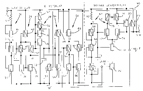
In Fig. 2 of the drawings, there is shown a circuit
diagram of a preferred embodiment of the system of,the
present invention. The circuit of Fiy. 2 is made in the
CMOS technology with P-channel field effect transistors
being indicated by a rectangle with a diagonal line formed
therein and a gate electrode and with ~-channel field effect
transistors being indicated by a rectangle without a
diaaonal line and a gate electrode. Furthermore, elements
in the circuit of Fig. 2 which are similar to the elements
of the system of Fig. 1 are identified by the same
characters. The circuit of the present invention
illustrated in Fig. 2 includes the detector 12 having a
first comparator circuit or differential ampliEier 24, a
first bias network 26 for providing a substantially constant
reference voltage and a control voltage cir,cuit 28 for
providing a voltage which linearly varies with the voltage
at the power supply source terminal 10. The first bias
network 26 includes N-channel field effect transistors 30,
32 and 34 serially arranged with a first resistor ~1,
preferably having a resistance of more than one megaohm and
formed in an N-well in CMOS technology, connected between
the power supply source terminal 10 and a point of reference
BU9-86-016
--6--
potential~ such as ground. Each of the transistors 30, 32
and 34 are arranged as diodes. The first comparative
circuit 24 is disposed between the power supply source
texminal 10 and a point of reference potential and includes
S bleeder devices 36 and 38~ preferably made as N-channel field
effect transistors, and control devices 40 and 42 and a load
device 44, preferably made as P-channel field effect
transistors. The control voltage circuit 28 includes an
output terminal or node C having a plurality of ~-channel
field effect transistors, such as transistors 46 and 48
connected between node C and a point of reference potential
and a plurality of P-channel field effect transistors, such
as transistors 50 and 52jconnecte~ betweerL the node C and
the power supply source terminal 10. The control gates of
each of the transistors 46~ 48, 50 and 52 are connected to
node C. It should be understood that many more serially
arranged N-channel and P-channel transistors can be used in
the control voltage circuit 28, if desired. A first
low-pass filter capacitor Cl is connected between the output
or node A of the bias network 26 and a point of reference
potential and a second low-pass filter capacitor C2 is
connected between node C of the control voltage circuit 28
and a point of reference potential. The detector 12 further
somprises a buffer or invexter circuit 54 which includes
N-channel field effect transistor 56 and P-channel field
effect transistor 58. The input to the buffer circuit 54
is connected to the output terminal or node B of the first
comparative circuit 24. Node D of the buffer circuit 54
is connected to an Enable P line which is also connected to
the control gate of the second switch 22, preferably a
P-channel field effect transistor, connected between the
power supply source terminal 10 and the output terminal 16.
An interface circuit 60 designed to match the characteris-
tics of the second switch 20, which is preferably an
N-channel field effect transistor, includes serially ar-
ranged transistors 62, 64 and 66, with
transistors 62 and 66 being of the N-channel type and
BU9-86-016
~6~ 9
--7--
~ .
transistor 64 being of the P~channel type. Transistors 62
and 64 form an inverter and transistor 66 is arranged as a
diode. An output terminal or node E provided between
transistors 62 and 64 is con~ec~ed to the Enable R line which
is also connected to the gate electrode of the first switch
20, preferably an N-channel field effect transistor.
.
The voltage converter 14 includes a second comparator
circuit 68 having N-channel field effect transistors 70, 72
and 74 and P-channel field effect transistors 76 and 78.
The output terminal or node F of the second comparator
circuit 68 is connected to a control gate of a pass device
80, preferably an N-channel field effect transistor, con-
nected between the power supply source terminal 10 and the
output terminal 16. Transistor 70 acts as a current source,
transistors 72 and 74 act as control devices and transistors
76 and 78 act as current limiters for the second comparative
circuit 68. The voltage converter 14 further includes a
second bias network 82 for pro~iding a constant reference
voltage having an output terminal or node G. The bias
network 82 includes serially arranged P-channel field effect
transistors 84, 86 and 88 disposed between node G and a
point of reference potential and a second resistor R2,
preferably having a resistance of more than one megaohm and
~ormed in an N-well in CMOS technology, disposed between
node G and the power supply source terminal 10. Node G is
connected to the control gate of the transistor 70 and to
the control gate of the transistor 72. The output terminal
16 is connected to the control gate of transistor 74. A
third low-pass ~ilter capacitor C3 is connected between node
G of the second bias network 82 and a point of reference
potential.
A conductive feedbac}c line 90 is connected. from the
output terminal 16 to the control gate of a P-channel
bleeder transistor 92 and to the control gate of a P-channel
bleeder transistor 94. Transistor 92 is serially connected
~U9-86-016
--8--
. .
with an N-channel bleeder transistor 96 between node I of
the interface circuit 60 and ground and transistor 9~ is
connected between node C of the control voltage circuit 28
and ground. The control gate of the transistor 96 is
connected to node E of the interface circuit 60.
..
In the operation of the power supply adapter system of
the present invention illustrated in Fig. 2 of the drawings,
node ~ of the first bias network 26 of the detector 12
provides a substantially constant reference voltage, between
1.3 and 2.0 volts, with voltages at the power supply source
terminal 10 as low as about 2 volts. This constant
reference voltage is applied to the control gate of the
control device 40 of the first comparator circuit or
differential amplifier 24. The voltage at node C o~ the
control voltage circuit 28 varies linearly with the voltage
at the power supply source terminal 10. The detector 12 is
designed so that when the voltage at terminal 10 is at 4.2
volts or higher, the voltage at B of the first comparator is
low, which produces a high voltage at node D of the buffer
circuit 54. This high voltage is sufficient to maintain the
switch or the P-channel pass transistor 22 off. Thus, the
voltage at the power supply source terminal lO is not
applied directly to the output terminal 16.
With node B at a low voltage, the P-channel transistor
6~ of the interface circuit 60 is turned on while the
N-channel transistor 62 is off. Thus, node E is at a high
voltage, which is sufficient to turn on the first switch or
N-channel transistor 20 to activate the voltage converter
14. The voltage converter 14, which operates under normal~
feedback principles, is designed so that a voltage at node F
of the second comparator circuit 68 applied to the control
gate of the N-channel transistor 80 maintains the output
voltage VDD at the output terminal 16 at 3.3 volts as long
as the voltage at the power supplv source terminal 10 is
above 4.2 volts. As the voltage VDD on the output terminal
BU9-86-016
_9_
16 varies so does the current through transistors 7~ and 78
The voltage at node H, which is proportional to the current
flowing through transistors 70 and 72 assists in controll.ing
the voltage magnitude at the output terminal 16. The
current path through transistors 74 and 78, the curxent path
through transistors 72 and 76 and the voltage at node H
together regulate the voltage at node F in direct response
to the voltage on output terminal 16. The voltage at node F
biases the control gate of the pass transistor 80 which
supplies current to the output terminal 16.
When the voltage at the power supply source terminal
10 is below, say, 3.8 volts, such as when a 3.3 voltage
source is connected to the power supply source terminal, the
voltage at node B of the first comparator circuit or
differential amplifier 24 of the detector 12 goes high
turning on N-channel transistor 56 of the buffer circuit 54
to discharge the output node D of the buffer circuit 5~.
The voltage at node D is decreased to a point where the
second switch-or P-channel transistor 22 turns on hard so as
to directly connect the power supply source terminal 10 to
the output terminal 16. Meanwhile, since node ~ of the
first comparator circuit 24 of the detector 12 is at a high
voltage, N-channel transistor 62 of the interface circuit 60
turns on to discharge node E thereof. Discharging node E
lowers the voltage at the control gate of the first switch
or N-channel transistor 20 to turn off transistor 20 and,
thus, render the voltage converter inoperative. The power
supply adapter system of the present invention as
illustrated in Fig. 2 of the drawings can provide
substantia.lly constant output voltages at output terminal 16
to magnitudes as low as 2.0 volts. .
It should be noted that the detector 12 has two main
functions, tl) to monitor the power supply voltage VH at
terminal 10 and (2) to turn off and on the voltage converter
14. Furthermore, it can be seen that the circuit of Fig. 2
BU9-86-016
--10--
has a hysteresis of 400 millivolt, between VH = ~.2 volts
and VH = 3.~ volts, built in to provide essential and
desirable noise immunity characteristics.
Accordingly, it can be seen that a simple power supply
adapter circuit has been provided which supplies an output
volta~e of, say, 3.3 volts regardless of whether a 5.0 volt
source or a 3.3 volt source i~ connected to the power supply
source terminal 10.
It should also be noted that by using CMOS technology
to make the system of Fig. 2 of the drawings, the current
leakage between the power supply source terminal lQ and
ground is very low, even though some of the current paths
between the terminal 10 and ground, such as the first bias
network 26, do not use complementary devices. The paths
which do not use complementary devices have minimal
current leakage since they use very small devices and high
resistivity resistors. Accordingly, the circuit of Fig. 2
of the drawings can be readily used in battery backup
applications with a data retention mode in, e.g., six device
static random access memory at voltages on terminal 10 down
to 2 volts.
While the invention has been particularly shown and
described with reference to preEerred embodiments thereof,
it will be understood by those skilled in the art that
various changes in form and details may be made therein
without departing from the spiri.t and scope or the
invention.
BU9-86-016