Note: Descriptions are shown in the official language in which they were submitted.
~æ~
.,.~
E~E~
This invention relate to the field of
electrical manufacturing, and particularly to means for
tinning the conductors of components suppli~d on taped
rolls, in situ on the tapes.
It is advantageous for commercial users of
electrical components to be able to purchase much used
components in large quantities, for later use as
needed. To facilitate these large p~rchases, suppliers
sometlmes package components by mounting them between
long tapes wound on spools or reels,,which are easily
.
~;~ stored by the purchasers, and from which the components
are easily accessible.
In industr~al applications, components:are
advantageously positioned physi~ally on circui:t boards
~ : with their conductors extending~through holc8 in
:~ conductive patterns on the boards, to which patterns
they are connected by wave solderlng. This means that
the solderabllity~of the component conductors must~be
good~at the;time of use~ regardless of how long~a period
of s~orage~has occurred~
25 ;~
r
'~.
:
~. ~
: ' , , ~' ~; .
Various suppliers use various finishes on the
component conductors, however: coa~ings of gold,
silver, and tin are known, which may be of different
thicknesses, porosities, and surface contamination. It
5 has been ound that a considerable amount of "touch upi'
action is often required after wave soldering, to
perfect connections which were not made satisfactorily,
and this is an expensive, manual process. The period of
storage between purchase and use also has an
10 unpredictable affect on the solderability of the
component's conductors.
One way of overcom.ing this is to hand-tin all
the conductors as the components are taken from the
storage reels and before they are mounted on the circuit
boards, but this iæ also a very costly and time
~: consuming process.
RIEE ~MMA~Y OF TH~ I~V~NTIQ~
i~
The present invention comprises apparatus for:
: automatically tinning the leads of tape-stored
electrical components, immediately upon receipt from the
suppliers, without removing the components from the
; tapes. This has been found to overcome the tendency of
the leads to become unsolderable with time, and can be
: done rapidly, automatically, and ine*pensively
irrespective~of the sur~ace treatment of ~he conductors
. :
~ as supplied. ~he arrangemen~ is equally e~fective for
,
` ; ~
/
~ ,
:. ~
~2~
- 3 - 64159-866
components with "axial leads" extending to tapes in opposite
directions from opposite ends of the components, and for com-
ponents with "radial leads", extending to a single tape in a
single direction from the component. Practice of the invention
results in a supply of components of consistent solderability
at any time of use no matter how they were originally supplied.
In accordance with the present invention, there
is provided in combination: a wave station establishing a wave
of liquid solder having a convex configuration trans~erse of an
axis, which decreases in cross-sectional area with distance in
a first direction along said axis; means transporting along
said axis in said direction an electrical component haviny at
least one linear conductor extending transverse to said axis to
pass through said wave, and further means located heyond said
wave for removing from said conductor any excessive solder
remaining thereon, including heating means to maintain said
excess solder in liquid phase, and suction means for drawing
said excess solder from said conductor.
In accordance with another aspect of the invention,
there is provided in combination: a wave station establishing
a wave of liquid solder having a convex configuration, transverse
to an axis, which decreases in cross-sectional area with
distan¢e in a first direction along said axis; and means trans-
porting along said axls in said direction an electrical compon-
ent having at least one linear conductor extending transverse
to said axis to pass through sald wave.
In accordance with another aspect of the invention,
there is provided in combination: a wave station establishing
a wave of liquid solder having a convex configuration, trans-
verse to an axis, which decreases in cross-sectional~area with
. , .
39~7
- 3a - 6~159-~66
distance in a first direction along said axis; and means tran-
sporting in said direction along said axis a succession of
electrical components, each having conductors extending trans-
verse to said axis, to initially pass through and subsequently
emerge from said wave, said components being oriented so that
said conductors slope downwardly from said components, and means
located beyond said wave for removing from said conductors any
excess solder remaining at the lower ends thereof.
In acco.rdance with another aspect of the invention,
there is provided apparatus for tinning predetermined portions
oE conductors extending transversely in opposite directions
from a succession of electrical components carried on tape means
orthogonally interconnecting the opposite ends of said
conductors, comprising means movi~g said tape means and said
components generally horizontally along a path including, in
succession: a feed reel; a precleaning station having nozzle
means applying cleaning solution to said conductors; a fluxing
. ~ ,
station having foam head means for applying liquid flux to said
~: portions of said conductor; means orienting said tape means
so that first conductors slope downwardly from first ends of
said components; a first solder wave station establishing a wave
; of liquid solder having a convex configuration transverse io
said path so that said chosen portions of said first conductors
.; pass through and emerge from said wave, said wave station
.~ including means for removing excess solder from the lower ends
~- of said first conductor; means reorienting said tape:means so
: that second conductors slope down~ard from second ends of said
components; a second solder ~ave station establishing a wave
of liquid solder having a convex configuration transverse to
- 30 said path so that said chosen portions of said second conductors
,: ~
, ~ , '':, '' ' .; ~
.
. . .
-3b - 6~159-866
pass through and emerge from said wave, said second solder wave
station including means Eor removing excess solder from the
lower ends of said second conductors; a cooling station; a post
cleaning station having nozzle means applying rinsing liquid to
said portions of said conductors; a drying station; and a take
up reel.
In accordance with another aspect of the invention t
there is provided apparatus for tinning predetermined portions
of conductors extending transversely from a succession of
electrical components carried on tape means orthogonally inter-
connecting the ends of said conductors, comprising means moving
said tape means and said components generally horizontally along
a path including, in succession: a feed reel, a precleaning
station having nozzle means applying cleaning solution to said
predetermined portions of said conductor; a fluxing station
having foam head means for applying liquid flux to said portions
of said conductors; means orienting said tape means so that flrst
conductors slope downwardly ~rom first ends of said components,
a solder wave station establishing a wave of liquid solder
ha~ing a convex configuration transverse -to said path so that
said chosen portions of said conductors pass through an emerge
from said wa~e, sald wave station including means for removing
:"
;~ excess solder from the lower ends of said conductors; a cooling
station; a post cleaning station having nozzle means applying
rinsing liquid to said portions of said conductors; a drylng
; station; and a take up reel.
~arious advantages and features of novelty which
characterize the invention are pointed out with particularity
in the claims annexed hereto and forming a part thereoE. ~ow-
ever, for a better understanding of the invention, its
~'
' ' '"
39~
.
- 3c - 6415~-866
advantages, and objects attained by its use~ reference should
be had to the drawing which for.ms a further part hereof, and
to the accompanying descriptive matter, in which there is
illustrated and described a preferred embodiment of the inven-
tion.
BRIEF DESCRIPTION OF THE DRAWING
In the drawing, in which like reference numerals
identify corresponding parts throughout the several views,
FIGURE 1 shows a portion of a supply of components as packaged
with axial leads, FIGURE 2 is a block diagram of a lead wire
tinning system according to the invention, FIGURE 3 is a plan
view of a portion of the invention, FIGURE 4 is a fragmentary
pl.an ~iew of a portion of FIGURE 3 to a larger scale, FIGURE
5 is a fragmentary sectional view along the line 5-5 of FIGURE
;.
~'~
;~ ~
,.. :
.: :
.~,
,
.;.:
,
:: .
: . ,. ".. . ,
:,: , .,,.. . . ~ . : . .
_4_ ~2~ 3~
4 showing a component in place, FIGURE 6 is a
fragmentary section view along the line 6-6 of FIGURE 4
showing a component in place, FIGURE 7 is a view like
FIGURE 5 but taken along the line 7-7 of FIGUR~ 3, and
FIGURE 8 shows a portion of a supply of components as
packaged with radial leads.
E~ D ~ESCRIPTI~ O~ THE P~EFER~D-E~Q~l~E~
Referring now to FIGURE 1, there is shown a
portion of a supply of electrical components as packaged
for tape storage. Here a plurality of diodes 11 have
axial leads 12 and 13 extending from opposite ends
thereof in opposite directions. A first adhesive
support tape 14 extends orthogonally to the free ends o
leads 12 and a second support tape 15 extends
orthogonally to the free ends of leads 13, so that the
assembly comprises what may be called a~ribbon" 16 of
~ ~ components. It is desired to retin or solder-coat the
-~ ~ portions "ar of each lead, as these are the portions
which will later be used in assembllng circuitry~ ~
2Q Liquid solder should not be applied to portions "b" as
the resulting heat may be de~rimental to the components,
and similarly portions "c" should not be contacted with
solder to avold heat degredation of tapes 14 and 15~
; FIGURE 2 shows that in the apparatus ribbon 16
25 ~ is drawn from a fe~d reel 20 to a drlven take-up reel 21
along a path havlng a number of treatment stations.
.
~i : :
::
~ '~ '
I
!
_5 ~:26~39~
Except as will presently be pointed out, the conductors
of the components remain generally horizontal while
following this path. This may be conv~niently arranged
by providing properly spaced and oriented rails in which
tapes 14 and 15 are guided, the tapes being extended
beyond the components at each end of the ribbon to lead
the latter into and out of the equipment.
The path is identified by the general reference
numeral 30, and includes in sequence a precleaning
station 31, a fluxing station 32, a first twi ting
station 33, a irst solder wave station 34, a reverse
twisting station 35, a second solder wave station 36, a
cooling and untwisting station 37, a post cleaning
station 38, and a drying station 39.
Precleaning station 31 has nozzle means for
:~ applyin~ cleaning solution to the condoctorsO Fluxing
station 32 has foam head means ~or applying liquid flux
.
to the conductors, particularly to portions "a'~
thereof. In twisting station 33 the tape is twisted to
an angle of approximately~20 degrees so:that leads l~
slope downwardly from componentc 11. This orientation
~: is main~ained through first solder wave s~a~ion 34,
wh~ich will b~ described~elow. In second twisting
station 35 the twist~is:r;everced so~that leads 13 slope
;25~ ~ downwards from compon~nts~}I. After:passing solder wave
station 36 the~ribbon pacses through coolin~ station 37
.,~.: :
,:
'~ ' .
~;268~9~
--6~
which, if desired, includes fan or blowing means, and in
which the ribbon is restored to a normal horizontal
orien~ation. Postcleaning station 38 has nozzle means
directing a stream of water to flow against the soldered
conductors, and the components and tapes are dried by
suitable means in station 39 for discha ge to take-up
reel 21, after which they may be stored until the
components are needed for use. Except for stations 34
and 36, the stations are generally known structures.
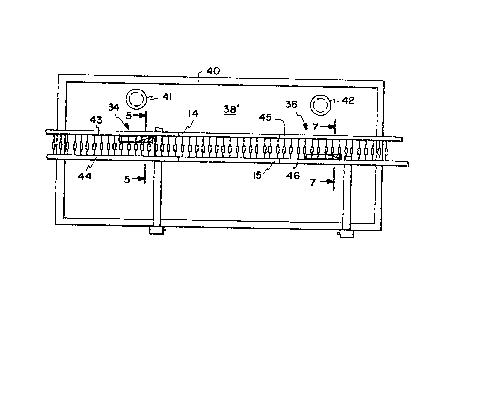
Turning now to FIGURE 3, a satisfactory
embodim~n of stations 33 to 37 is shown to comprise a
chamber or tray 40, with heat-insulating walls, in which
a supply of solder 38' is malntained molten by suitable
heating means not shown. Liquid solder is con~inuously
~:~ lS pumped from chamber 40 by a first li~uid metal pump 41
to first solder wave station 34, and similarly liquid
: solder i8 continuously supplied from ~ray 40 by a second
liquid metal pump 42 to second solder wave station 36.
Ribbon 16 is drawn from left to right past station 34 in
- tracks 43 and 44, which terminate just beyond station
34r Then the ribbon ~s drawn past station 36 in tracks
: 45 and 46~, which begin jus~ before station 3~. Tracks
43 and 44 cause ribbon 16 ~o twist from a nominal
horizontal orlentation by about 20 degrees in a first
: 25~ direction, track 44~and tape 15 being higher than track
43~ and tape l4. On the other hand,~track 45 is higher
~ ~
- ~L26~9~
- 7 - 64159-~66
than track 46, 50 that in these tracks tape 14 is higher than
tape 15 and the ribbon is twisted to an orientation displaced
from the horizontal by about 20 degrees in the opposite
direction. The gap between tracks 43, 44 and tracks 45, 46
comprises reverse twisting station 35. Tape 14 travels first in
~rack 43 and then in track 45, while tape l5 travels first in
track 44 and then in track 46, so that a forty degree twist in
ribbon 16 occurs. By this arrangement portions "a" of leads 12
are retinned at station 34, and then portions "a" of leads 13
are retinned at station 36, as will now be described.
Stations 34 and 36 are similar, and only one will be
described in detail. Station 34 includes a vertical riser or
chimney 50 in which upward flow of molten solder is maintained
by a suitable pump: pumps of this sort are commercially
available. At the top of a chimney one side 51 is lower than
the other side 52, ana has a rolled edge as indicated at 53 over
. ,
which the solder 38' flows. The ribbon 16 of components moves
across the top of chimney 50 from end 5S to end 56, as indicated
by the arrow 57.
~0 A wave shaper 60 is provided in chimney 50 to change
the~shape of the solder wave emerging from the chi~ney: the
wave shape near end 55 is indicated at 61 in FIGURE 5, and the
:: :
~ wave shape near end 56 is indicated
., ., ~
, .1, ' .
-.;
:''''~
'
' ~
97
~ 8-
at 62~ Tapes 14 and 15 move past chimney 50 in rails 43
and 44 so positione~ that when each component first
enters the solder wave most of its length, portion "a"
is submerged, but as the ribbon proceeds the submerged
length of conductor 12 decreases. By this arrangement
any excess solder on conductor 12 runs toward the lower
. end to form what may loosely be termed an nicicle" 65,
although lt is in liquid rather than solid ætate.
If allowed to solidify, such icicles would
seriously interfere with the subsequent incorporation of
the components in the circuit boards, and so forth, 50
means is provided or removing the excess solder before
it solidifies. Immediately adjacent to end 56 of
chimney S0 there is provided a heated block 70 having a
port 71 positioned for near passage by the components as
they leave the chimney. A vacuum line 72 connects port
71 with a collection jar~73 which ls maintained at
subatmospheric pressure by a suitable pump connection
; 74. As each conductor 12 passes port 71, any "icicle"
of excess liquid solder is pneumatically removed to ~ar
. 73.
For most satis~actory flow of liqu~d solder, it~
ha~; been found helpful to modi~fy edge 51 by providing a
slight surve 75, and to provide block 70 with a recess
25 76, to enable slight: flow of liquid metal in the
: direction of movement o~ the ribbon.
~''`
I
t
~ r ~
9 ~ 7
Station 36 is like station 34 except that the
top of the chimney is bevelled in the opposite
direction, and the rails lead conductors 13 through the
solder instead of conductors 12~ It will be apparent
: 5 that if components are being treated which have radial
rather than axial leads, only one tape and one solder
: wave station are necessary.
Numerous characteristics and advantages of the
invention have been set forth in the foregoing
description, together with details of the strucl:ure and
function of the invention, and the novel features
thereof are pointed out in the appended claims. The
disclosure, however, is illu~trative only, and changes
may be made in detail, especially in matters of shape,
:: : 15 size, and arrangement of parts, within the principle of
the invention, to the full~extent indicated by the ~road
~ general meaning of the terms in which the appended
:~ : claims are expressed.
2~
' ~ : `
:
.
~ 25 ~ :
. ~ :, : :
:: ,,.
~ ~'
,,' .
'
,