Note: Descriptions are shown in the official language in which they were submitted.
~2~
The present invention relates to an automatic
gain control (AGC) circuit for controlling gain of a
video signal in a television receiver, the AGC circuit
being applicable to an AGC operation of a video signal
in which the offset processing is randomly applied to,
for example, the sync signal for scrambling the video
signal in pay television.
AS is generally known, an AGC circuit maintains
gain at a constant level. In a television receiver, for
example, the AGC circuit detects the signal level of the
video signal obtained by video detection. Based on the
detected level, the AGC circuit controls the gain of an
intermediate amplifier circuit (IF circuit) and that of
a radio frequency circuit (RF circuit) in the tuner.
The AGC operation for the IF circuit is called IFAGC,
while that for the ~F circuit is called RFAGC~
These two types of AGC operation, RFAGC and IFAGC,
are required in order to obtain a compromise between the
noise figure and the cross-modulation distortion. In
order to obtain a good noise figure, the greater the
gain of the RF circuit, the better. However, a high-
gain RF circuit tends to generate a distorted signal due
to the nonlinearity involved in an amplifier in the RF
circuit. This distorted signal causes cross-modulation
intererence. Thus, the RF circuit and the IF circuit
must be subjected to the AGC control, in order to obtain
satisfactory performance with respect to both the noise
-- 2 --
figure and the cross-modulation interference.
In general, in the amplifier, by a distinguished
nonlinearity, the following relation holds between the
input signal voltage and the output signal voltage of
the amplifier.
m
Y (e) = ~ Knen .-. (1)
n=l
where Y (e) i5 the output signal voltage of the ampli-
fier
e is the input signal voltage of the amplifier
Kn is the coeEficient expressing the linearity
of the amplifier
n is the distortion factor
In the above relation (1), the nonlinearity distor-
tion contains the distortion components of very high
order. However, the distortion components, which must
be considered in practical use, are those which are, at
most, up to the secondary order (n=2) or the tertiary
order (n=3).
When the distortion as given by expression (1)
above is produced in a tuner, cross-modulation inter-
ference and beat interference occur. The degree of
cross-modulation, which represents the degree of cross-
modulation interference, is proportional to the square
of the signal giving rise to the cross-modulation inter-
ference. The cross-modulation interference appears
noticeably in a system having a number of transmission
~2g~ 3
channels, such as a CATVo
Beat interference occurs when a number of high-
Erequency signals are concurrently transmitted, and
also occurs if the distorted component generated in the
amplifler is present within the frequency band of the
high-frequency signal.
When RFAGC is performed on the RF circuit having a
plurality of mixers, an RF amplifier is provided at the
prestage of the first mixer. The gain of the RF ampli-
fier is controlled in order to reduce distortion. Thisapproach is satisfactory from a viewpoint of reducing
the distortion, but is not good from a viewpoint of
reducing the C/N (carrier-to-noise) ratio. The C/N
ratio is generally yiven as
C/N [dB] = ei [dB~] - NF [dB] - 0.86dB .......... (2)
where ei is the input signal vol-tage of the amplifier,
and NF is the noise figure. Let the number of cascade-
connected amplifiers to be "m", and then the overall C/N
ratio (C/N)m is given as
(C/N)m [dB] - (C/N) [dB] - 10 loglo m ........... (3)
The overall C/N ratio (C/N)m is inversely proportional
to the number "m" of cascade-connected amplifiers. This
means that when number "m" of amplifiers with the same
performance are connected in a cascade fashion, the C/N
ratio is degraded by 10 loglo m [dB].
Therefore, in order that the C/N ratio, when the
amplifiers of "m" stages are cascade-connected, is kept
~Z~3~3
-- 4
at that for a single stage of amplifier, the input
signal level ei at each ampliEier is given as
ei [dB~] = e min [dB~] + 10 loglo m ... (4)
where e min is the minimum signal level as calculated by
using expression (2) above.
As can be seen from the above relation, in order to
obtain a predetermined C/N ratio, it is required that
the signal be at a predetermined level. Therefore, the
gain oE an RF amplifier having a function for improving
the C/N ratio must be kept at such a value as not to
impair the distortion characteristics.
When "m" stages of amplifiers are connected in a
! cascade Eashion, the overall noise figure NFt is given
as
NF2 - 1 NF3 - 1 NFm-l
NFt = NFl + Gl GlG2 + GlG2..-Gm-l
... (5)
where Gl, G2,... Gm are the power gains of respective
amplifiers, and NFl, NF2,... NFm are the noise figures
of the respective amplifiers.
Expression (5) shows that the greater gain of the
RF amplifier provides a satisfactorily low noise figure.
For the above reasons, the AGC operation is per-
formed on the RF circuit and the IF circuit. The RF
circuit is controlled so as to suppress the distortion,
and the IF circuit is controlled so that the signal gain
is kept constant.
:~L2~ 3
-- 5 --
In recent years, pay-television, such as CATV has
been developed. Various types of protection systems
have been incorporated in such pay-television system, in
order to prevent people other than the subscribers from
watching the television. In one of the protection
systems, a scrambled signal, for example, is used as
a broadcast signal. By using a descramble circuit, pro-
vided in the subscriber's terminal, the scrambled signal
is descrambled, and a normal video signal is obtained.
Various systems are used for scrambling the video
signal. These include RF scramble and base band scram-
ble. The base band scramble can be classified into the
video insertion system, the sync offset system, and the
sync suppress system.
Pay-television such as CATV receives a multi-
channel broadcast signal. In this case, due to the
nonlinearity distortion of the active elements in the RF
amplifier and in the mixer for frequency-converting in
the tuner, an unwanted distorted signal, as expressed
by expression (1) above, is generated. The distorted
signal, or cross-modulation distortion, affects the
video signal. In order to prevent the effect by this
distortion, the gain of the tuner is controlled.
The input field strength (AGC delay point) at which
the RFAGC operation is initiated in consideration of
cross modulation distortion level and the noise figure
is determined. In other words, the field strength at
~Z~ 3
which ~FAGC operation is initiated together with IFAGC operation,
is determined. Thus, the gain of the input signal is suitably
controlled.
AS a result, optimal gain control of the input signal
is performed by the IFAGC and RFAGC operations. However, the AGC
operations have to follow up the change of the input level.
This requirement causes problems, especially when the
AGC operation is performed in relation to a video scrambled
u signal whose horizontal sync siynal is made offs~t. That is to
say, ~ull consideration has to be taken for the response
: characteristics of the IFAGC and RFAGC.
Accordingly, the present invention provides an AGC
1~ circuit in which the response characteristic of the RFAGC can be
controlled without impairing the response characteristic of the
IF~GC, and in which, therefore, a stable AGC can be performed on
the arrival wave signal such as the scrambled signal lacking the
sync signal.
2~
In accordance with the present invention invention, an
automatic gain control (AGC) circuit is provided for controlling
the gain of a video signal in a television receiver, which
comprises: a tuner which has an input terminal for receiving a
2~ video signal at a radio frequency (RF), an RF amplifier for
amplifying the RF video signal which is received at the input
terminal, a frequency-converter
3~ .
3~
~ 6 -
~2G~3
-- 7 --
for frequency-converting the RF video signal, amplified
by the RF amplifier, into an intermediate-frequency (IF)
video signal, and an output terminal for outputting the
IF video signal coming from the frequency-converter; an
IF amplifier for receiving the IF video signal output
from the output terminal of the tuner, and for amplify-
ing the received IF video signal; a detecting circuit
for receiving the output signal of the IF amplifier, and
for video-detecting the received output signal; an IFAGC
circuit for receiving the detected output signal of the
detectiny circuit, and for generating a voltage signal
for controlling the gain of the IF amplifier, in accor-
dance with the level of the detected signal received; a
first time-constant circuit, for receiving the voltage
signal generated by the IFAGC circuit, for applying a
first time-constant to the received voltage signal, and
for supplying the received voltage signal with the first
time-constant, as an IFAGC voltage signal, to the IF
amplifier; an RFAGC circuit for receiving the IFAGC
voltage signal, and for generating a voltage signal
for controlling the gain of the RF amplifier of the
tuner, in accordance with the level of the received
IFAGC voltage signal; a second time-constant circuit,
for receiving the output voltage signal of the RFAGC
circuit, for applying either a second or third
time-constant to the received output voltage signal,
and for supplying the received output voltage signal
:~L2~ 3
with -the second or third time-constant, as an RFAGC voltage sig-
nal, to the RF amplifier of the tuner, the second and third time-
constants being longer than the first time-constant; and a time-
constant controller for receiving the output voltage signal of
the RE~AGC circuit, and for controlling the time-constant of the
second time-constant circuit, in accordance with the change in
level of the received output voltage signal.
In one embodiment of the present invention said time-
constant control means includes means ~or controlling the time-
constant of said second time-constant circuit means, so that when
the change in level of the output voltage of said RFAGC circuit
means is greater than a predetermined value, said third time-con-
stant is selected, and said third time-constant is shorter than
said second time-constant. Suitably said control means includes
means for operating to decr~ase a resistance of said second time-
constant circuit means when the change in level of the output
voltage of said RFAGC circuit is greater than a predetermined
value. Desirably said second time-constant circuit means com-
prises a series circuit including first and second resistors anda first capacitor, which are connected in series to the output
terminal o~ said RFAGC circuit means, and a second capacitor,
connected in parallel to the series circuit, and said ~FAGC
voltage signal is derived from the node between said second
resistor and said first capacitor; and said operating means inc-
lude bypass means for causing the signal to by-pass the second
resistor of said second time-constant circuit means when the
change in level of the output voltage of said RFAGC circuit means
is greater than a predetermined value. Preferably said bypass
0 means includes non-linear element means which is connected in
parallel to the second resistor of said second time-constant
circuit means. Suitably said non-linear element means includes a
first non-linear element connected in parallel to the second
resistor of said second time-constant clrcuit means, which is
conductive when an increase in the output voltage signal of said
RFAGC circuit means exceeds a predetermined value; and a second
::~2~ 3
non-linear element connected in parallel to the second reslstor
of said second time-constant circuit means, which is conductive
when a decrease in the output voltage signal of said RFAGC cir-
cuit Ineans exceeds a predetermined value. Desirably said first
non-linear element is a diode, the anode of said diode being con-
nected to the node between the first resistor and the secondresistor of said second time-constant circuit means, and the
cathode of said diode being connected to the node between the
second resistor and the first capacitor of said second time-con-
stant clrcuit means; and said second non-linear element is a
lo diode, the anode of said dlode being connected to the node
between the second resistor and the first capacitor of said s~c-
ond time-constant circuit means, and the cathode of said diode
being connected to the node between the ~irst resistor and the
second resistor of said second time-constant circuit means
Preferably the circuit further comprises means for causing said
first time-constant to be temporarily longer than said second and
third time-constants during a turning transition.
In another aspect thereof the present lnvention pro-
vides an automatic gain control (AGC) circuit for controlling a
gain of a scrambled video signal in which the sycn signal is ran-
domly offset from a video signal for a cable television receiver
comprising tuner means having input terminal means for receiving
a scrambled video signal at a radio ~requency (RF), RF amplifier
means for amplifying the RF scrambled video signal which is
received at said input terminal means, fre~uency-converting means
fo~ frequency-converting the RF scrambled video signal amplified
by said RF amplifier means, into an intermediate-frequency (IF)
scrambled video signal, and output terminal means for outputting
the IF scrambled video signal coming from said frequency-convert-
ing means; IF amplifier means for receiving said IF video scram-
bled signal output from the output terminal means of said tuner
means, and for ampli~ying the received IF scrambled video signal;
detecting circuit means for receiving the output signal of said
IF amplifier means, and for video-detecting the received output
- 8a -
signal; IFAGC circuit means for recelving output signal of said
detecting circuit means, and for generating a voltage for con-
trolling the gain of said IF amplifier means, in accordance with
the level of the detected signal received; first time-constant
circuit'means, for receiving the voltage signal generated by said
I~AGC circuit means, for applying a first time-constant to the
recelved voltage signal with said first time-constant, as an
IFAGC voltage signal, to said IF amplifier means; RFAGC circuit
means for receiving said IF~GC voltage signal, and for generating
a voltage signal for controlling the gain of said RF amplifier
lo means of said tuner means, in accordance with the level of said
received IFAGC voltage signal; second time-constant circuit
means, for receiving the output voltage signal of said RFAGC
circuit means, for applying either a second or third time-consant
to the received output voltage signal, and for supplying the
received output voltage signal with the second or third time-
constant, as an RFAGC voltage signal, to said RF amplifier meansof said tuner means, said second and third time-constants being
longer than said first time-constant; and time-constant control
means for receiving the output voltage signal of said RFAGC
circuit means, and for controlling the time-constant the detected
time-constant circuit means, in accordance with the chanye in
level of the received output voltage signal.
In a still further aspect of the present invention an
automatic gain control (AGC) circuit for controlling a gain of a
scrambled video signal in which the sync signal is randomly off-
set from a video signal for a cable television receiver compris-
ing tuner means having input terminal means for receiving a
scrambled video signal at a radio frequency (RF), RF amplifier
means for amplifying the RF scrambled video signal which is
received at said input terminal means, fre~uency-converting means
for freguency-converting the RF scrambled video signal amplified
by said RF amplifier means, into an intermediate-frequency (IF)
scrambled video signal, and output terminal means for outputting
the IF scrambled video signal coming from sa~d frequency convert-
- 8b -
:~L2~ 3
ing means; IF amplifier means for receiving said IF video scram
bled signal output from the output terminal means of said tuner
means, and for amplifying the received IF scrambled video signal;
detected circult means for receiving the output signal of said IF
amplifier means, and for video-detecting the received output
signal; descramble circuit means for receiving the detected
output signal from said detecting circuit means, and for desc-
rambling said scrambled video signal; IFAGC circuit means for
receiving the output signal of said descramble circuit means, and
~or generating a voltage signal for controlling the gain of said
lo IF amplifier means, in accordance with the level of said output
signal of said descramble circuit means; flrst time-constant
circuit means for receiving the voltage signal generated by said
IFAGC circuit means, for applying a first time-constant to the
received voltage signal, and for supplying the received voltage
signal with said first time-constant, as an IFAGC voltage signal,
to said IF amplifier meas; RFAGC circuit means for receiving said
IFAGC voltage signal, and for generating a voltage signal for
controlllng the gain of said RF ampllfier means of said tuner
means, in accordance with the level of said received IFAGC
voltage signal; second time-constant circuit means for receiving
the output voltage signal of said RFAGC circuit means, for apply-
ing either a second or third time-constant to the received output
voltage signal, and for supplying the received output voltage
signal with the second or third time-constant, as an RFAGC
voltage signal, to said RF amplifier means of said tuner means,
sald second and third-time-constants being longer than said first
time-constant; and time-constant control means for receiving the
output voltage signal of said RFAGC circuit means, and for con-
trolling the time-constant of said second time-constant circuit
means, in accordance with the change in level of the received
output voltage signal.
This invention can be more fully understood from the
following detailed description when taken in conjunction with the
accompanying drawings, in which:-
- 8c -
lZ~ 3
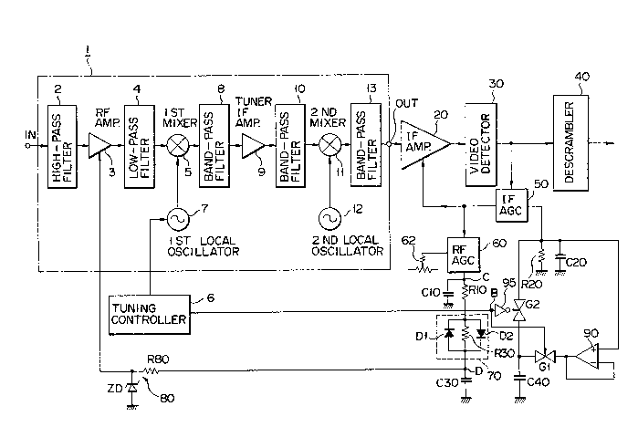
Fig. 1 is a circuit diagram of an embodiment of an AGC
circuit according to this invention;
Fig.s 2A to 2D show waveform charts for explaining a
prior AGC operation, in which Fig. 2A shows the waveforms of the
video detection output, Fig. 2B IFAGC voltage waveform, Fig. 2C
reproduced video waveform, and ~ig. 2D horizontal sync output
waveform;
Fig.s 3A to 3D show waveform charts, respectively cor-
responding to Fig.s 2A to 2D, for explaining the opera-tion of the
AGC circuit of Fig. l;
Fig.s 4A to 4D show waveforms of the signal during a
tuning transition for channel selection at circuit points in the
Fig. 1 AGC circuit; and
Fig. 5 shows a waveform of the RFAGC voltage during the
tuning transition in the AGC circuit of Fig. 1.
An embodiment according to the present invention
- 8d -
43
g
will now be described, with reference to the accompany-
ing drawings.
Fig. l shows an ~GC circuit of this invention,
which is used in connection with a video signal cir-
cuit for processing a scrambled video signal in pay-
television such as CATV. Various signal-scramble
systems are used. In the description to follow, a sync
offset system, for randomly offsetting the sync signal,
is taken as an example.
In the figure, a scrambled mu]ti-channel CATV sig-
nal is input to (up and down) tuner 1. In tuner 1, the
input signal is supplied to RF amplifier 3 via high-pass
filter 2. RF amplifier 3 is a gain-variable amplifier.
The gain of the amplifier is adjusted mainly for setting
the nonlinearity distortion, given by the expression
(1), to an appropriate value. The output of RF ampli-
fier 3 is supplied to Eirst mixer 5 via low-pass filter
4. First local oscillator 7 outputs an oscillating
Erequency corresponding to the broadcast station spe-
cified by tuning controller 6. By using the output offirst local oscillator 7, first mixer 5 high-frequency
converts the television signal from RF amplifier 3. The
high-frequency converted output of first mixer 5 is
amplified by tuner IF amplifier 9 af-ter its unwanted
signal is removed by band-pass filter 8. Then, it is
supplied to second mixer 11 via band-pass filter 10. By
using the output of second local oscillator 12, second
-- 10 --
mixer 11 low-frequency converts the high-frequency con-
verted television signal. The low-frequency converted
signal is output to output terminal OUT of tuner 1 via
band-pass -filter 13.
The output of tuner 1 is input to IF amplifier 20.
Through the IFAGC operation, the gain of IF amplifier
20 is controlled so that the noise figure given by the
expression (5) is not impaired, and its output is kept
at a predetermined constant level. The output of IF
amplifier 20 is supplied to video detector 30, where
video detection is performed. The detected video sig-
nal is supplied to descrambler 40, where the descrambl-
ing processing is executed to reproduce the video
signal.
The output of video detector 30 is also supplied
to IFAGC circuit 50. IFAGC circuit 50 generates an
IFAGC DC voltage which corresponds to the level of the
video-detected output. The gain of IF amplifier 20 is
controlled by the generated IFAGC voltage. The time-
constant for the IFAGC is set by resistor R20 and capa-
citor C20.
The output of IFAGC circuit 50 is also supplied to
RFAGC circuit 60. RFAGC circuit 60 executes the called
AGC delay to make the RFAGC follow the IFAGC operation,
and generates an RFAGC voltage for controlling the gain
of RF amplifier 3 of tuner 1. The volume of the AGC
delay is set by variable resistor 62.
~~
-- 11 --
The output of RFAGC circuit 60 is supplied to a
parallel circuit made up of capacitor C10, and a series
circuit including resistor R10, time-constant controller
70 and capacitor C30. Controller 70 is made up of two
diodes, Dl and D2, and resistor R30, which are connected
in parallel. Capacitor C10 is for removing the video
component.
The RFAGC voltage is derived Erom the connection
point D of time-constant controller 70 and capacitor
C30. The RFAGC voltage is supplied to the RF amplifier
3 of tuner l, via clamp circuit 80. Clamp circuit 80
is for clamping the RFAGC voltage to below a AGC control
level of RFAGC amplifier 3. Clamp circuit 80 comprises
resistor R80 and zener diode ZD.
Time-constant controller 70 has a configuration
such that, in accordance with the change in value of the
output voltage of RFAGC circuit 60, it selects the RFAGC
time-constant. As is described above, time-constant
controller 70 comprises diodes Dl and D2, and resistor
R30 which are connected in parallel. When the output
voltage change of RFAGC circuit 60 exceeds diode volt-
age, either of the diodes is made conductive. When
diode Dl or D2 is conductive, a time-constant of the
time-constant circuit, which is connected to the output
of RFAGC circuit 60, is approximately (C10 + C30) x Rl0.
On the other hand, when the output voltage change
of RFAGC circuit 60 is less than the forward voltage of
- 12 -
the diode, diodes Dl and D2 are in an off state. In
this case, the time-constant is approximately (Cl0 +
C30) x (Rl0 + R30). Since resistor R30 is a high-
resistance type, this time-constant is longer than that
when diode Dl or D2 is conductive.
~ ote here that diodes Dl and D2 are not made con-
ductive simultaneously. If an increase occurs in the
output voltage of RFAGC circuit ~0, which exceeds the
diode voltage, diode D2 is conductive. Conversely, if a
decrease occurs in the output voltage, which exceeds the
diode voltage, diode Dl is conductive. In this way,
time-constant con-troller 70 controls the time-constant
in the RFAGC, in accordance with the change in value of
the output voltage of RFAGC circuit 60.
As recalled, in the AGC operation, the gains of IF
amplifier 20 and oE RF amplifier 3 of tuner l are con-
trolled, allowing for the signal noise figure and the
cross-modulation distortion. In this case, the response-
time characteristic must also be taken into considera-
tion. Generally, the response time of the RFAGC must be
shorter than that of the IFAGC. One reason for this is
that the IFAGC is performed on the signal which is ob-
tained after the video detection, and is a demodulated
video signal itself. Another reason is that the RFAGC
executes the AGC operation with retardation with respect
to the IFAGC operation, and prevents characteristics
degradation, such as the cross-modulation distortion.
- 13 -
The AGC detection in the AGC operatlon is classi-
fied into a peak AGC detection, an average AGC detec-
tion, and a keyed AGC detection. In this embodiment,
the peak detection is employed, for example.
Assuming that the video signal input to the Fig. 1
circuit is a scrambled video signal in which the sync
signal is randomly made offset, as is shown in Fig. 2A.
The IFAGC voltage decreases because the sync signal at a
low level is detected at time tl. At time t2 when a sig-
nal whose sync signal is made offset, the IFAGC voltage
increases, as is shown in Fig. 2B. Thus, even if there
is no extreme variation in the level of the image signal
of the video signal, the gain of the IF amplifier 20 is
unintentionally increased because the sync signal is made
offset. This resu]ts in the generation of flickers in
the reproduced image. In an extreme case, the image sig-
nal of the reproduced video signal is amplified to below
the normal pedesta] level, or even below the reference
level VREF for the sync separation, as is shown in
Fig. 2C. In this case, the normal sync separation be-
comes difficult, as is shown in Fig. 2D, and the de-
scrambling operation becomes impossible to perform.
To avoid this, the capacitance of capacitor C20
constituting the time-constant circuit of the IFAGC, is
increased, to reform the waveform oE the IFAGC voltage,
as is shown by a one-dot-chain line in Fig. 2B. This is
done irrespective of the arrival of the sync offset
- 14 -
voltage signal. In other words, by increasing the capa-
citance of capacitor C20 which is connected to the out-
put terminal of IFAGC circuit 50, the IFAGC is effective
-for the video signal lacking the horizontal sync signal.
However, when the IFAGC time-constant is long,
the time-constant for the RYAGC must also be set long,
because the RFAGC must operated with some delay from the
IFAGC operation. Therefore, the RFAGC time-constant
must also be increased. The mere increase of the RFAGC
time constant results in the degradation of the response
characteristics of the RFAGC. To avoid this, in this
invention, if sudden change occurs in the output voltage
of RFAGC circuit 60, which exceeds the diode voltage,
either diode D1 or D2 is made conductive, in order to
lS compensate for the degradation of the response char-
acteristics oE the RFAGC.
As is described above, with the increase the IFAGC
time-constant, the AGC delay is performed while the
RFAGC time-constant is controlled by time-constant
controller 70. As a result, a stable AGC operation is
ensured. Therefore, even if no horizontal sync signal
is contained in successive several lines, as is shown in
Fig. 3A, a stable IFAGC voltage can be obtained as shown
in Fig. 3B, as compared with the IFAGC voltage shown in
Fig. 2B. Consequently, the reproduced video signal is
not amplified until it goes below the reference level
VREF, either, as is shown in Fig. 3C, and the normal
- 15 -
sync separation is possible, as is shown in Fig. 3D.
Stabilization of the AGC system is required not
only when the above scrambled video signal arrives, but
also during the tuning transition. A circuit for stabi-
lizing the system during the tuning transition is con-
nected to IFAGC circuit 50. As is shown, a parallel
circuit of resistor R20 and capacitor C20 for setting
the time-constant of IFAGC circuit 50, is connected in
parallel with capacitor C40. Capacitor C40 is connected
so as to be charged and discharged via buffer amplifier
90 and gate Gl, and discharged via gate G2. Gates Gl
and G2 are gated by a select signal supplied from tuning
controller 6. Gate G2 is supplied with the select sig-
nal via inverter 95, so that when gate Gl is on, gate G2
will be oEf.
Therefore, during the tuning transition, gate Gl is
conductive, and the output of IFAGC voltage circuit 50
is connected to capacitor 40. First, capacitor C40 is
charged by the IFAGC voltage. The operation during the
tuning transition will now be described, with reference
to the timing charts of Figs 4A to 4D. As is shown in
Fig. 4A, from time tl of tuning till time t2 when the
select signal at point B of Fig. 1 changes its state
(Fig. 4B), capacitor C40 is actively charged to a prede-
termined value. At -time t2, gate Gl is turned off.
This quickens the stabilization of the IFAGC voltage
during tuning transition. In response to this,
:~2~ 3
- 16 -
a sudden change in the voltage at point C, i.e., the
output voltage of RFAGC circuit 60, is prevented. From
time t2 onl gate G2 is conductive, to quicken the stabi-
lization of the IFAGC voltage. Therefore, as is shown
by a solid line in Fig. 4D, the voltage at point D,
i.e., -the RFAGC voltage, settles down more quickly than
in the prior art, in which it does not settle down till
time t3, as is shown by a dotted line in Fig. 4D.
Fig. S shows a variation of the RFAGC voltage
during the tuning transition. In the figure, the solid
line represents the transition characteristics when
capacitor C40 is not charged during the tuning transi-
tion and when time-constant controller 70 is not oper-
ated. A bro)cen line describes how the RFAGC voltage is
stabilized or settles down during the tuning transient.
This stabilization results from the cooperation oE the
transient charge to capacitor C40 with the operation of
time-constant controller 70.
As can be seen Erom the graph, even if the IFAGC
time-constant is increased to a certain degree so as
to cope with the the scrambled signal, which is formed
by subjecting the input video signal to the offset
processing, and with the case that the electric field
strength is suddenly changed due to fluttering, for
example, the RFAGC voltage can be stabilized, and
therefore, the stabilization of the AGC system is
realized, thus stabilizing the AGC control system.
- 17 -
Thus, irrespective of the state of the arrival signal,
both the RFAGC and IFAGC can be optimumly controlled,
satisfying the requirements for the signal distortion
and noise figure performance.
As has been described above, in the AGC circuit
according to this invention, with provision of time-
constant controller 70 in the RFAGC circuit, the re-
sponse characteristics of the RFAGC can be controlled
without impairing the response characteristics of the
IFAGC operation. Therefore, even if the input signal
is a scrambled signal lacking the horizontal sync
signal, a stable AGC operation can be secured. It
should be noted here that the RFAGC voltage controls
the AGC time-constant only when the change in level of
the RFAGC voltage exceeds a predetermined level. This
feature enables the RFAGC to appropriately control the
time-constant so that the AGC system will be stabilized,
while keeping its follow-up characteristic for a varia-
tion in the level of the arrival signal.
The AGC circuit according to this invention is
applicable for control of the RFAGC time-constant, not
only when the peak AGC detection is used, but also when
other types of AGC detection, such as the keyed AGC de-
tection, are used.
Even when any type of AGC detecting means is used,
the response characteristic and the gain control of the
RFAGC can be optimumly controlled, thus not impairing
~2~ 3
- 18 -
the noise figure and the signal distortion character-
istic~
While the present invention has been described, by
way of example, in connection with a CATV using a
scrambled video signal, it should be understood that
this invention is applicable for the normal TV set for
receiving the normal broadcasting TV programs.
As recalled, in the above-mentioned embodiment,
the output signal of video detector 30 is received.
Such a modification of the embodiment, whereby the video
signal descrambled by descramble circuit 40 is received,
is within the scope of this invention.