Note: Descriptions are shown in the official language in which they were submitted.
~9463
JITTE:R MEASUREMENT METHOD AND APPARATUS
_CKGROUND OF THE INVENTION
The present invention relates to a method and apparatus
for measuring the timing jitter of a tributary data stream
that has been multiplexed into a higher-rate multiplex
stream u~ing pulse stuffing techniques.
Timing jitter is the short term variation of the sig-
nificant instants of a data -signal from their expected or
average positions, the amplitude and frequency of this
variation constituting the amplitude and frequency of the
jitter waveform. Various ways of measuring the timing
1~ jitter of a data signal are known, one such way being
described in US patent no. 3,737,765 (Lubarsky). In this
patent, the jitter amplitude of a signal is determined by
comparing the actual zero crossings of the signal with their
expected occurrences as predicted by an averaging process
15 carried out on the previous actual occurrences of the zero
crossings.
The present invention is concerned with the measurement
of the timing jitter of a data signal where the signal has
been multiplexed into a higher-rate multiplex stream using
20 pulse stuffing techniques. Pulse stuffing is a process
where the bit rate of a digital tributary stream is brought
up to the rate of occurrence of time slots for that tribu-
tary in the multiplex stream by the insertion of a dummy bit
or the repetition of selected tributary bits, each insertion
25 or repetition constituting a ~stuff". Each stuff may be
viewed as advancing the phase of ~he tributary stream
relative to a reference representing the average rate of
occurrence of tributary time slots in the multiplex stream,
the phase of the tributary thereafter falling back relative
30 to the reference until the next stuff causes a further
advance. The rate of tributary phase slippage between
stuffs is, of course, dependent on the discrepancy between
the tributary frequency and that of the aforesaid reference.
In practice, stuffin~ opportunities are only presented
~;
1~9463
at fixed intervals corresponding to predetermined time slots
in the multiplex stream; whether or not any particular
stuffing opportunity is taken up will depend on the current
phase lag of the tributary relative to the reference. Of
course, in order to enable stuffed bits to be removed when
demultplexing the tributary from the multiplex stream, it is
necessary to provide some indication in the multiplex stream
as to whether a time slot that could have been stuffed, does
in fact contain a stuffed bit. This indication takes the
form of stu~fing control bits inserted at known locations in
the multiplex stream.
Where the tributary data signal is free of jitter, it
will lose phase at a constant rate dependent on the
tributary frequency and this phase loss will be compensated
for by stuffs at regular intervals. However, where the
tributary exhibits jitter, its phase loss will not be at a
constant rate with the result that stuffing will occur
irregularly.
S~MMARY_OF THE INVENTION
.
The present invention provides apparatus for measuring the
timing jitter of a tributary data stream that has been
multiplexed into a high-rate multiplex stream using pulse
stuffing techniques, the multiplex stream including stuffing
control bits indicative of the presence or absence of stuffs
at predetermined positions in said multiplex stream. The
apparatus includes monitoring means for receiving and
monitoring the multiplex stream to detect the stuffing
control bits included therein that relate to said trihutary,
the monitoring means being arranged to output both a first
signal indicative of the occurrence of a stuff relating to
said tributary, and a second signal indicative of the
multiplex stream timing. The apparatus further includes
first processing means arranged to receive said first and
second signals and to derive therefrom an average~rate
~i9'~3
signal indicative of the average rate of phase loss of the
tributary as compared to a notional reference related to the
multiplex stream timing, and second processing means for
deriving a jitter signal representative of the timing jitter
of the tributary. The second processing means is arranged
to receive both the said first signal and said average-rate
signal and is operative to derive therefrom a current value
for said jitter signal by updating a preceding value of the
jitter signal, this updating involving increasing the jitter
signal value by a predetermined amount for each stuff
indicated by said first signal while effecting a decrease in
jitter signal value at an average rate dependent on the
value of said average-rate signal.
Where the tributary is jitter free, the increases in
jitter value resulting from the presence of detected stuffs
are equalled by the cumulative decrease reflecting the said
average rate of phase loss. Where tributary jitter is
present, however, the sum of the stuff related increases
will differ from the cumulative decrease, the difference
being indicative of the change in jitter value over the
peciod under consideration.
The said average rate of phase loss could, for example,
be determined by the first processing means in terms of the
average time between stuffs; preferably, however, the
stuffing ratio of the tributary is used as a measure of said
average rate of phase loss (the stuffing ratio being a ratio
relating the actual number of stuffs effected to the number
of stuffing opportunities). More particularly, in jitter
measurement apparatus as set out in the last preceding
paragraph but one, the first processing means is preferably
arranged to determine the stuffing ratio of the tributary
with the second signal being used in this determination to
provide an indication of the occurrence of each stuffing
opportunity relating to the said tributary, and the first
processing means being further arranged to output as said
4 ~j9'~63
average-rate signal a signal indicative of said stuffing
ratio. The second signal can be derived directly from
the stuffing control bits though this is not essential
inasmuch as equivalent timing information could be
derived, for example, from framing bits included in the
multiplex stream.
In one preEerred embodiment, the first and second
processing means are jointly implemented as a digital
filter arranged to receive said first signal as its
input signal and to be clocked by said second signal at
a rate corresponding to the rate of occurrence of
stuffing opportunities relatin~ to said tributary, the
transfer function of the digital filter being such that
the output of the filter is representative of the timing
jitter of said tributary.
Various aspects of the invention are as follows:
Apparatus for measuring the timing jitter of a
tributary data stream that has been multiplexed into a
higher-rate multiplex stream using pulse stuffing
techniques, the multiplex stream including stuffing
control bits indicative of the presence or absence of
stuffs at predetermined position in said multiplex
stream, sa.id apparatus comprising:
monitoring means for receiving and monitoring said
multiplex stream to detect the said stuffing control
bits included therein that relates to said tributary,
the monitoring means producing both a first signal
indicative of the occurrence of a stuff relating to said
tributary, and a second signal indicative of the
multiplex stream timing;
first processing means responsive to said first and
second signals to derive therefrom an average-rate
signal indicative of the average rate of phase loss of
the tributary as compared to a notional reference
related to the multiplex stream timing; and
second processing means for deriving a jitter
signal representative of the timing jitter of said
tributary, the second processing means responsive to
i ~
~;..
4a 3L~ ~946;3
both the said first signal and said average-rate signal
to derive therefrom a current value for said jitter
signal by updating a preceding value of the jitter
signal,this updating involving increasing the jitter
signal value by a predetermined amount for each stuff
indicated by said first signal while effecting a
decrease in jitter signal value at an average rate
dependent on the value of said average-rate signal.
Apparatus for measuring the timing jitter of a
tributary data stream that has been multiplexed into a
higher rate multiplex stream using pulse stuffing
techniques, the multiplex stream including stuffing
control bits indicative of the presence or absence of
stuffs at predetermined positions in said multiplex
stream, said apparatus comprising:
monitoring means for receiving and monitoring
the multiplax stream to detect the stufing control bits
included therein that relate to said tributary, the
monitoring means producing both a first signal
indicative of the occurrence of a stuff relating to said
tributary, and a second signal indicative of the
multiplex stream timing, and
a digital filter receiving said first signal
as its input signal and clocked by said second signal at
a rate corresponding to the rate of occurrence of
stuffing opportunities relating to said tributary, the
transfer ~unction of the digital filter being such that
the output of the filter is representative of the
timing jitter of said tributary.
A method of measuring the timing jitter of a
tributary data stream that has been multiplexed into a
higher-rate multiplex stream using pulse stuffing
techniques, the multiplex stream including stuffing
control bits indicative of the presence or absence of
stuffs at predetermined positions in said multiplex
stream, said method comprisin~ the steps of:
monitoring the multiplex stream to detect the
~.~
~,
4b 1 ~ ~94~3
stuf f ing control bits included therein that related to
said tributary;
utilising the stuffing control bits to determine
both the occurrence of a stuff relatiny to said
tributary and the stuffing ratio of the tributary; and
deriving a current value for a jitter signal
representative of the tributary timing jitter by
updating a preceding value of the jitter signal, this
updating involving increasing the jitter signal value
for each stuff detected while effecting a decrease in
value at an average rate dependent on the value of the
stuffing ratio.
. ,
,, ~, . ~
63
BRIEF DESCRIPTION OF THE DRAWINGS
~ . . _
There now follows a detailed description which is to be read
with reference to the accompanying drawings of digital
jitter measurement apparatus; it is to be understood that
the digital jitter measurement apparatus has been selected
for description to illustrate the invention by way of
example and not by way of limitation.
In the accompanying drawings:
Figure 1 is a diagrammatic depiction of the multiplex-
ing of four DSl tributaries into a DS2 multiplex stream;
Figure 2 is a diagram of the M-frame and subframe
structure of a DS2 stream;
Figure 3 shows various time graphs illustrating the
derivation of a tributary jitter signal from the stuffing
information contained in the multiplex stream;
Figure 4 is a block diagram of a basic circuit for
deriving the stuffing ratio of a tributary;
Figure 5 is a block diagram of a basic analog circuit
for deriving a tributary jitter signal according to a
procedure outlined with reference to Figure 3;
Figure 6 is a block diagram of a dual-microprocessor
processing arrangement of the preferred Eorm of jitter
measurement apparatus embodying the invention;
Figure 7 is a block diagram of a dual-microprocessor
processing arrangement of the preferred form of jitter
measurement apparatus;
Figure 8 is a flow chart of the main jitter measurement
routines of the Figure 7 dual-microprocessor arrangement;
and
Figure 9 is a flow chart of a measurement settling
check routine for the Figure 7 arrrangement.
DESCRIPTION OF THE PREFERRED EMBODIMENT
.
The jitter measurement apparatus to be described here-
inafter is intended to monitor a DS2 multiplex stream in
order to determine the timing jitter of a selected one of
~x~
the four DSl tributaries multiplexed into the DS2 stream
(the designations DSl and DS2 refer, of course, to the well
known Bell digital hierarchy widely used in the North
American continent).
As indicated in Figure 1, four DSl tributaries (of a
nominal rate of 1.544 Mb/s) are multiplexed into a common
DS2 stream using pulse stuffing techniques. More partic-
ularly, the DS2 stream is divided into a succession of M-
frames that occur at a rate of 5376 M-frames/sec and each M-
frame includes, for each tributary, 288 time slots arranged
to accommodate corresponding bits of the tributary.
The rate of occurrence of time slots/tributary in the
DS2 frame structure is, in fact, arranged to be slightly
greater than th~ bit rate of the tributaries; thus, for
example, one of the DS1 tributaries may have a bit rate
equivalent to 287.5 bits per M frame and will, therefore,
lose phase relative to the M-frame structure at half a bit/
M-frame. To compensate for this phase loss, an opportunity
is provided once every M-frame for one of the bits of the
DSl tributary to be repeated whereby to bring the effective
bit rate of the DSl tributary up to that of the rate of
occurrence of time slots for that tributary in the DS2
stream. This opportunity to repeat a bit is termed a
stuffing opportunity and the actual repetition of a bit is
known as a stuff; in the example previously given where the
DSl tributary has an actual bit rate equivalent to 287.5
bits/M-frame, every other stuffing opportunity is taken up
in order to bring the effective DSl bit rate up to the rate
of occurrence of M-frame time slots, that is 288 time slots/
M-frame. The possibility of taking up or ignoring a stuf
fing opportunity once every M-frame permits variations of
the DSl bit rate to be compensated for, the maximum stuffing
rate being 5376 stuffs/sec (that is, the M-frame rate).
Figure 2 shows the detailed structure of each M-frame,
each such frame being composed of four subframes, Ml to
M4. Each subframe is, in turn, composed of six groups of
;~
i3
49 time slots, the first one of each of which contains a
control bit while the remaining 48 slots contain twelve bits
from each DSl tributary interleaved with one another. The
six control bits of each subframe are constituted by an M-
frame alignment bit M which in the four successive subframesof an M-frame takes on the values 'OllX'; two subframe
alignment F bits with values F0 = 0 and Fl = l; and
three stuffing control bits Cl, C2 and C3 which each
normally convey the same information regarding the presence
of stuffs in the DS2 stream.
In the first subframe Ml the stuffing control bits C
indicate by their '0' or '1' status whether or not a stuff
is present for the current M-frame in respect of the first
DSl tributary; a stuff, where present, is included in the
first relevant DSl time slot after the Fl control bit of
the first subframe Ml. In the second subframe M2, the
stuffing control bits C indicate whether or not a stuff is
present for the current M-frame in respect of the second DS2
tributary; a stuff, where present, is included in the first
relevant DSl time slot after the Fl control bit of the
second subframe M2. In a similar manner, the stuffing
control bits C of the third and fourth subframes indicate
whether a stuff has occurred for the third and fourth DSl
tributaries.
The stuffin~ control bits C permit the removal of
the repeated or 'stuffed' bits upon demultiplexing of the
DS2 stream into its constituent DSl tributaries, the
presence or absence of a stuff being judged on a majority
voting basis of the three stuffing control bits relevant to
each stuffing opportunity.
The digital jitter measurement apparatus to be describ-
ed hereinafter with reference to Figures 6 to ~ is arranged
to derive a jitter signal representative of the timing
jitter of a selected one of the DSl tributaries by utilising
the stuffing information contained in the stuffing control
bits C relevant to that tributary~ However, before de-
9463
scribing the circuitry of the jitter measurement apparatus,its general principle of operation will first be reviewed
with reference to Figure 3.
Figure 3a depicts the regular occurrence of stuffing
opportunities in the DS2 stream for a selected one of the
DSl tributaries; Figure 3b depicts the actual occurrence of
stuffs for the same tributary. The average bit rate of the
DSl tributary is such that the tributary loses phase at an
average rate Rl (Figure 3c) relative to the rate of occur-
rence of associated time slots in the DS2 stream; in thepresent example, Rl corresponds to one-third of a bit per M-
frame. In order to compensate for this phase loss, every
third stuffing opportunity must, on average, be taken up.
In Figure 3c, the instantaneous rate of tributary phase
loss is shown by the solid line and can be seen to corres-
pond to the average rate Rl (shown chain dashed) for an
initial period to tl. Thereafter, the instantaneous
phase loss rate exceeds Rl for a period tl - t2 and then
falls below the average rate Rl for a period subsequent to
t2, these latter variations being due to timing jitter in
the DSl tributary concerned. The variations in instant-
aneous phase loss rate are reflected by variations in the
frequency of stuffing required to compensate for the phase
lost by the tributary. Thus for the period to - tl,
every third stuffing opportunity is taken up while for the
period tl - t2 more stuffing opportunities are used to
compensate for the greater rate of phase loss; subsequent to
t2, less than one in three stuffing opportunities are
used.
30Figure 3d shows the variations in phase of the stuffed
tributary, the tributary phase decreasing at a rate corres-
ponding to the instantaneous phase loss rate of the unstuf-
fed tributary and intermittently undergoing a step increase
when a stuffing opportunity is taken up and the tributary is
stuffed.
Figure 3e is similar to 3d but now instead of the step
increases in phase due to stuffs being joined by lines
h~ving slopes representing the instantaneous phase loss rate
of the unstuffed tributary, these joining lines are given a
slope representative of the average phase loss rate Rl.
The resultant waveform is indicative of the timing jitter of
the tributary under consideration. Intuitively, this can
be seen to be the case by noting that taken together the
stuffs (the verticals of Figure 3e) represent the total
actual phase loss of the tributary (with respect to a refer-
ence based on the DS2 stream timing) whereas the average-
rate sloped lines represent the aggregate tributary phase
1QSS had the tributary been losing phase at the average rate
Rl; the difference between these two phase loss totals
corresponds to the departure of the significant instances of
the tributary from their expected occurrences (that is, the
jitter of the tributary) and it is this difference that the
Figure 3e waveform represents. Thus, for the period
to-tl where the instantaneous phase loss rate of the
tributary equals the average rate ~1 (in other words the
tributary is jitter free), the average level of the Figure
3e waveform is zero whereas for the period tl-t2 where
the instantaneous tributary phase loss rate exceeds the
average rate Rl, the level of the Figure 3e waveform pro-
gressively increases as the significant instances of the
tributary occur progressively later than expected (that is,
jitter is present). During the period t2 onwards, the
instantaneous phase loss rate is less than the average rate
Rl so that the level of the Figure 3e waveform starts to
fall back to zero as the significant instances of the trib-
utary begin to return towards their expected occurrences.
The construction of the Figure 3e waveform requires aknowledge of the occurrence of the stuffs and also a know
ledge of the average rate of phase loss; the required know
ledge can be obtained from the relevant stuffing control
bits of the DS2 stream together with a timing reference
related to the stream timing. Conveniently, the timing
:
94~3
reference is provided as a signal representing the occur
rence of stuffing opportunities as then the average rate Rl
can be readily determined as the stuffing ratio of the
tributary (the stuffing ratio being a ratio of the number of
stuffs effected to the number of stuffing opportunities
presented).
To facilitate an understanding of the present inven-
tion, Figures 4 and 5 show circuitry for deriving, in a
simple manner, the value J of the Figure 3e jitter waveform
from a signal 'S0 clock' representing the occurrences of
stuffing opportunities and a logic stuff signal representing
the occurrences of stuffs (this signal having a logic value
'X' of 'l' to represent a stuff). For reasons which will
become apparent, the embodiment of the invention to be
described hereinafter with reference to Figures 6 to 9 is
preferred to that now to be outlined with reference to
Figures ~ and 5.
In the Figure 4 circuitry, the stuff signal and S0
clock signal are used to derive a signal SR representative
of the tributary stuffing ratio. This circuitry includes a
shift register 2 clocked by the S0 clock signal and receiv-
ing the stuff signal as its data input. The output of each
shift register stage is fed to a summing node 3 of an op-amp
4. The output of the op-amp 4 is a voltage signal SR
representative of the tributary stuffing ratio over an
immediately preceding period the duration of which depends
on the number of stages in the shift register 2.
The Figure 5 circuitry is analog circuitry arranged to
construct the jitter waveform of Figure 3e by adding charge
to a capacitor 5 each ti~e a stuff occurs while subtracting
charge at a rate dependent on Rl, the resultant voltage
across the capacitor representing the current jitter value.
More particularly~ the stuff signal is used to turn on a
constant current source 6 for a short fixed period each time
a stuff occurs whereby to add a fixed amount of charge to
the capacitor 5. The capacitor 5 is drained at a constant
ll
rate by a voltage-controlled current sink 7 fed with the
stuffing - ratio voltage signal SR produced by the Figure 4
circuitry (or, indeed, in any other suitable manner). The
resultant amount of charge held by the capacitor 5, and thus
the voltage thereacross, represents the current jitter value
Jl.
The Figure 5 circuitry can be seen to derive the jitter
value Jl at time t in accordance with the general rela-
tionship:
Jl = J0 + Q ~ P
where:
Jo is a preceding jitter value at some time T
earlier than t;
Q is a quantity dependent on the number of
stuffs, if any, occurring in the period T to t,
this quantity representing the total phase gain
due to the stuffs;
P~ is the time integral of the value S of the
stuffing ratio signal SR (or other average rate
signal) over the period T to t and thus repre-
sents the average phase loss over this period.
Jo could be an initial value (for example, zero)
applicable at the start of measurement (T = 0) with Q and P
thereafter being separately evaluated and used to determine
Jl in accordance with the foregoing relationship. This
is not, however, an efficient procedure and Jo will
generally be constituted by the last preceding value of J1
with the new value of J1 being derived by changing Jo by
the incremental changes in ~ and P; the Figuxe 5 circuitry
operates on this latter principle in a continuous manner.
The jitter measurement apparatus to be described here-
inafter with reference to Figures 6 to 8 is digital in form
and for such apparatus J is advantageously evaluated
following each stuffing opportunity with the last-determined
value of Jl being used as the value Jo in each new
determination; in this case, the value of Jl at time t is
,;,,, ~.
' ~
: . .
1~ ~9L~
12
given by:
Jl ~ Jo -t X - S (2)
where:
Jo is the value of J at
reference time T = (t~l), a unit of time
being taken, for convenience, to be the time
between stuffing opportunities;
X is the logic value of the stuff signal for
the last preceding stuffing opportunity (for
convenience, Q is taken as having a unit
value).
Note that the value S of the stuffing ratio signal is taken
as constant over the unit period (t-l) to t so that the time
integral P of this value S for this period is also S.
In the digital apparatus to be described, both the
stuffing ratio value S and the current jitter value Jl are
evaluated usi~g refined versions of the procedures discussed
above. More particularly, it will be appreciated that the
period over which the stuffing ratio is evaluated is
critical in determining whether a change in tributary phase
loss rate is treated as jitter or an underlying change in
the average phase loss rate Rl. Since it may well be
required to detect jitter down to frequencies of the order
of milliHertz, the period for evaluating the stuffing ratio
must be considerable; clearly, the circuitry of Figure 4
cannot conveniently be used for the sort of periods required
as the number of shift register stages needed would be very
large. On the other hand, the stuffing ratio signal must
be responsive to long term changes in tributary phase loss
rate as otherwise a step change in the underlying tributary
frequency (and thus phase loss rate) will result in the
jitter value ramping off to infinity. To meet these
difficulties~ the following depletion algorithm is used to
calculate a value S for the stuffing ratio following each
: "' '' ~; : "
,, :.: ', ~
., ~ , '~ '.
.
~;9~63
stufEing opportunity;
Sl = So (M-l) + X
M
where:
Sl is the value of S at time t;
So is the value of S at time (t-l);
X has its previously assigned significance; and
is a constant represen~ing the averaginq period
in terms of stuffing opportunities.
The greater the value of M in the above relationship, the
greater is the effective time constant of the algorithm to
changes in tributary frequency.
Since a step change in the underlying tributary fre-
quency will not immediately result in an appropriate adjust-
ment of the stuffing ratio value, the jitter value will
accumulate exponentially decreasing values of phase error
until the stuffing ratio has properly adjusted. In order
to perform measurements on the jitter waveform, it is, of
course, desirable that the jitter signal mean has a constant
value which does not change in response to step changes in
underlying tributary frequency. To approximate to this
ideal, a depletion algorithm is also used in the evaluation
Of Jl. Relationship (2) thus becomes:
Jl = Jo (N-l) + X - S
N
where:
N is a constant
The effective time constant of this algorithm is
dependent on the chosen value of N.
While relationships (33 and (4) relate to evaluations
carried out following each stuffing opportunity it will, of
course, be appreciated that similar relationships can be
readily derived where evaluations are carried out less
frequently (for example, every other stuffing opportunity).
:.
".,
:,
~"~
~2~
13a
Generalization of relationships (3) and (4) over an
arb.itrary period of time, by replacing X with Q and
replacing S with P, gives:
S1 = [So.(M-l)+Q]/M (5)
and
J1 = [Jo~(N-1)]/N - P + Q (6)
Digital jitter measurement apparatus employing the
stuffing ratio and jitter value depletion algorithms
expres-
14sed in relationships (3) and (4) above, will now be describ-
ed with reference to Figures 6 to 9. In this apparatus, M
and N are in fact equal to each other (but with the possi-
bility of setting four different values), and the jitter
5 value J is represented by an all positive digital value
RDsum that is arranged to have a value K in the absence of
jitter (in other words, J = RDsum-K).
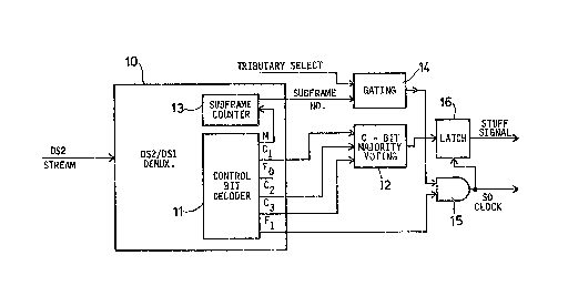
Figure 6 illustrates, in diagrammatic form, suitable
monitoring circuitry for extracting from a DS2 stream the
10 stuffing information relevant to a selected tributary, the
circuitry being arranged to output an S0 clock signal indi-
cative of stuffing opportunities relating to the tributary
and a stuff signal the logical value X of which indicates
the presence or absence of a stuff.
The Figure 6 circuitry is built around a DS2/DSl de-
multiplexer lO of standard form well known to persons
skilled in the relevant art. The demultiplexer lO includes
a control bit decoder ll operative once the demultiplex has
correctly locked onto the framing structure of the DS2
20 stream, to output signals indicative of the state of each
control bit within each subframe.
The three stuffing control bits Cl, C2, C3 are
fed from the decoder ll to a C-bit majority voting circuit
12 which outputs a single signal representative of the pre-
25 dominant value of the three control bits in each subframe.
The M bit output of the decoder ll is fed to a subframecounter 13 which determines from the received sequence of M
bits, the number of the current subframe. This subframe
number is output to a gating circuit 14 which is also fed
30 with the number of the tributary the jitter of which it is
desired to measure. The circuit 14 is arranged to output
an enable signal during each subframe that contains stuffing
information relevant to the selected tributary.
The enable signal from the circuit 14 is fed to an AND
35 gate 15 together with the Fl bit output of the decoder ll
whereby to produce a clock signal at the M-frame rate which
~tj9L~3
is synchronised with Fl bits of the subframe carrying
stuEfing information relevant to the selected tributary;
this clock signal can be considered as indicative of the
occurrence of stuffing opportunities for the selected
tributary and thus constitutes the S0 clock signal.
The S0 clock signal is used to clock a latch 16 fed
with the output of the C-bit majority voting circuit 12.
The output of the latch 16 constitutes the required stuff
signal with a logic value X which provides an indication of
whether or not the latest stuffing opportunity has been used
to stuff the selected tributary (X having a value of '1' if
a stuff has occurred and '0' if no stuff has beer. effected).
The S0 clock signal and the stuff signal constitute the
output signals of the Figure 6 monitoring circuitry and
these signals are fed to a signal processing arrangement
(Figure 7) which is operative to determine a current value
of jitter for the selected DSl tributary.
The Figure 7 signal processing arrangement is built
around two Intel 8031 8-bit microprocessors 20 and 21 which
together with associated circuitry and programs form
respective processors designated JMU and SMU respectively.
As will be more fully described hereinafter, the JMU proces-
sor is arranged to calculate a current stuffing ratio value
Sl in accordance with relationship (3) above while the SMU
processor is arranged to utilise relationship (4) to
calculate a running digital sum (RDsum) representative of
the current jitter value Jl (the SMU processor reading in
the current stuffing ratio value from the JMU processor
during each determination of Jl). The use of the two
processors JMU and SMU is required due to the tight time
constraints placed on the system by having the stuffing
ratio and current jitter value updated following every stuf-
fing opportunity.
Referring to Figure 7 in detail, the microprocessor 20,
21 of each of the processors JMU and SMU, is clocked at 15
MHz (by a common clock) and operates under the control of
:
16
assembly-language programs stored in a ROM memory 22. The
data lines of the memory 22 are connected to port P0 of the
microprocessor while the memory address lines are controlled
from the microprocessor ports P0 and P2. As is standard,
5 the low address byte and the data are multiplexed on port P0
with the low address being latched into a latch 23 under the
control of an ALE (address latch enable) signal output by
the microprocessor 20, 21.
The stuff signal from the ~igure 6 monitoring circuitry
lO is fed to an input T0 of each microprocessor 20, 21 while
the S0 clock signal is fed to a high-priority interrupt
input INT0 of the microprocessor 20 (the JMU processor). An
output Tl of the SMU microprocessor 21 is connected to a
low-priority interrupt input INTl of the JMU microprocessor
15 20 while an output Tl of the JMU microprocessor 20 is con-
nected to a high-priority interrupt input INT0 of the SMU
microprocessor 21. These connections permit the micropro-
cessors to demand information from each other, the actual
information being passed via a bus 24 interconnecting the
20 microprocessor ports Pl.
The ports P0 and Pl of the SMU microprocessor 21 also
serve for the output of the current running digital sum
value (the current jitter value) to a digital-to-analog
converter 25, the data output on ports P0 and Pl being first
25 latched into latches 26. In fact, only five bits of the
output of port P0 are used and of these only the two most
significant bits relate to the running digital sum, the
remaining three bits being used to select one of three poss-
ible output ranges. This range or scale selection is
30 effected by the selective enabling of one of three analog
switches (block 27), each switch being associated with a
respective amplifier 28 connected between the output of the
DAC converter 25 and an analog jitter output 29; the ampli-
fiers 28 have different gains corresponding to the desired
35 output scale.
Control of the JMU and SM~ microprocessors 20, 21 ~for
~2~ 3
17
example, to set the value of M in relationships (3) and (4)
above and for scale selection) is effected via shared trans-
mit and receive lines 30,31 which serve to provide unbal-
anced normal class communication. In the present example,
the lines 30, 31 serve to communicate the microprocessors
20, 21 with a central control microprocessor (not shown as
it forms no part of the present invention).
It will be appreciated that in Figure 7 various of the
microprocessor control lines such as the read/write lines
lO have been omitted for reasons of clarity; the functions of
such lines are, of course, well understood by persons
skilled in the relevant art.
The JMV nd SMU processors are arranged to run a number
of programs or routines, the most important of which are
15 interrupt initiated while the remainder are background
routines. Table 1 lists the routines run by the processors.
The three most important routines JITMEAS, SRSEND, and
RDSUM, are linked in~a sequence that is set running by each
S0 clock pulse, the routines JITMEAS and SRSEND being car-
20 ried out by the JMU processor to calculate the current stu-f-
fing ratio and pass this value to the SMU processor, and the
routine RDSUM being carried out by the SMU processor to
calculate the current jitter value as represented by the
running digital sum RDsum. The routine JITMEAS also serves
25 to keep a 'hits count' (that is, a count of the number of
times the jitter value exceeds a preset threshold) while the
routine SRSEND additionally determines the maximum and
minimum jitter values over a gating period determined by the
value of M set for implementing relationships (3) and (4).
The passing of particular values of adjustable
measurement parameters to the two processors over the line
31 is handled by respective routines CDENTER, the parameters
concerned being the parameter M, the output scale provided
by DAC 25 and amplifiers 28, and the 'hits' threshold. The
3sroutine CDENTER for the SMU microprocessor 21 is interrupt
driven via the low priority interrupt of the microprocessor
94~;~
18
~ . . .~
~ I .
E ~J l C O
E~ ~ ~I C ~ JJ ~ 0 ~
0 ~ ~ C v ~ ~ C CV~ u~ 0 ~u~ O C
a v ~ o.~ v ~ o
D~ ~ C ~ _I a~ E ~ E ~ V ~ V ~
o ~ cu~ C ~ V
U~ . ~ L~ C In ~
:~ a, u, u^) 0 ~ ~q a) 0 3 a~ ~- aJ ~ ~ V
r~J V 0 :~ ~ C ~ U~ V ~
~: ~ C ~ ~ o O ~ o~ C
~ ~ :~ . JJ~ O~
v~ ~ ~n ~ c _~ ~ n JJ E ~ v ~ v ~, a~ ~ v
t~ Q c ~ O ~ C c ~~ 0 ~ E
_l ~ ~ V-~ . O ~ O ~ ~C O
C O ~ v o ~E O ~ O Q~ Q. ~ D v 0 3 0 ~ a3 V
tn ~ O tn
~ :Z E~
a a o ~ ,
c~;
I ~E C
o
C ~ ~ C~
v ~ a~ ~ ~ c I E ~q O
u~ . C ~ ~ ~ C
h~ . .,1 o E _~ _1 . v ~ O
X ~ ~ ~i C V V ~
a~ ~ ~:v~c ~ ~ o ~ v ~ a~ c al~ ~ .o c
c ~ / E C ~ o v ~ u~ ~ v C a~ 0 ~5; O
E~ c v E v ~ C ~ ~ E~ a) E . v O E v ~ r4
0 0- ~ .,.~ ~ ~ v
a~ ~ 4~ .X ~ ~ ~-n ~ ~
::~ ~J ~ oq ~ o ::1 c v 07 c ~ a\ o 0 ~ ~ v
~ u v v ,~ ~ ~ ~I v _I ta v u~
:E ~ Ll O ~ / E L~ E ~ O ~ o ~ ~ ~ ~ v L~ c
:: v ,~ o ~ 0-~ v ,/ ~ v ~ ~
~, v tJ~ V CJ v C 0 Ll ~ v E ~ ~ ~ O. v v E
_I c c o ~ ~ ~ v a~ c c " - ~ v V c OQ ~l E
1~ rl O ~ ~ C a~ r1 ~ o ~u O ~ ~ c o
~ a ~ ~ J o ~ o t~ o Q. o ,~ o E E1 ~ V
3 a ~ o
E: Z Z E~ E~
E~ ~; C~ ~ ~
~a ~ ~ ~n
- o ' ''
E~
z v
n
E~ ~ u~ Z
~ ~ ~ - ~ ~ ~ u~
K Z ~ Z Z O ~a
~ 0 :~
X C~
C-~ ~ ~ E~
~1 0 i-l Ll O O ~> ~
~; ~ O
a~ ~
__, _ . .. _ .
. ~
`
` ~:
19
21; however, for the JMU microprocessor, a polling technique
must be used since the microprocessor has only two interrupt
levels both already in use.
The routines CDENTER are also used to output on line 30
digital jitter measurement results including the 'hit count'
and peak-to-peak jitter values.
As background routines, the JMU and SMU are arranged to
run main background routines MCONTROL responsible (a) for
checking that the measured jitter value has settled to a
10 stable level, (b) for effecting certain less important
jitter parameter measurements, (c) for calling the CDENTER
routines when measurement results are to be output on line
30, and (d) for initiating self-test and calibration rou-
tines SELFTEST and CLBRT.
So far as the jitter measurement process of the present
invention is concerned, the routines of major relevance are,
of course, JITMEAS, SRSEND and RDSUM; however, the portion
of the MCONTROL routines that checks whether the measured
jitter signal mean has settled to an acceptable value (the
20 LOCK condition) is also of interest. The structure of
these latter routines will be now described with reference
to the flow charts of Figures 8 and 9. As for the remain
ing routines, they can be implemented in a wide variety of
ways to suit particular circumstances and the writing of
25 suitable routines is well within the capability of persons
skilled in the relevant art; accordingly, these routines
will not be further described in detail herein.
The interworking of the JMU and SMU processors in
executing the routines JITMEAS, SRSEND and RDMEAS is illus-
30 trated in Figure 8. Upon an SO clock pulse being receivedby the JMU microprocessor 20 at its input INTO, the JMU
processor enters an interrupt process which installs the
routine JITMEAS. The first action of this routine is to
pass a request to the SMU processor for the current value of
35 the running digital sum RDsum, this request being routed via
the JMU microprocessor output Tl and the SMU microprocessor
input INTO. The request from the JMU processor causes the
SMU processor to install the RDMEAS routine. The first
operation performed by the RDMEAS routine is to pass the
currently stored value of RDsum to the JMU processor via the
5 bus 24 (microprocessor ports Pl).
On receipt of the RDsum value, the JMU processor, under
the control of the JITMEAS routine, calculates a new value
for the stuffing ratio in accordance with relationship (3)
given above and the currently set value of M; during this
lO process, the JMU processor reads in the current logical
value X of the stuff signal fed to the input TO of the
microprocessor 20. After calculating the new stuffing
ratio value, the JMU processor next checks whether the
latest RDsum value read in from the SMU processor has taken
15 RDsum over the current 'hits' threshold; if this is the
case, a further 'hit' is recorded (note that a 'hit' is
defined in terms of a transition over the threshold rather
than in terms of how long the threshold is exceeded). Once
the 'hits' count has been updated, the JMU processor
20 terminates the JITMEAS routine and returns to the background
routine that was being executed immediately prior to receipt
of the last preceding SO clock pulse.
With respect to the RDMEAS routine running on the SMU
processor, after this routine has passed the RDsum value to
25 the JMU processor, it sets about determining a new value of
RDsum in accordance with relationship (4) above and using
the currently set value of M and the current value X of the
shift-signal. In fact, depending on the value of M, the
detailed manner of implementing relationship (4) may be
30 varied to minimise the bit shifting and other operations
used in the calculation process. Furthermore, the RDsum
calculation is carried out in such a manner that the
stuffing ratio value is only required towards the end of the
calculation process whereby to ensure that the JMU processor
35 has finished calculatiny a new stuffing ratio value before
this value is required by the RDMEAS routine running on the
~; .
:
. .
,'; '
SMU processor.
- The actual request for the new stuffing ratio value is
made by the SMU processor to the JMU processor via the INTl
interrupt of the microprocessor 20 and initiates the SRSEND
routine in the JMU processor. The first operation of this
latter routine is, of course, to pass the latest stuffing
ratio value (via the microprocessor ports Pl and the bus 24~
to the SMU processor which thereupon completes its RDsum
calculation and outputs the new RDsum value, via port Pl of
the microprocessor 21, to the DAC 25 as the current jitter
value. After outputting the current RDsum value, the
RDMEAS routine terminates and the SMU processor returns to
its background routine.
Meanwhile the SRSEND routine, after overseeing the
transfer of the current stuffing ratio value to the JMU
processor, causes the JMU processor to update the stored
maximum and minimum jitter values if so required (note that
this updating is not carried out using the latest RDsum
value calculated by the SMU processor, but rather, the RDsum
value passed to the JMU processor during the JITMEAS
routine). The SRSEND routine is also arranged to pass the
maximum and minimum jitter values to a buffer area, for sub-
sequent access by the JMU MCONTROL routine, if this latter
routine has previously set a corresponding flag; this flag
is, of course, cleared by the SRSEND routine upon passing
the ma~imum and minimum values to the buffer area. There-
after, the SRSEND routine terminates and the JMU processor
returns to its background routine.
The JMU and SMU processors now continue carrying out
their background routines until the next SO clock pulse
triggers the whole process again.
With respect to the transfer of the stuffing ratio and
RDsum between the microprocessors 20,21 during the routines
JITMEAS, RDMEAS and SRSEND, it is to be noted that for
reasons of time efficiency, these transfers are not carried
out using handshaking routines.
~ 3
Instead, adequate coordination between the micropro-
cessors is achieved by utilising the fact that the time
taken to enter into an interrupt service routine has known
maximum and minimum limits (in terms of machine cycles).
More particularly, the microprocessor that wishes to be
passed data initiates a data request by interrupting the
other processor; this other processor takes, in the present
case, 3 to 5 machine cycles to enter the appropriate
interrupt ro~tine (routine RDMEAS for the SMU processor when
the RDsum is requested by the JMU processor and SRSEND for
the JMU processor when the stuffing ratio is requested by
the SMU processor). Immediately the microprocessor which
is to send data has entered the appropriate interrupt
routine, it transfers the first data byte to the relevant
output port (in this case, port Pl) and holds it there for
Eive machine cycles.
As a result, the requesting microprocessor can be
certain that regardless of whether the sending micropro-
cessor has taken 3, 4 or 5 cycles to enter its interrupt
service routine, the first byte of the required data will be
present during three particular machine cycles following its
request for data (these three cycles corresponding to the
last three of the five for which the data is output in the
case where only three machine cycles are taken to implement
the interrupt request, and the first three of the five where
five machine cycles are taken). The requesting micropro-
cessor is arranged to read the data in the second of the
three machine cycles for which the data is certainly
present.
Second and third bytes of data can, if required, be
transferred in a similar manner with each byte being output
for five machine cycles by the sending microprocessor.
It will be appreciated that although with different
microprocessors to that described, the limits of variation
in the time taken to respond to an interrupt request may be
different, the foregoing data transfer method can still be
. . ' , .
63
used provided that the data is output for a period suffi-
cient to ensure that the data is present during at least one
common machine cycle (with respect to the time of request)
for the two limiting cases of response time.
As already mentioned, provision is made for setting
different values of the averaging parameter M for use in
evaluation of relationships (3) and (4) by the JMU and SMU
processors (it being recalled that in the present arrange-
ment the quantity N in relationship (4) is made equal to M).
In particular, four different values (designated in
increasing order of magnitude, M0, Ml, M2 and M3) can be
selected via the controlling central microprocessor and the
serial link constituted by the lines 30,31. The value of M
selected will affect operation of the jitter measurement
apparatus in two main ways, namely:
(a) the greater the selected value of M, the lower the
minimum frequency of jitter detectable - this
follows from relat~ionship (3) above;
(b) the greater the selected value of M; the longer
the settling time of the RDsum (jitter Jl) mean
value to an acceptable level following start-up or
a disturbance - this follows from relationship
(4).
The settling of the RDsum mean to an acceptable level (that
is, to within an acceptable distance of the required mean
value K) is referred to as 'lock-up' and the actual time
taken to achieve this condition will, of course, not be
fixed for each value of M but will depend on the discrep-
ancies between the currently held value for S and J (~Dsum)
and the actual values of the stuffing ratio and jitter.
Situations in which the measurement process may be out of
lock include following initial start-up, following a major
change in a tributary parameter such as a change in
frequency, or following a change in output scale (as this
may result in a previously acceptable discrepancy be~ween
actual and required RDsum mean becoming unacceptable).
24
Table 7 gives typical values for the parameter M
together with their associated lowest jitter frequencies
measurable and comparative times to lock-up (the latter
times being measured under the same conditions).
TABLE 2
Comparative
Averaging ValueMin. Jitter Lock-up
Parameter of MFrequency Times
MO 29 lO Hz ls
Ml 215 0.16 Hz 56s
M2 2l7 0.04 Hz 4mins 30s
M3 223 0.6 mHz 7hrs
If it is desired to make accurate quantative jitter
measurements, then such measurements should be made in the
'in-lock' condition and not prior to lock-up (the 'out-of
lock' condition). Accordingly, as part oE their background
routines MCONTROL, the JMU and SMU processors are each
arranged to determine the current state of lock and to set
an internal bit appropri~tely (this LOCK bit is given a
value 'l' when the system is out of lock).
The section of the MCONTROL routines relevant to Lock
state determination is depicted in flow chart form in Figure
9. In general terms, lock state determination is carried
out on the empirical basis that once the value of RDsum has
fallen within certain limits determined by the set output
scale, then the mean value of RDsum will settle to an
acceptable level within an empirically-determined time-out
period measured as a number of stuffing opportunities
(this timeout period being, of course, dependent on the
current value of M set). Thus, after an initial check
(block 30) whether a new value of M has been requested by
the central control processor (for the present, this will be
assumed not to be the case), the JMU/SMU processor checks
(block 31) whether, for the set output scale, the current
RDsum value is within predetermined limits. If the RDsum
value is not within the predetermined limits, then the LOCX
'' ~., ,'
'~
i3
bit is set to '1' (out of lock) and a count SOCOUNT of
stuffing opportunities is cleared (see block 32); thereafter
the routine loops back to block 30.
In fact, where the current set value of the averaging
parameter is M3, then large values of RDsum may be expected
regardless of the scale set so that in this case (M3 set) a
special set of limits can advantageously be used in the
block 31 test, this set o~ limits being the same for all
output scale settings (the set-scale-dependent limit testing
remaining unchanged where the averaging parameter has a
value of MO, Ml or M2).
The routine will loop round blocks 30, 31 and 32 unless
and until the value of RDsum is within the appropriate set
of limits whereupon a check is made (block 33) as to whether
the LOCK bit is set. If the LOCK bit is set, this indicates
that the system is half-way through the lockup process, that
is, it has passed the limit test but the time-out period had
not, at its last testing, fully elapsed. If the LOCK bit
is not set, this indicates that the system was previously in
lock and, following the test in block 31, can still be
considered to be so; in this case, the section of routine
illustrated in Figure 9 is exited.
In cases where the Lock bit is found to be set, the
routine next proceeds to check (block 34) whether in fact
the time-out period has now elapsed. As previously noted,
the duration of the time-out period is dependent on the
value of M set and is measured in terms of stuffing oppor
tunities, that is, by the count SOCOUNT. This latter count
is independently kept by both processors JMU and SMU, the
JMU SOCOUNT being, for example, incremented each time the
JMU enters its JITMEAS routine and the SMU SOCOUNT being,
for e~ample, incremented each time the SMU enters its RDMEAS
routine. Since SOCOUNT is cleared in block 32 when RDsum
is found to be outside the limits tested by block 31, the
value of SOCOUNT tested in block 3~ will be a measure of the
time elapsed since RDsum first fell within the appropriate
26
limits.
If the time-out period appropriate to the current value
of M has not elapsed, the routine loops back from block 34
to block 30. If however, the time-out period has elapsed
then, disregarding for the moment block 35, the LOCK bit is
reset (block 36) as the measurement process is now locked-
up; thereafter the section of routine shown in Figure 9 is
exited.
Returning now to a consideration of the procedure
adopted if the test carried out in block 30 indicates that a
new value of M has been requested, a comparison is first
made between the desired value of M and that currently set
(block 37). If these values are equal, then the routine
proceeds directly to block 31. If the desired value of M is
less than the current value (for example, the desired value
is Ml and the current value M3), then the current value is
set straight to the desired value (block 38), it being noted
that if the measurement process were previously in lock,
decreasing the value of M will generally not alter the lock
state; since the measurement process may not have been in
lock when the new value of M was requested, the SOCOUNT is
cleared (block ~8) so that the subsequent lock-up time-out
process will be correctly carried out.
If the desired value of M is greater than the current
value (for example, the desired value is M3 and the current
value is Ml), then, of course, it would be possible simply
to change the current value to the desired value and proceed
accordingly. It should be noted that the fact that the
measurement process was in lock prior to the increase in
value of M is no guarantee that this will still be so after
the increase and, accordingly, the LOCK bit must be set and
the SOCOUNT cleared. The foregoing procedure is, in fact,
the one adopted for the case where the desired value of M is
only one greater than the current value (see block 39). In
cases where the difference between the desired and current
values is greater than one, a modified proceduee is adopted
; ;...:~;. ,.,...: . .:
:.: .
~ ' ' '
:
27
with a view to speeding up the settling process, that is, to
reduce the overall time to lock-up (it being recalled that
the higher the value of M, the longer the lock-up time).
In particular, where the desired M exceeds the current M by
more than one increment, then the desired M is approached by
stepping up the current value of M one increment, achieving
lock-up with the ne~ current M, incrementing M again,
achieving lock-up and so on until the current M is equal to
the desired M. This process achieves lock-up at the
desired value of M in a shorter time than simply directly
setting the current value of M to the desired M, due to the
~act that the settling time constant is not at the high
level corresponding to the desired M for the whole of the
settling process but is at a lesser value for a portion of
this process.
In Figure 9, this incremental procedure is achieved by
incrementing the current M in block 39 and then once lock-up
is achieved (block 34), testing whether the current value of
M is that desired; if this is not the case, then M is incre-
mented again (block 40) and the routine is looped back toachieve lock-up with the new value of M, this procedure
being repeated until the current and desired values of M are
equal.
The jitter measurement apparatus described with refer-
ence to Figures 6 to 9 can, of course, not only be used to
measure the jitter of a selected DSl tributary in a DSl
stream, but can also, with the addition of a DS3/DS2 demul-
tiplexer, be used to measure jitter of a DSl tributary in a
DS3 stream (that is, a steeam made up of seven DS2 streams).
It will be appreciated by persons skilled in the signal
processing art that the JMU and SMU processors can be
considered as forming a digital filter receiving the stuff
signal as input and clocked by the S0 clock signal. The
Z-transform transfer function of this digital filter can be
readily derived from relationships (3) and (4) above on the
basis that:
;9~63
28
SO = SlZ-l
Jo = Jlz-l
In particular, for a constant value of M, the transfer
function takes the form
J(z) = X(Z).(M-l)(Z_Z2) (S)
M(Z-(M-l)/M)2
where:
J(Z) is the output of the digital filter and
represents the value of the jitter signal;
and
X(Z) is the value of the stuff signal.
If the output of the filter is expressed in terms of
quantity RDsum rather than J (J = RDsum - X), then a further
term needs to be added to the right-hand side of relation-
ship (5), this term being:
KZ
M(Z - (M-l)/M)
Of course, in cases where M~N in relationship (3)
and (4), the above ~-transform transfer functions will need
to be modified.
: