Note: Descriptions are shown in the official language in which they were submitted.
--1--
e3c~1p~
Sa~uri~y ~ag ~c~lva~ion_~y~kem
Thi~ i~vention relate~ to 01~ctroni~ sy~t~m~ in whlch
resonant circuit i~ dat~ctsd whan brought in~o proximity
to c~rtain el~troni¢ egu~p~nt, Such sy~tQ~ are
utilized p~rticularly for ~ecurity purpose~, ~uch as
~hopli~ting prQvention, but are not limitQd to ~uch
appllcation~.
In thair application to shopli~tin~ prevention, such
10 sy~tem~ includ~ equipment ~or e~ta~lishing a
radio-~raguency ~RF) ~ield at th~ exit o~, say, a retail
atore. Attache~ to each article o~ merchandise in the
~tore which i~ to be prote¢ted ~rom shopli~ting is a tag
bearlng the r~30nant circuit, which i~ con~tructed to
15 hav~ a re~onance ~requency within thQ rango o~
~r~yuenaie~ o~ the ~ield. When ths article i~ properly
paid ~or, the clerk at tha chack-out counter either
removes this tag, or el~e render~ it e~ctivGly inactivQ
by the application o~ a ~hlelding label. Otherwise, the
20 sy0tem ~n~e~ the pa3sagQ o~ the 5till-actlv9 tag through
ths RF ~ield upon axiting and glve~ an alarm. For
con~enient ro~erencs, ~uch ~y~tem~ are herea~ter re~erred
to a~ ~loctronia artiale ~urveillance, or EAS ~y~tems.
The re~onant circuit borne by eaah tag u~ed with such
25 E~ ~y~to~ a m~ltilayer ~txuatura, having a
dielectrlc ~ubatrate, on op~o~lte ~ide~ o~ which are
conduativ~ l~yor~ ~o ~hape~ a~ to d~in~ a capacitor and
an lnductor whi¢h ~oopar~ta to provldo tho circuit
re~onant at th~ de~ired ~r~quency.
~0 It h3s pr~vlously been proposnd to xender ~uch a tag
inactivo by ~ ~ore "elegant" technigue than that o~
phy~ical removal, or shiolding. That improved technique
` 3~
,
': : ' ;,. .. . .
.' . ' ' ' ~ '': ' ' '' '
~2~ 35
2--
i~ di~closed in U.S. Patent No. 4,498,076, i~ued
February 5, 1985, in th~ na~ o~ Georg~ J. Lich~blau. It;
involves providing th~ tag ~t~el~ with a local$zed region
where th~ s~ac:ing betw~en conductor~ oa oppo~ite side~ o~
5 tha dielectric ~ub~trat~ i~ reduced, e . g. by an
indentation. Il: Iurther lnvolve~ providlng el~ctronio
equipm~n~ whlch sen~ the pre~enc~ o~ a tag (by a
proce~ g~n~rally ~imila~ to that used by the EAS system)
and thereupon e~tabli~he~ a RF ~ield at ~requencie~ which
10 includo the r~sonant ~requency o~ the tag and at a
~uî~ic:i0nt power level that breakdown occurs be~ween
conductors on oppo~ite ~ide~ o~ the diel~ctric. ~hi~
"dea¢tivatQel' th~ tag and do~s ~o by purely elsctronic
mean~.
In ord~r to prav2rlt con~u~ion o~ t~ betwe~n the EAS
~ystem prevloualy de~¢rib~d, and tha ~l~ctronic equipment
u~od to sen3a and then deactivat2 th~ resonant
circuit-bearing tag~, thQ latt~r i~ r~err3d to herein as
an elQctronic d~activation, or ED sy~thm.
Deactivation using an ED system, in accordance with
~aid PatQnt N~. 4,498,076, i8 a ~ound concept. However,
th~re ara matt0r~ o~ practical implementation which msrit
con~ideration beyond what i~ given to them in said
Pat~nt.
The~e include ~u¢h item~ a~ how to avert po~ible
inter~erenc3 botween nearby ED systems, or batween ED and
E~ 3y~tem~, how to provida ~uitablo indlcation~ o~ ~ag
deactivation, and how to di~lpat~ tho relatively high RF
power whlah i~ d2veloped by the ED ay~tem during
30 deactlvation.
Ik is an ob~ect o~ th~ pre~t invention to deal with
the matt~rs not~d abova.
Thi~ and othor ob~act3 which will appear are
accompli~hed in accordanco with the pr~enk invention a~
35 ~ollow~.
.. . .
'
' ' ,, :- ~
~i$73~
-2a~ 723~6-1
This invention relates to a system for deactivating a
tag which bears a resonant clrcuit made of conductors on opposite
sides of a dielectric substrate by applying to said circuit
sufficient RF power at its resonant frequency to disable said
circuit through breakdown between said conductors~ the improvement
which comprises:
means for detecting the presence of said tag near said
system;
means for responding to said detection to initiate a tag
presence signal, said initiating means including means :Eor
detecting the presence of said tag near a pad housing an RF
transmit antenna and an RF receive antenna;
means for sensing the cessation of said detection due to
disablement of said circuit by said RF power;
means for extending the duration of said tag presence
si.gnal by a predetermined period of time beyond said sensing of
cessation of detection; and
means for responding to sa:id detection to produce a
signal capable o:E inhibitlny the detection of the presence of a
tag near another declctivating sy~tem.
. . ... .
:
73~
-3-
Coupling in provided between any yiven ED ~ystem and
any other ~uch B~tem or any EAS sy~te~ which is near
enough to ~reat~ ~utual int~r~erencQ~ Thi~ coupling iB
used to inhiblt the tag det~ction ~unction o~ the~e other
5 ~y8te~8~ whsnev~r a particular ED ~yst~m i~ operating at
it~ his~h po~ r, or d~aati-rating l~v~ hil~ togethBr
w~.th slaving o~ th~ ~F tran~mi~ion~ ~ro~ all the~e
~y~tem~ pr~vent~ po~ibl~ interferenca b~tw~en the~.
D~a~tivation i~ indicat~d by the onding o~ an alert
10 ~ignal which i~ started when a tag i~ det~cted by mean~
Or ~he ED ~yste~. Moreo~erl for rQason~ whlch will
app~ar, th~ alQrt ~ignal i~ deliberately extendad by a
predetermined int~rval beyond the time at which tag
detection cea~e.
A3 ~or power di~ipation, mean~ are provided ~or
accompllshing thl~ at a location remote ~rom that at
which tha t~g ds~ctivation itsel~ i~ par~ormed.
For ~urther detail3, ra~0renca i~ made to thQ
di~cu~ion whlch ~ollow~, in light o~ th~ accompanying
20 drawing~ whex~in: .
Figure 1 ~hows, in ~impli~ied, diagrammatic ~orm, the
ma~or ale~nt~ and layout o~ an ambodiment o~ the
inv2ntiont and
Figur~ 2 ~hows, in block diagram ~orm, the electronic
25 component~ o~ ~uch an embodiment.
The ~am~ re~exence numbors de~ignate similar pa~t~ in
the di~ran~ ~igura~.
Re~erring to Figura 1, thi~ ~how~ in i30metrlc view ~he
cho~k-out area o~ a r3tall ~tora, 3uch a~ a drug ~tore,
30 Por example.
~ rhe ~tore sxit opening i~ de~ignated by re~eronoe
numeral 10~ Near that exit is the aheak-out aounter 11,
vlewed in Figure 1 Rrom th~ ~ide on which the clerk
stand~ while ch~¢king out m~rchandise. ~he cu~tomar, o~
35 cour~e, 3tand~ on the oppo~lte side o~ counter 11 and
. ~ , . ~ '
. ~,.. . . .
.. . .
., " .
plac~ tha ~rchandise to b~ checked out on the
counter~o~ 12. Also on countsrtsp 12 i~ ths cash
regi~tar 13 and a unit 14, which ~orm8 part o~ the ~D
sy~te~ ~mbodying th~ pr~ent lnvention. Ano~hex part Or
that ED ~y~t~, na~ely a cabin~t 15, i9 positioned on a
sh~l~ 16 b~low th~ countertop 12, and i9 ConneCtQd to
unit 14 by c~bling 17. N~r the ~xit Qnd o~ checkout
counter 11 and al~o ad~aoant to exit 10, th~re are
po~ition~d antanna3 18 and 19, ~orminy part o~ the EAS
10 sy~te~ with which th~ ED ByStem cooperat~.
In the version o~ all thi~ equipment which conRtitute~
tho embodiment currently pre~Qrred by thi~ inventor, the
EAS 3yste~ o~ which antennas 18 and 19 ~orm a part i~ the
type which i~ ~old by Ch~ckpoint syatQm~ Inc., o~
15 Thoro~are, Now Jer82y, under tha modal designation
Checkpoint Mark III. Bri~ly, it compri~e~ an RF
transmitt~r, which i~ conventionally housed in a cabinet
mounted betw~en th2 vertical leg~ o~ ons o~ the EAS
antenna6, say antenna 18, ~hown in Figure 1, but too low
20 to be vi~ibl~ in ~lgure 1. Thi~ tran~mittar produces a
signal which recurrenkly ~weep~ through a ~reguency range
centered, ~ay, at 8.2MHz ~nd extending 0.8MHz above and
below that cent~r ~requency. This signal i8 radiatsd by
the tran~mit antonna 18 and pick~d up by receive antenna
29 19. The latter ia conne~t~d to a rec~ivar, hou~ed in a
cabinet (al80 not vislble in Figure 1) mountad between
the 12gs o~ EA8 antenna 19. That EA~ reaeiver 1~
con~tructed ~o a~ to proae3a the signal received ~rom
ant~nn~ 18 ln a m~nner which dateat~ the pre~naQ, in the
30 pa~ageway de~lned by antenna~ 18 and 19, o~ a re~onant
aircult tuned to ~ ~re~uency within the range o~ 3waep o~
th~ kran~mitter, ~.e. between 7.4 and g.OMHz. Upon
detect~on o~ such a re~onank cirduit, an alarm indication
1~ given. In thi~ manner, an attempt to remova an
35 artial3 o~ merchand~e wh~ch i~ protected by a tag
~2~
72386 1
bearing such a resonant circui~ will be detected and can then be
followed by the appropriate security measures.
The specific configuration used for antennas 18 and 19,
and the specific c~ircuitry to be used in conjun~tion ~herewith
does not constitute a part of the present invention and may,
furthermore, take any one of various well-known forms. However,
in the ~orm which this inventor currentl~ prefers, antennas 18 ancl
19 will have a con~iguration as disclosed in United States Patents
No. ~,243,980, issued January 6, 1981 and No. 4,251,308, issued
February 17, 1981. The receiver circuitry which cooperates with
antenna 19 wlll include means for processing the received signals
so as to determine whether a resonant circult- bearing tag is
present near the antennas 18, 19. This signal processing means
may also take varlou~ known forms, for example, those disclosed in
United States Patents No. 3,828,337, issued AucJust 6, 1974 and No.
4,117,466, issued September 26, 1978.
Turning now to the ED system of Fiyure 1, the countertop
unit 14 is preferably a ~lat "pad", made of non~conducting
makerial, such aæ a plastic. This pad l.s preferably about 16
lnches by 16 lnch~.s in area and about 3~4 lnch high. It enclo~es
transmitter and receiver antenna~, which may be generally ~imilar
to antennas 1~ ancl 19 o~ the EAS ~stem, but of course now much
reduced in dimenslons and located in the same horizontal plane as
the pad 14. This pacl also enclo6es a buzzer, the grille 14a of
which is visible in ~igure 1. It will be unclerstood that there
need not be such a cJrille and that the buzzer may be fully
enclosed in pad 14.
:
. ..
, ~.. : ."
:. ''" '::
~26~7~
Sa 72386-1
Cabinet 15 houses the electronic circuitry which ~or~s
part of the same ~D systemr For further description of
-. ,
~' ' : .. , ,, :
.. ': ''. :
~.
.. , :
3~
-6-
that electronia circuitry9 re~erenca i8 now mad~ to ~ts
illu3tration in the block diagram oP Figure 2. That
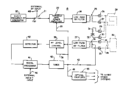
electronic circuitry compri~s a generator 20 of radio
frequency (RF~ ~ignal~ which i~ aontrolled ~o a~ to vaxy
it~ frequency o~ oper~tion recurr~ntly o~Qr a
prad~taE~in~d range, e.~. th~ same 7.4 to 9.O~Hz rangs as
in the EAS ~ystem. The output bf generator 20 may b~
~upplied via ~witch 21 to a power ampli~i~r 22, which i~
80 con~tructad that it gain (and resulting ou~put power)
10 may b~ varie~ b~twa~n a relatively lo~ and a relatively
high levQl by a control ~ignal supplied via connection
23. ~y m~an~ o~ ~witch 21, an RF slgnal ~imilar ~o that
fxo~ generator 20, but obtain~d in a manner explain~d
later, may ba u~ad in pl~c~ o~ that from generator 20
15 to drlv~ ampli~er 22. Th~ output signal ~rom ampli~ier
22 is 3upplied to a ~ilter 24, which supprQ~se~ high
~re~uency component~ abov~, say 12MH~, and from there via
coupling trans~orm~r 25 and shielded leads 26, 27, to the
trans~it antenn~ within pad 14 ~Figure 1). That transmit
20 antenna i3 ~hown dlagramatically in broken line~ in
Figure 2, wher~ it i9 d~ignated by re~erence numeral 28.
Al~o ~hown diagxammatically in bxoken lina~ in Figure 2
are the continuation~ o~ leade 26, 27 extending to
transmit ant~nna 28 via cabling 17 (Flgure 1).
Al~o conn~ct~d to th~ ~2me transmit antenna 28 within
pad 14 via cabling 17 (Figure l)ara shielded leads 29,
30. A~ ~hown di~grama~ically in broken line~, the~e
lead~ are connaated in parallol to lead~ 26, 27 at the
antenna connection~ within pad 14. Within cabinet 15,
30 they ara connected to a ~arie~ re~i~tanae-capacltance
airau.tt 31, 32 as ~hown ln Figure 2.
The reaeivor ~ntenna wlthin pad 14 ~Figure 1) i9 shown
diagramatiaally in broken ltn~s in Figure 2 designated by
re~er~nc~ numeral 33. It 1~ connected to the circui~ry
3S in cabinet 15 by ~hisld~d lead~ 34, 35, via cabling 17
' '
7~
-7-
and coupling transformQr 36. The signal~ ao received are
supplied to a low-pa~a ~ilt~r 37, similar to filter ~4.
Th~ output ~ignal ~rom that ~ilter 37 i8 ~upplied to a
circuit 38 which, under th~ control o~ a signal ~rom
conn~ction 39, is aapabl~ of passing th~ ~ignal wh~ch it
receive~ ~ro~ iilter 37 with eithar ralativ~ly low or
ralatively high attanuat~on. Tha signal ~rom thi~
control circuit 3~ up~lied to a detQctor 40 whlch
detect~ and prcduce~ a signal repr~entati~ o~ ths
10 modulation pre~ent on th~ R~ signal ~ro~ circuit 38. The
signal gro~ dst~ctor 40 i8 ~uppliad to a ~ignal
proc~s~ing circuit 41 which, in e~sence, utllize~ that
supplied ~lgnal to d~termine whather or not a re~onant
circu~t-bearing tag is present in the vicinity o~ the pad
15 14. Thi~ circuit 41 puto out a distinctiva output signal
wh~never it do~a determine that such a tag iB pregent~
Thl~ tag-repr~ntative output signal is suppli2d to a
timing circuit 42, which extend~ its duration by a
predetermined time interval.
The reeulting signal produced by timing circuit 42 ls
supplied, via previou~ly mentioned connections 23 and 39,
to power ampli~ier 22 and control circuit 39,
r~sp~ctively. In addition, thi~ ~ignal i~ supplied, via
conneatian 43, to the conter tap o~ the primary winding
25 o~ tr~ns~ormar 36, and vla connectlon 44, to tha
llght-emitting element~ o~ each o~ a plurallty o~ optical
coupler~ 45.
Thl~ ED ~y~tem ~una~lon~ a~ ~ollows.
Wh~n no re~onant aircuit-baaring tag i8 present in the
30 vicinity o~ pad 14 (Figur~ 1), tho powor ampli~ier 22
~Figure 2) i~ normally maintain2d at it~ relatively low
power l~v91 by tho control 3ign~1 supplled ~rom timing
clrauit 42 via connection a3. Thi~ power level may be
~uch a~ to provide an outpu~ power at tran~ormer 25 o~
35 approximataly 2 watt~ in a current ambodiment.
. ~ ,
3~
--8-
The aignal ~o transmitt~d via transmit antenna 2~ i~
rQc~ivsd by the receiY~ antenna 33 and ~uppli~d via
trans~ormar 3~ and ~ilter 37 to 1QV~1 control circult 38
5inc~ no tag i~ pr~nt in thi~ situation, th~ output
aignal auppliad ~ro~ ti~ing clrcuit 42 to control Gircuit
38 v~a connQction 39 will be such a3 ~o maintain that
control c~rauit in it~ low attenuatlon moda. The
received slgn~l pa~ed by circuit 38 wlll undergo RF
detection in circuit 40 and si~nal proc2~aing in circuit
10 41. Thia sig~al proce~ing will yleld an output fro~
circuit 41 which indicates th~ ab~ence o~ a re~onant
circuit-bearing tag ~ro~ the vicinity o~ pad 14. Timing
aircuit 42 will remain inactive in re~pona~ to such an
output aignal ~rom circuit 41, and will ~imply maintain
15 that output ~ignal ~or as long a~ it i8 pre~ent.
Now a~u~ that a cu~tomer staps up to th~ countQr 11
(Figure l), carrylng an article o~ merchandise which i9
protQcted by a re~onant circult-bearing tag, and which
that cu~tomer de3irsa to purchas~. It i~ now the duty o~
20 the chacX-out clerk to aee to it that thi~ article is
brought clo~0 ~nough to th~ pad 14, 90 that its presence
i~ detscted by thQ ED ~y3tem. Such dotection take~ place
when the re~onant circuit ~u~iciently distorte the
~igna~ tran~mitted ~rom and roceived back at pad 14 so
25 that tho ~ignal proces~ing circuitry 41 datermine~ that
the dl3tortion i9 attributable to a tag. When that takes
place, the outpuk ~ignal ~xom circuitry 41 undsrgoea a
di3tin¢tlv~ changa, e.g. ~rom a low to a high value.
Thi~ ahange i~ also re~leated at th~ output o~ timing
30 cirauit 42. ~ a rGsult, several other actions take
place withln tho ~D ~y~tem.
Via canneatlon 23, th~ gain o~ the power ampli~ler 22
i3 ral~ed to produca a transmitted ~ignal at the
proviou~ly mentioned relatively high power level. Thi~
35 may bs Or khe order o~ lO wat~s in a current embodiment.
,, ~
,
37~3~
g
Via connec~ion 39, the ~F level control circui~ 38 i~
changQd to it~ relatively high attenuation condition.
ThQ change ia prQfQrably ~uch that the output ~ignal ~rom
circuit 38 will r~ma~n at ~ub~tantially thQ same lavel
durinq the high-pow~r operation o~ ampli~i~r 22 a~ duæing
its low-pow~r opsration. In thi~ way, tha detector
circuitry 40 i~ ~roteotQd ~ro~ RF ~verload.
Via connection 43, th~ cQnter tap o~ tran~ormar 36,
and lead3 34, 35, th~ buæzer houssd in pad 14 i~
10 ac~uatad. Th~ buzz~r i8 shown dia~rammatic~lly in
broken line8, de~ignatad by refarence numeral 14b (Fi~ure
2). In practico, an ~F-i~olated dc path wlll be provided
to buzzer 14b.
Finally, via connectio~ 44, khe optlcal couplers 45 are
15 energized.
All o~ the condition~ de~cribed above will be
maintained rOr a~ long a~ 3ignal proce~sing circuitry 41
continua~ to detect a tag-representative received signal,
plu~ the additional predetarmined period o~ time
20 e~tabli~hed by timing circuit 42, a~ previously noted.
Ak th~ end o~ this total tlme period, the output ~ignal
~rom circult 42 will revert to it~ level corxesponding to
the absence o~ a re~onant circuit-bearing tag. This, in
turn, will cau~ pow~r ampli~ier 22 to revert to its
25 relatively low power ~od~, control circuit 38 to r~vert
to it5 low attenuation mode, the buzzer l~b to stop
operating, and the optical aouplers 45 to be deenargized.
~ha overall ED ~y~tem i~ then raady to re~pond to another
article o~ mer¢handlsa protected by a re~onant
30 alrcuit-b~arlng tag, in the same manner a3 described
above.
The purpo3e o~ providing timing circuit 42 ie as
~ollow~. ~rher~ are ciraum~tance~ under which the
d~tection o~ tha pr~0nce o~ a tag ln the viclnity o~ pad
35 14 occur~ ~o ~l~etlngly that an alerting ~ignal o~ the
3~;
--i0
-
same duration ~rom buzzar 14 could ea~ily be ovarlooked.
one ~uch clrcum~tanc~ ari~Qs i~ the article o~
mQrchandise to which tha tag .i~ attachsd i~ brought close
~o pad 14 only ~le8tingly and 1~ rQmov~d be~ore
dsactivation ~ollowing d~tsctlon can tak~ plac~. In many
rQta~l ~tores, m~rchand~ provided with tag~ only on
a ~electiv~, or ~ampla ba~i~; there~ora th~ check-out
clerk might then erronsou31y conclude that the particular
articl~ had not been tagged, and makQ no ~urth~r affort
10 to deactivate.
Anothsr 3uch circum~tanc~ might arls~ i~ deactivation
take~ placa very rapidly a~tsr detection. The clerk
might then concludQ, again erroneously, that thQ tag had
not yet been deacti~ated, and there~or~ continue ~utile
15 attempt~ to do ao.
Timing circuit 42 Pore~tall~ the~a problem~, by making
sure that an alert ~ign 1 o~ su~lcient duration will be
given ~o that it iB highly unlikely that it will not be
perceivsd. It has bean ~ound that a ~uitabl~ duration
20 ~or the tl~e p~riod by which timing clrcuit 42 extends
thi~ alert signal iB approximately 120 millisQconds.
It will be notsd that the output ~ignal ~rom timing
circuit 42 i~ ~upplied not only to buzzor 14b, where it
extend~ thn al~rt signal, but ~l~o to power ampli~ier 22,
25 attenuation control circuit 33, and optical coupler~ 45.
Thi~ 1~ not e~sentlal, because, onc~ tag detection
coa~e~, the~e okher element~ may all be allowad to raturn
to kheix ~oda~ corresponding to low-power output ~rom
ampli~er ~Z. How~var, lt i~ pre~erred to also extend
30 thair high power mode~ becau~e thi~ ~urther lnsure~ the
rellable determinatlon that ces~ation o~ dateation waa
due to deactivatlon o~ th~ tag.
Attention i~ invited to optlcal coupl~r~ 45. ~hesa may
have thelr resp~ative outputs connected to on~ or more
35 other ED ~y~tam~ or EAg sy~tems in the vicinlty o~ the
7~
11--
partlcular ED ~y~te~ shown ln Figur~ 1 and 2. These
output~ may bQ u~d to te~poraril~ inhibit th~ operation
of the~ other ~y~te~s, during the period~ that the
present ED sy~tam i3 ln it~ h~gh powar moda. That
prav~nt0 th~ op~ration o~ onQ ~uch systa~ in its h~gh
pow~r ~ode from cau~inq o~h~r nearby ~y~tæm~ to
erroAeously giv~ a tag pr~sencQ indication. That could
otherwi~e happ~n, i~ ED eguippad check-out coun~ers
and/or EAS equipped exit~ ars located clo~a to one
10 another. ~he sama inhibiting po~ibility ahould , o~
cour~e, also pr~vail ~or the particular ED ~y~tem ~hown
in the present ca~e. Thi~ i~ provided by terminal 46
(Figure 2~. Thi~ terminal may be used to apply an
external ~ignal, ~.g. ~rom another nearby ED ~ystem, to
15 i~hibit the ~ignal proce~clng circuitry 41 ~rom putting
out a ~ignal which repre~nt~ the presencQ o~ a tag in
the vicinity Or pad 14. By u~ing optical coupl~rs,
di~icultie~ which may be created by pr~viding d-c
conn3ctions betw~en ~y3tema aro avoided.
Attention i8 al~o dirQ~ted to sw~tch 21. When
connacted to tarminal 47 (a~ shown), the powor ampli~ier
22 r~ceiv~ it~ drivo ~ro~ generator 20. By changing the
3witch connection to terminal 48, it become~ possible to
utilize an extern~l RF signal to drlve the power
~5 ampli~ier 22. Such an external signal 1~ typically
derivad ~rom ~ nQarby EA~ sy~tem. The reason ~or using
0uch an ~xternal flrive ~ignal i5 a~ ~ollow~ the ED
sy~tem o~ Flgure~ 1 and 2 i3 permitt0d to oporate with
it~ own RF generator ~generator 20 in Figure 2) while a
30 nearby EA~ ~yat~m operate~ wlth its own RF generator,
then the lnt~ra~tlon batwe~n the re~lllting tran~mitt2d
signal~ ~an areate distortion~ Or the eiynal picked up by
the recaiv~ ant0nna o~ tha ED or th~ EA~ ~y~t0m which
will he ~i~ila~ to tho~o produced by the pr~s~nco o~ a
35 tag. Thi~ would th~n re~ult in ~ ~al~a alarm ~rom the ED
or EAS ~y~ . By driving both ~ystem~ ~1th tha same RF
signal, thi can ba avoided.
Attention i~ invlt~d to R-C natwork 31, 32 in Figure 2
~hi~ network, ~nd particularly it~ re~istlv~ component
5 31, i~ u~ed to dis~lpat~ relatively high power
generated whorl the ampli~iar 22 ~ in it~ high power
mod~. In thi~ ~ay, that power i~ di~ipat~d mainly
within cabinat 15, which c3n be con~eni~ntly e~uipp~d
with thQ apE~ropriatQ h~at ~inlc and cooling ~acllitiQ~,
10 rath~r than in p~d 14, which i8 pre~srably completely
anclo~ed and ~night there~or~ tend to ~Qco~e unde~irably
warm to the touch undar ~requent u~e.
In t:hQ vQr~ion which i~ currently pra~errQd by the
prQs~nt invontGr, th~ ED 0yste~ which 18 ill~strated in
15 Figure 1 and 2 i~ ba32d on the ~am~ operating principles
a3 tho EAS ~ysteDI prsvlou~ly de~crib2d- That i9, tha
rrequency o~ the tran~mitted signal i8 ~w~pt reourrently
through a rang~ o~ ~r~uoncis~ which includQs that at
which the tags to be deactivated are resonant. When such
20 a tag i~ brought near the pad 14, recurrent distortion~
ln the racelved 3ignal ocaur. The~e are utllized by the
signal proc~a~ing circuitry 41 to determine such tag
pre~ence, reaulting in th~ tranamisaion o~ aimilar
~wept-~requency ~ignal~, but at a hlgher power level.
25 ~i~ high~r pow~r level then producea breakdown between
conductor~ on oppo~ite eides o~ the tag 18 dlelactric
sub~trate, and thereby deactivation o~ the tag.
Not only ~ay tha ba~ic operating principl~s be the
~ame, but the ~me ~peci~la aircuitry may al~o be u~ed
30 ~or important ~lementa Or the ED ~y~tem a~ ~or tho EAS
~y~tem. In p~rtlcular, the ~ignal proce~ing aircuitry
41 o~ Figure 2 m~y be ~ub~tantially the aame a~ the
corre~ponding aircuitry in tho EAS ~yatem. Thua,
circuitry 41 may include the proc~ing circui~ry o~ U.S.
35 Patente No. 3,~28,337, and No. ~,117,466 prevloualy
~.~. - . - . , ~
3~3 21~7~
.
-13-
ntioned h~rein.
In all other re pQCt:e~, thel ele~nts ~hown in Figur~ 2
may tak~ any on~ o~ a nu~ber o~ co~v~nt~onal ~orms, and
ar~ there~ora not de crlb~d in ~urth~r d~t~il.
It wlll be understood th~t the ~atur~s o~ th~ pr~ent
in~entlon ~ not limit~d, in their application, to the
~paci~lc ~qulpmant de~arib~d with rer~r~ncQ to Figure~ 1
and 2 h~r~in, Ra~her, on~ or more o~ ~hQ~ featur~s may
be appli~d ~ a wid~ variety o~ other spsai~ic
10 ~hodi~ent~ in¢luding all thos~ de~ribed in thQ
above-~ntion~d U.S. Pat~nt No. 4,243,980. Accordlngly,
it i9 desired that th~ ~cop~ Or this lnvention be
delineated only by the appended claim
;,