Note: Descriptions are shown in the official language in which they were submitted.
1;~70ta~6
RADIO COMMUNICATION RECEIVER WITH
APPARATUS FOR ALTERING BIT RATE OF THE RECEIVER
Background of the Invention:
This invention relates to radio communication
receivers in general and particularly to receivers
that decode digital signals transmitted over radio
links to remote locations.
Such receivers can comprise selective call
receivers of the type commonly utilized in radio
paging systems. A selective call receiver is a
receiver that responds and alerts the user to calls
that are directed to it only and not generally to
all calls on a frequency or channel. Convention-
ally, such radios recognize messages being
transmitted to it by the particular address
information of the transmitted signals. Commonly
used address information signals include sequential
tone signals comprised of multiple kones, and
digitally encoded binary frequency shift keying
(FSK) signals.
Digital code receivers include decoders that
operate at approximately the bit rate of the
transmitted digital signal, and serve to compare the
signal patterns received from the transmitter with
the signal patterns assigned to the pager. All
digitally encoded pagers in use today are designed
-1-
35i~ti
to operate at particular predeterminecl bit rates.
For example, a receiver for a POCSAG system is
designed to operate at 512 bits per second (bps),
while a receiver for a Golay Sequential code (GSC)
system is designed to decode addresses at 300 bps.
A display pager in a Golay system decodes data
messages at 600 bps.
As a general principle, the lower the bit rate
of transmission the higher the sensitivity of the
paging receiver and thus the higher the reliability
regarding reception and decoding of the signal.
Conversely, as the transmitted signal bit rate is
increased the sensitivity of the receiver and
reliability and accuracy of reception and decoding
decreases. This is particularly pronounced in
fringe areas where the radio signals may be subject
to interference or fading.
In present selective call or radio paging
systems, the system transmission bit rate is
preselected to provide an acceptable level of
accuracy for reception of digitally coded signals.
Once this bit rate is chosen, the maximum of number
of radio addrasses of a given length that can be
transmitted during any time interval is therefore
determined.
System loading over a 24 hour period of a fully
loaded paging system such as may be found in major
metropolitan areas is illustrated in FIG. 6. In
this illustration, the system is operating at 100
per cent of full capacity during the day from 10:00
A.M. until 4:00 P.M. This means, that the trans-
mitter is transmitting at 100 per cent of its
through-put capacity during this 6 hour interval
during which the channel is fully loaded. New mes-
-2-
52~
sages placed in the system during this time interval
can encounter delays of up to 15 minutes as they are
queued, waiting their turn for transmission. If the
effective bit rate of transmitted signals in the
system could be increased during this time interval,
then the message through-put during these peak times
could be increased thereby reducing or eliminating
such queing delays. Conversely, during lull periods
if the bit rate of transmitted signals in the system
could be decreased, greater accuracy could be
achieved without affecting system through-put.
Summary of the Invention:
The radio communication receiver embodying the
present invention includes apparatus responsive to
transmitted signals for altering the bit rate of the
receiver for decoding incoming digital signals.
It is one object of the present invention to
provide a radio paging system in which the
signalling bit rate may be changed.
It is another object of the present invention
to provide a radio paging system in which the
signalling bit rate may be changed by the
transmission of special bit rate control signals.
It is yet another object of the present
invention to provide a radio paging receiver which
can adapt to change in the system bit rate.
It is still another object of the present
invention to provide a radio paging receiver in
which the post detection signal filtering is
adjusted in accordance with change in the signalling
bit rate to provide optimum receiver sensitivity.
It is yet another object of the present
invention to provide a flexible paging system in
-3
~.~705~6
which the signal bit rate used to transmit data can
be adjusted for just one message transmission or for
all transmissions.
These and other objects will be more clearly
defined in the following sections.
Brief Description of the Drawings
FIG. 1 is a graphic representation of a typical
radio communications system.
FIG. 2 is a block diagram of a rad.io
communication receiver in accordance with the
present invention and having an apparatus for
altering the bit rate of the receiver.
FIG. 3 is a combined block and schematic
diagram of the receiver of FIG. 2 showing circuit
details of certain blocks.
FIG. 4 is a block diagram of the programmable
divider of FIGS. 2 and 3.
FIG. 5A is a functional diagram of a micro-
computer utilized in the system incorporating the
present invention.
FIG. 5B is a functional diagram of another ROM
showing major modules for use with the microcomputer
of FIG. 5A.
FIG. 6 is a system loading chart for a heavily
loaded paging system.
FIGS. 7A and 7B comprise a descriptive diagram
for a conventional data encoding system.
FIGS. 8A, 8B and 8C comprise a descriptive
diagram for a first data encoding system, for the
preferred embodiments of the invention.
FIGS. 9A, 9B and 9C comprise a descriptive
diagram for a second data encoding system for the
preferred embodiment of the invention.
5~
FI~S. lOA, lOB and lOC comprise a descriptive
diagram for a third data encoding system for the
preferred embodiment of the invention.
FIGS. llA, llB and llC comprise a descriptive
diagram for a fourth data encoding system for the
preferred embodiment of the invention.
FIGS. 12A, 12B and 12C comprise a descriptive
diagram for a fifth data encoding system for the
preferred embodiments of the invention.
FIGS. 13A, 13B, 13C and 13D comprise a detailed
flowchart of the implementation of the preferred
embodiment of the invention utilizing the data
encoding system of FIGS. 8A-8C.
FIGS. 14A, 14B and 14C comprise a detailed
flowchart of the implementation of the preferred
embodiment of the invention utilizing the data
encoding system of FIGS. 9A-9C.
FIGS. 15A, 15B and 15C comprise a detailed
flowchart of the implementation of the preferred
embodiment of the invention utilizing the data
encoding system of FIGS. lOA-lOC.
FIGS. 16A, 16B and 16C comprise a detailed
flowchart of the implementation of the preferred
embodiment of the invention utilizing the data
encoding system of FIGS. llA-llC.
FIGS. 17A, 17B and 17C comprise a detailed
flowchart of the implementation of the preferred
embodiment of the invention utilizing the data
encoding system of FIGS. 12A-l2C.
Description of the Preferred Embodiment
Referring now by characters of reference to the
dr ~ings and first to FIG. 1, it will be understood
that the radio communication system 10 includes a
5~6
transmitter ll comprising transmitter means that
transmits signals from antenna 12 to a plurality of
selective call receivers such as tone only pagers 14
and/or display pagers 15. The tone only pagers 14
are receivers that provide a tone alert signal when
their address is received, they do not provide voice
or data messages. The display pagers 15, in
addition to generating an alert, include a display
for displaying numeric or alphanumeric messages.
Other types of selective call receivers such as tone
and voice pagers (not shown) which provide voice
messages can be utilized.
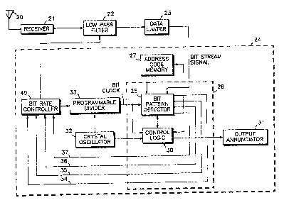
A block diagram of a radio communication
receiver having an apparatus for altering the bit
rate of the receiver, such as a tone only pager 14,
is shown in FIG. 2. The transmitted rf signal from
transmitter 11 is picked up at antenna 20 and
applied to a conventional receiver portion
designated 21, detected rf signals are passed
through low pass filter 22 and then through data
limiter 23 before supplying the digital signal to
the receiver control portion 24.
The digital signals are applied to a bit
pattern detector 25 of a microcomputer 26 where they
are compared with address codes that are stored in
an address code memory 27. Control logic 30
interfaces with the bit pattern detector 25 and the
address code memory 27 as well as an output
annunciator 31 which constitutes output signallinq
means. In a display pager such as that indicated at
15 in FIG. 1, the output annunciator 31 would
typically include an LCD for displaying numeric or
alphanumeric messages as well as a tone alert
generator as is used with the tone only pagers 14.
A crystal oscillator 32, constituting a refer-
ence oscillator, supplies timing signals to both the
control logic 30 and to a programmable divider 33,
constituting divider means. The bit pattern
detector 25 is connected as by lines 34-37 to a bit
rate controller 40 which is connected to both the
programmable divider 33 and low pass filter 22. The
circuitry of the bit rate controller 40 and low pass
filter 22 are shown in further detail in FIG. 3.
The bit rate controller 40 includes type D
flip-flops 41, 42, 43 and 44 connected to lines
34-37 respectively at their D inputsO Lines 34-37
are also connected to four inputs of an OR gate 45
which has its output connected to the clock C inputs
of flip-flops ~1-44. Whenever one of the lines
34-37 switches high, OR gate 45 clocks the D
flip-flops 41-44 thereby latching the output of the
bit pattern detector 25 on lines 34-37 into the bit
rate controller 40.
The bit rate controller 40 further includes
four output lines 51-54 which are connected to the Q
outputs of flip flops 41-44 respectively. Lines
51-54 are connected to both the low pass filter 22
and programmable divider 33. The pass band or
cutoff frequency of low pass filter 22 is determined
by the output of bit rate controller 40. This is
accomp~ished by using transistor switches 61-64 for
selecting the capacitance of the filter 22. Output
lines 51-54 are coupled through resistors 55-58 to
base connections of transistors 61-64 respectively.
Capacitors 65-68 are connected from the output of
low pass filter 22 to the collectors of transistor
61-64 respectively. The emitters of transistors
61-64 are each connected to ground. Connected
~x~s~
between the input and output of low pass filter 22
is a resistor 69.
In operation, a particular one of the tran-
sistors 61-64 is turned on causing its associated
capacitor to be ~actuated to determine the cut off
frequency of low pass filter 22. The connection of
bit rate controller 40 to the programmable divider
33 is shown in further detail in FIG. 4.
The crystal oscillator 32, which can be of
conventional design, provides an output signal on
line 70 of 38.4 kHz. Programmable divider 33
includes a pr~scaler 71, constituti~g a divide by
16, that receives the 38.4 kHz signal and has an
output 72 providing an output signal at 2400 Hz.
This output signal is then applied to programmable
divide by N counter 73 and output lines 51-54 are
operatively connected to divide by 8, divide by 4,
divide by 2, and divide by 1 inputs, respectively.
An output line 74 of counter 73 provides a signal
which constitutes the bit clock. As will be
appreciated bit clock signals of 300, 600, 1200, or
2400 Hz are selectively supplied at output 74
depending upon which of the lines 51-54 are
actuated. As indicated in FIGS. 2 and 3, this
output signal is supplied to both the bit pattern
detector 25 and control logic 30 of the CPU 26. If
multiple or "M" samples per bit are to be taken,
then the bit clock signals must be increased by a
factor of M. This can be accomplished by increasing
the frequency of the crystal oscillator 32 by a
factor of M. For four samples per bit, a crystal
oscillator frequency of 154.6 kHz could be utilized
providing bit clock signals of 1200, 2400, 4800 and
~ 7a~
9600 at output 74 for bit rates of 300, 600, 1200 and
2400 bits per second respectively.
The values of capacitors 65-68 of Fig. 3 are
selected to provide cut-off frequencies for the low pass
filter 22 that are consistent with the bit rate that is
being decoded. In particular, the cut-off frequency of
the filter is selected to be one-half of the bit rate to
provide optimum signal-to-noise performance in the
decoder. The value of resistor 69 is 10 Kilo-ohms while
a value of 0.1 microfarads for capacitor 65 is used for
the 300 bit/second signalling rate. A value of 0.05
microfarads for capacitor 66 provides the 600 bit/second
signalling rate, while a value of 0.025 microfarads for
capacitor 67 effects 1200 bit/second signalling rate, and
a value of 0.012 microfarads for capacitor 68 effects the
2400 bit per second signalling rate.
FIG. 5A shows a functional block diagram of the
microcomputer 26 which contains the firmware for
implementation of the bit rate alteration function of the
receiver. In the preferred embodiment of the invention
as herein shown, the microcomputer is a Motorola 246805
type. U.S. Patent 4,518,961 entitled "Universal Paging
Device with Power Conservation", owned by the same
assignee of this invention, discloses the use of such a
microcomputer.
The bit clock signal from programmable divider 33 is
supplied to a timer control unit 80 containing as
prescaler and a timer and counter. The output of crystal
oscillator 32 :is connected to a central processing unit
(CPU) 82 which contains the central processing unit
control circuit, an arithmetic logic
~;~7~ ta;~
unit designated ALU, an accumulator, index register,
condition code register, stack pointer, program
counter high and program counter low modules. Also
connected to the central processing unit are data
directional input/output (I/O) registers 8~ and 86
having a plurality of input/output lines. In
particular, eight lines are shown for each of two
input/output ports.
As indicated, output lines of register 8~ are
connected to lines 34, 35, 36, and 37O An input
line of register 84 is connected to receive the bit
stream signal from data limiter 23. An output line
of register 86 is connected to output annunciator
31. Four I/O lines of register 86 are connected to
address code memory 27.
Also interfacing with the central processing
unit are a read-only-memory (ROM) 88 and a random
access memory (RAM) 90. ~s is characteristic of the
Motorola 146805 family, the on-chip RAM permits the
microcomputer 26 to operate without an external RAM
memorv. The parallel input/output capability
includes programmable pins indicating whether it is
to be an input or an output. The timer/counter 80
is normally an eiyht bit counter with a programmable
prescaler which can be used as an event counter to
generate interrupt signals at certain software-
selected events or can be used for timing keeping.
FIG. 5A also shows the arrangement of major
firmware modules stored in the ROM 88. The choice
and arrangement of this module is a function of the
specific program of the embodiments of the present
invention. The use of RAM 90 is principally to
contain variables accessed during the program and as
a scratch-pad storage.
--10--
~.~7~
FIG. 5B illustrates an alternate arrangement of
ma~or firmware modules stored in a ROM 92 for other
embodiments of the present invention.
The 146805 microprocessor and its associated
architecture and internal instruction set have been
described in detail in the following U.S. patents:
U.S. Patent No. 4,300,195, filed Aug. 9, 1979, entitled
"CMOS Microprocessor Architecture"; U.S. Patent
4, 280, 190, f iled Aug . 9, 1979, entitled
"Incrementor/Decrementor Circuit"i and U.S. Patent No.
4,308,581, filed Sept. 28, 1979, entitled "A Single Step
System for a Microcomputer", all of the above patents
being commonly assigned to the assignee of the present
invention. The designated patents provide a more
complete description of the MC146805 microcomputer.
The operation of various embodiments of the
receiver will now be discussed. A conventional POCSAG
coding scheme is disclosed in FIGS. 7A and 7B. Referring
first to FIG. 7A, in a POCSAG code format a sync code is
transmitted followed by eight groups of address codes,
namely groups 0-7, each of which includes two address
segments. A single address segment is illustrated in
FIG. 7B and consists of a 32 bit word. This 32 bit word
includes a single bit message flag followed by
--11--
7C35X~i
addrsss bits in bit positions 2 through 19.
Function bits are provided in positions 20 and 21,
parity check bits in position 22-31 and an even
parity bit in position 32. In normal use, the
POCSAG message flag bit is set to a O in address
code signals and to a 1 in data signals. The
function bits are normally used to provide four
different messages for which four distinctive alert
signals are generated.
Depending on the desired operation of receivers
14 or 15, several variations can be made to the
POCSAG code of FIG. 7 to provide for variable bit
rate operation. Referring first to FIGS. 8A-C, a
coding scheme is illustrated in which a six bit code
word is transmitted immediately after the sync code.
An example of how the six bit code word might
be encoded to indicate which one of four bit rates
should be used, is illustrated in FIG. 8C.
Here, the six bit sequence simply represents a
repetition of the four basic binary values 00, 01,
10 and 11 with the repetition provided for one bit
of error correction as is well known in the art.
The binary word 000000 corresponds to 300 ~its per
second, while binary word 010101 corresponds to 600
bits per second, and binary word 101010 corresponds
to 1200 bits per second. A bit rate code of 111111
corresponds to 2400 bits per second.
In a system utilizing the code illustrated in
FIGS. 8A-C, receiver 14 or 15 would detect a sync
code at a predetermined bit rate. It would then
detect the bit rate code at the same predetermined
bit rate. Based upon which of the bit rate codes is
detected, it would change its bit rate to correspond
to the transmitted bit rate code and then look for
~'7~6
its address during its appropriate group window.
The control logic for operation of the receiver
under this system is illustrated in FIGS. 13A-C.
As illustra~ed in flow chart 300 of FIGS.
13A-D, the system is first initialized, block 302.
Next the code plug memory is read, at 304, the
result of which is utilized to initialize the
timing, such as shown at 306. A search for bit sync
is initiated at 308. If bit sync is not found the
search routine is re-initiated. If bit sync is
found bit timing is established, 310, which in turn
is effective to start a time-out timer for detecting
sync word, indicated at 312, which is used to
effect a search for a particular sync word,
represented by block 314. If the sync word is not
detected the search will continue for a
predetermined time, see block 316, after which the
routine reverts back to a search for bit sync, block
308.
Referring now to FIG. 13B, if the sync word is
detected, the decoding of the bit rate code word is
initiated at 320. Four bit rate variations are
possible in this instance with bit rate code words
of 000000, 010101, 101010, and 111111 detected at
blocks 322, 326, 330 and 334 respectively.
Depending on which bit rate variation is detected,
the appropriate bit rate of 300, 600, 1200, or 2400
bits/sec is set at blocks 324, 328, 332 or 336
respectively.
This set bit rate is then utilized to set up
the timer for address decoding, as represented by
block 338 in FIG. 13C. A wait is made for time-out,
block 340, after which a search is initiated for
address, as indicated by block 342.
~ ~705'~
If the address is detected, function bits are
decoded, block 344. The decoded function bits are
examined to determine if a message function was
received, as shown at block 346. If it is not a
messa~e function, then an alert s.ignal is generated,
block 348. However, if a message function is
indicated, the message is stored, block 350, then an
alert signal is generated, 352. After generation of
an alert signal, at 348 or ~52, or if an address is
not detected, at 342, a timer is set up for next
sync word, as illustrated by block 354, in FIG. 13D.
The bit rate is then reset to sync code bit rate,
block 356. The routine then waits for timer
time-out, block 358, and a new search for sync word
is initiated, block 360. If the sync word is
detected, the routine returns to decode the bit rate
code word at block 320.
If the sync word is not detected, a sync word
detect flag is read, block 362, and then examined to
determine whether or not the sync detect flag is
set, block 346. If the flag is not already set, the
sync detect flag is then set, as illustrated in
block 366. The routine then sets the bit rate to
last decoded bit rate, block 368, and returns to set
up the timer for address decoding, block 338. If
the sync detect flag was already set, the routine
branch~s to second miss of sync word detection,
block 370, and then returns to search for bit sync
at 308.
Recapping briefly, in the routine illustrated
by flow chart 300, a sync code is always transmitted
at a predetermined bit rate, such as 300 bits per
second. Once bit sync has been established, block
308, the sync word must be detected, block 314.
5'~;
Following the sync code, the bit rate code i5
transmitted at the predetermined 300 bits per
second. The bit rate code is decoded at block 320
and the æystem is then set, blocks 324, 328, 332,
and 336, for the indicated bit rate. This setting
includes actuating the bit rate controller 40 to
control both the low pass filter 22 and programmable
divider 33 so that an appropriate bit clock signal
can be provided to bit pattern detector 25. The
timer is set for address decoding at block 338, the
timer setting depends both upon the group to which
the radio is assigned as well as, the bit rate at
which addresses and data are being transmitted. The
receiver searches for its address at block 342 and
takes appropriate action depending on whether or not
its address is detected. The receiver bit rate is
then reset, block 356, to the sync code bit rate to
look for the next sync code~ If the next sync code
is detected, the bit rate code word is dacoded in
the usual manner, block 320. However, in the event
that the sync word is not detected, the receiver
will still search for its address at the appropriate
group. Since the current bit rate code has not been
decoded, the system will utilize the last decoded
bit rate, block 368, when searching for its address.
In the event that a sync code is not detected for a
second consecutive time, block 370, the system
returns to the search for bit sync, block 308. This
system is particularly well suited for increasing
system through-put during peak system loading times
by prcviding for increased bit rate transmission of
both the radio addresses as well as any data
messages.
-15-
~'7C3t,j2~;
A different bit rate signalling control scheme
is illustrated in FIGS. 9A-C which has some
similarity to the signalling scheme of FIG5. 8A C.
Both of these are similar to the POCSAG system of
FIG. 7A-C, in that a sync code is followed by eight
windows or pairs of address codes. In FXG. 9B, a
particular address command is illustrated that
includes a message flag bit, a change bit rate
command signal in bit positions 2-19, bit rate
control bits in bits 20-21, 10 check bits in bits 22
to 31 and an even parity bit in 32. As shown in
FIG. 9C, control bits 20 and 21 could be coded for
instance with a 00 to indicate 300 bits per second,
01 for 600 bits per second, 10 for 1200 bits per
second, and 11 for 2400 bits per second.
In the system of FIGS. 9A-C, the change bit
rate command signals can be transmitted to each of
the eight groups of pagers, thereby causing the
radios to be set to the new bit rate as designated
in FIG. 9C. After transmitting the change bit rate
command in each paging window, the system then
returns to sending radio addresses in a normal
manner, but at the new indicated bit rate.
As illustrated in flow chart 400 of FIGS.
14A-C, the system is first initialized, block 402.
Next the code plug memory is read, at 404, the
result of which is utilized to initialize the
timing, such as shown at 406. A search for bit sync
is initiated at 408. If bit sync is not found, the
search routine is re-initiated. If bit sync is
found, bit timing is established, 410, which in turn
is effective to start a time-out timer for detecting
sync word, indicated at 41~, which is used to effect
a search for a particular sync word, represented by
-16-
S~
block 414. If the sync word is not detected, the
saarch wil' continue for a predete~nined time, see
block 416, after which the routine reverts hack to a
search ~or bit sync, block 408.
If the sync word is detected, a timer is set up
for address decoding, as represented by block 420 in
FIG.14 B. A wait is made for time-out, block 422,
after which a search is initiated for address, as
indicated by block 424. If the address is detected,
function bits are decoded, at block 426, the
function bits are then examined to determine if a
message function was received, as shown at block
428. If it is not a message function, then an alert
signal is generated, block 430. However, if a
message function is indicated the message is stored,
block 432, then an alert signal is generated, block
434. If a change bit rate command is detected at
424, the bit rate control bits are examined, at
blocks 436, 440, 444, and 448 to determine which one
of the four possible variations, with bit rate
control bits of 00, 01, 10, and 11, is detected.
Depending on which bit rate variation is detected,
the appropriate bit rate is set to 300, 600, 1200 or
2400 bits/sec at blocks 438,442, 446 and 450
respectively.
After generation of an alert signal, block 430
or 434; or setting of the bit rate, blocks 438, 442,
446, or 450, or if an address or a change bit rate
command is not detected at block 424, the timer is
set up for the next sync word, as is illustrated at
block 452 of FIG. 14C. The routine then waits for
timer time-out, block 435, and a new search for sync
word is initiated, block 456. If the sync word is
not detected, a sync word detect flag is read, block
~.2~f~S~
458, to determine whether or not the sync detect
flag is set, block 460. If the flag is not already
set, the sync detect flag is then set, as
illustrated at 462. After setting the sync detect
flag or i the sync word is detected at block 456,
the routine raturns to set the address decoding
timer, block 420. If the sync detect flag was
already set, the routine branches to second miss of
sync word detection, block 464, and then returns to
search for bit sync, block 408.
To briefly recap, the routine illustrated by
flow chart 400, like thak of flow chart 300, decodes
the sync code at a predetermined bit rate, such as,
300 bits per second. However, unlika flow chart
300, in this system addresses are also transmitted
and decoded at the predetermined bit rate. In
addition to a normal receiver address that can be
detected at block 422, a change bit rate command can
also be detected. The change bit rate command can
be recognized by one or preferably all of the
receivers in each group. If the change bit rate
command is detected the following 2 bits are
examined at blocks 436, 440, 444, and 448 to deter-
mine the new system bit rate. This new system bit
rate then becomes the predetermined bit rate for the
receiver and further decoding of sync codes and
addresses are done at the new bit rate. This new
bit rate is retained until such time as another
change bit rate command is detected to provide for
selection of a new system bit rate. The system bit
rate is effected by sending the change bit rate
command signals to each group of radios so that all
the radios in the system will operate at the new bit
rate. This system can provide for even greater
-18-
~ ~7(:~5~ti
through-put than the system of flow chart 300, 5 ince
even the sync words are sent at the new bit rate.
In the system of FIGS. lOA-C, the control bit
patterns are transmitted with each page address to
indicate the bit rate of data following the address
signal. After the data message is decoded, the
pager reverts to the sync code bit rate. Thus, this
system provides the ability to adjust the bit rate
of individual message transmissions.
As illustrated in flow chart 500 of FIGS.
15A-C, the system is first initialized, block 502.
Next the code plug memory is read, at 504, the
result of which is utilized to initialize the
timing, as shown at 506. A search for bit sync is
initiated at 508. If bit sync is not found, the
search routine is re-initiated. If bit sync is
found, bit timing is established, 510, which in turn
is effective to start a time-out timer for detecting
sync word, indicated at 512, which is used to effect
a search for a particular sync word, represented by
block 514. If the sync word is not detected, the
search will continue fox a predetermined time, see
block 516, after which the routine reverts back to a
search for bit sync, block 508.
If the sync word is detected, a timer is sat up
for address decoding as represented by block 520 in
FIG. 15B. A wait is made for time-out, block 522,
after which a search is initiated for address as
indicated by block 524. If the address is detected,
the bit bit rate control bits are examined, blocks
526, 530, 534, and 538 to determine which one of the
four possible variations is detected. Depending on
which bit rate variation is detected, the appropri-
ate bit rate is set to 300, 600, 1200, or 2400
--19
~7~S
bits~sec, as represented by blocks 528, 532, 536 and
540 respectively. The received message is stored,
block 542 and an alert signal is then generated,
block 544. The bit rate is then reset to the sync
code bi~ rate~ as indicated at 546.
After resetting the bit rate, or if the address
is not detected at block 529, the timer is set for
the next sync word, block 55V illustrated in FIG.
15C. The routine then waits for timer time-out,
block 552, and a new search for sync word is
initiated, block 554. If the sync word is not
detected, a sync word detect flag is read, block
556, to determine whether or not the sync detect
flag is set, block 558. If the *lag is not already
set, the sync detect flag is then set, as illus-
trated at 560. After setting the sync detect flag
or if the sync word is detected at block 554, the
routine returns to set the address decoding timer,
block 520. If the sync detect flag was already set,
the routine branches to a second miss of sync word
detection, block 562, and returns to search for bit
sync, block 508.
Recapping briefly, the routine of flow chart
500 illustrates a system in which the sync code and
the address are transmitted at a predetermined bit
rate. If the message is not a simple tone only page
but includes a numeric or alphanumeric data message,
this data message is sent at a bit rate indicated by
the bit rate control bits that follow the address.
The bit rate control bits are decoded at the
predetermined bit rate. The data message is decoded
at the bit rate designated by the bit rate control
bits. The bit rate of the receiver is then reset to
the predetermined bit rate to decode the next sync
-20-
l~t7~
word. This system can be used when some increase in
system through-put is needed, as when long data
messages are heing transmitted. Since only data
messages are transmitted at the new bit rate, any
errors resulting from an increase in the bit r~te
will only a~fect the data messages of the receivers
and not tend to increase the rate of false address
detections by receivers. This is due to the fact
that the receiver address is still transmitted at
the predetermined bit rate.
Referring now to FIGS. llA-C, a coding scheme
is illustrated that is similar to the GOLAY
sequential code (GSC) or the so callsd ECHO code
used in some Motorola paging systems. As illus-
trated in FIG. llA, an address signal is followed by
bit rate information and then data. The address
signal format is illustrated in FIG. llB and
includes two words, a first word l and a second word
2. Each word consists of 12 bits of information
followed by 11 parity bits with a half bit space
separating the two words. In this embodiment, the
bit rate code encodes four bit rates with the six
bit repetition code previously discussed. Thus,
000000 corresponds to 300 bits per second, 010101
corresponds to 6C0 bits per second, lOlO10
corresponds to 1200 bits per second, and 111111
corresponds to 2400 bits per second.
While data is indicated as following the bit
rate code in FIG. llA, it will be understood that
data need not be included, particularly where the
default or system address bit rate of the receiver
used for decoding the address signal is being
changed. As illustrated in FIGS. 16A-C, the
selective call receiver can respond to two distinct
-21-
address signals. With the first of the address
signals, the bit rate designated by the bit rate
code is used for decoding the data message and the
receiver reverts to the system bit rate to again
look for its address. When the second pager address
signal is transmitted, the bit rate code is retained
as the new system address signal bit rate.
The control logic for operation of the receiver
under this system is illustrated in flow chart 600
of FIGS. 16A-C. The system is first initialized at
60~ in FIG. 16A. Next the code plug memory is read,
block 604, and timing is set-up, block 606. After a
wait for time out at 608, timing is re-started at
610. An address flag is then set for address number
1, block 612, and word 1 of the current address,
address 1 at this time, is loaded, block 614. A
search for word 1 is then initiated at 616. If word
1 is not detected, the routine branches to determine
if the address flag is currently set to word 2,
block 636 of FIG. 16B. However, if word 1 is
detected, it is examined, block 618, to determine
whether or not its inverse was detected. If it is
word 1, a detect flag for word 1 for current address
is set, block 620, and if it is word 1 inverse, a
detect flag for inverse word 1 for current address
is set, block 622.
A~ter setting the appropriate word 1 detect
flag, word 2 of the current address is loadedj as
shown at 626 of FIG. 16B. A search for word 2 of
the present address is then initiated at 628. If
word 2 is not detected the routine again branches to
determine if the current address flag is set to
address 2, block 636. If it is not address 2, the
address flag is set for address number 2 at 638 and
-22-
the routine returns to load word 1 of the current
address, in this case address 2, at block 614. In
the event that the address flag is already set to
address 2, the routine returns to wait for time out
at block 608.
In the event that word 2 is detected at 628, it
is examined at 630 to determine whether or not its
inverse is detected. If its inverse is detected, a
detect flag for inverse word 2 for current address
is set, block 634 and if word 2 is detected, the
detect flag for word 2 for current address is set,
block 632.
After setting the appropriate detect flag, the
routine decodes the bit rate code word, at block 640
of FIG. 16C. The decoded bit rate code word is
examined at blocks 642, 646, 650 and 654 to
determine which at the four possible variations
represented by 000000, 010101, 101010 and 11111 is
decoded. The appropriate bit rate of 300, 600, 1200
or 1400 is then set at block 644, 648, 652, or 656
respectively. After setting the bit rate, the
address flag is examined to determine whether or not
address number 2 was detected, block 658.
If it is address 2, the bit rate is stored as
the new address signal bit rate, block 660. Detect
flags are then cleared at 662 and the routine
return~s to wait for time out, block 608 of FIG. 16A.
If the address flag is not set to address 2, the
data message is decoded, block 664, at the
designated bit rate. Detect flags are then cleared
at 666, the bit rate is returned to the system bit
rate for address signals at 668, and the routine
returns to wait for time out, block 608.
-23-
-
Recapping briefly, the system illustrated in
flow chart 600, while a Golay type system, is
similar to the systam illustrated in flow chart 500
for a POCSAG system. After decoding the receiver's
address at the predetermined bit rate, a bit rate
code word is decoded at the predetermined bit rate
at 640. The bit rate of the receiver is set as
determined by the bit rate code word. If the
receiver has decoded its address 2, this new bit
rate is then stored as the new receiver system bit
rate. In this manner the entire system bit rate is
reset. If, however, it is determined that the
decoded receiver address is address 1, this
designates that a data message follows and the data
message is decoded and the receiver then returns to
the predetermined system bit rate to decode the next
address signal. This scheme, therefore, can be
utilized for resetting the system bit rate and/or
for controlling the bit rate for data messages.
Referring now to FIGS. 12A-C, another coding
scheme is illustrated that is similar to a G01AY
sequential code (GSC) or ECHO code, As illustrated
in FIG. 12A, an address ~ignal is followed by a any
data message. The address signal format is
illustrated in FIG. 12B and includes two words, a
first word 1 and a second word 2. Like FIG. llA,
each w~rd consists of 12 bits of information
followed by 11 parity bits with a half bit space
ssparating the two word. However, in this
embodiment, the bit rata of data is indicated by the
function code of the address signal. The function
code is determined by whether word 1 and word 2 are
sent or if their binary inverses are sent. As
illustrated in FIG. 12C, function 1, indicated by
-24-
26
.
sending word 1 and word 2, corresponds to a bit rate
of 300 bps. Function 2, indicated by sending word 1
and the binary inverse of word 2, corresponds to 600
bps. Function 3, indicated by sending the inverse
of word 1 and word 2, corresponds to 1200 bps.
While function 4, indicated by sending the inverse
of word 1 and the inverse of word 2, corresponds to
2400 bps.
While data is indicated as following the bit
address signal in FIG. 12A, it will be understood
that data need not be included, particularly where
the default bit rate of the receiver used for
decoding the address signal is being changed. As is
illustrated in FIGS. 17A-C, the receiver can respond
to two distinct address signals. With the first of
the address signals, the function code is used for
setting the bit rate for decoding the data message
and the receiver then reverts to the default bit
rate for the next address. When the second receiver
address signal is transmitted, the bit rate
designated by the transmitted function is retained
as the new default system address signal bit rate.
The control logic for operation of the receiver
under this system is illustrated in flow chart 700
of FIGS. 17A-C. The system i5 first initialized at
702 of FIG. 17A. Next the code plug memory is read,
block 704, and timing is set-up, block 706. After a
wait for time out 708, timing is re-started at 710.
An address flag is set to address number 1, block
712, and word 1 of current address is loaded, block
714. A search for word 1 is then initiated at 716.
If word 1 is not detected, the routine branches to
determine if the address flag is set to word 2, at
block 736 of FIG. 17B.
-25-
l~O~Z6
If word 1 is d~tected, it is examined at block
718 to determine whether or not its inverse was
detected. If it is woxd 1, a detect flag for word 1
for current address is set, block 720, while if word
1 inverse is detected a detect flay for inverse word
1 for current address is set, hlock 722.
After setting the appropriate word 1 detect
flag, word 2 of current address is loaded, as
illustrated at block 726 of FIG. 17B. A search for
word 2 of the present address is then initiated,
block 728. If word 2 is not detected the routine
again branches to determine if the address flag is
currently set at address 2, block 736. Xf it is not
address 2, the address Plag is set for address
number 2 at 738 and the routine returns to load word
1 of the current address, in this case word 2, at
block 714. In the event that the address flag is
already set to address 2, the routine returns to
wait for time out at block 708.
When word 2 is detected at 728, it is examined
at 730 to determine whether or not its inverse is
detected. If its inverse is detected, a detect flag
for inverse word 2 for current address is set at
734. I~ instead word 2 is detected, rather than its
inverse, the detect flag for word 2 for current
address is set at 732.
A~ter setting the appropriate detect flag, the
routine proceeds to examine the received function
code in order to set the bit rate. At block 742 of
FIG. 17C, if sequence 12 is received the routine
branches to set the bit rate to 300 bits/sec at
block 744. If it is not, the function code is
examined at block 746 and if the sequence 12 bar is
received the routine branches to set the bit rate to
-26-
lX7~5~i
600 bits/sec at block 748. If neither of these
sequences were detected, the function code is
examined at block 750 and if the sequence 1 bar ~ is
received, tha routine branches to set the bit rate
to 1200 bits/sec at block 752. If none of these
function code sequences were received, the seguence
must be 1 bar 2 bar, the bit rate is accordingly set
to 2400 bit/sec at block 756.
After setting the bit rate as designated by the
function code, the address flag is examined to
determine whether or not address number 2 was
detected, bloclc 758. If it is address 2, the bit
rate is stored as the new address signal bit, block
760. Detect flags are then cleared at 762 and the
routine returns to wait for time out, block 708 of
FIG. 17A. If the address flag is not set to address
2, the data message is decoded, block 764, at the
designated bit rate. Detect flags are then cleared
at 766, the bit rate is returned to the system bit
rate for address signals, block 768, and the routine
returns to wait for time out, block 708.
Recapping briefly, the system of flow chart 700
like the system of flow chart 600, resets the
predetermined bit rate if address 2 is received
while if address 1 is received, the data message is
decoded at the new bit rate and the receiver
return6 to a predetermined bit rate for decoding the
next address signal. Unlike the system of flow
chart 600 which utilizes a special bit rate word
transmitted with the address, the system for flow
chart 700 utilizes the function code of the
transmitted address to designate the bit rate. This
system is useful either for providing increased
through-put and allowing for increased bit rate
~'7~
transmission of data messages or for providing for
increased reliability of data messages by providing
for decreased bit rate transmission of data
messages. The system also permits resetting of the
system bit rate including address signals for
providing more substantial control of system
through-put.
While various disclosed e~bodiments have been
illustrated utilizing four bit rates, it will be
understood that any desired bit rate can be utilized
in the system simply by choosing appropriate
divisors for the programmable divider. The system
can be provided with a single alternative bit rate
or any desired number of bit rates that can be
selected by the bit rate code word, function bits or
other transmitted information. For even greater
flexibility, a programmable divider having a large
number of divisor possibilities can be utilized and
the actual divisor to be used by the divider can be
transmitted as the bit rate code.
By transmitting code signals to control
individual receiver decoder bit rates, maximum
flexibility can be obtained in a selective call
radio system for controlling through put and overall
accuracy.
I claim as my invention:
-28-