Note: Descriptions are shown in the official language in which they were submitted.
705~Z
TRACKING YIG TUNED FILTER-MIXER
Backq_ und and SummarY of the Inventio~
The invention relate~ to a tracking YIG-tuned
filter and mixer, partiaularly adaptable Eor use as a
preselector in a spectrum analyzer.
A spectrum analyzer is a scanning receiver that
displays a plot of signals and their bandwidths over a
specific frequency band. To cover a broad frequency
range, e.g., DC to 22 GHz, the input signal is divided
into high frequency and low frequency portions. The
invention is concerned with the initial processing of
the high frequency portion and with switching the input
signal between the high and low frequency sections of
the instrument.
As reference now will have to be made to the
drawings for this application, they will first be
dsscribed briefly as follows:
Figure 1 shows a prior art circuit used in a
spectrum analyzer preselector section.
Figure 2 is a graph illustrating the relationship
of the RF, LO and IF signals in the prior art circuit
shown in Figure 1.
Figure 3 shows a schematic block diagram of a
tracking YIG-tuned filter-mixer circuit constructed in
accordance with the preferred embodiment of the present
invention.
Figures 4A, 4B and 4C are equivalent circuits of
part of the device shown in Figure 3.
Figure 5 is a more detailed schematic circuit
diagram of resonator 304 shown in Figure 3.
Figure 6 is a more detailed schematic circuit
diagram of resonator 305 shown in Figure 3.
Figures 7A, 7B and 7C are phasor diagrams
illustrating the operation of resonator 305 as a phase
discriminator.
Figure 8 is a graph of the discriminator output
signal from resonator 305.
~LX7
la
Figure 1 shows a schematic diagram illustrating the
initial signal processing in a conventional spectrum
analyzer. A radio frequency (RF) input signal at
terminal ll is coupled through a mechanically actuated
microwave relay switch 13 to the low Erequency signal
processing section on line 15 or to the high frequency
signal processing section on line 17. Low frequency
band signals, with a frequency under 3 GHz, are applied
to the low frequency analysis circuits. Microwave band
signals, with a frequency between 2.7 and 22 GHz are
passed through a tunable passband filter 19, then
downconverted by harmonic mixer 21. Harmonic mixer 21
combines the RF input signal with a signal from a local
oscillator (LO) or a harmonic of the signal from the LO
to produce an intermediate
l ~ S82
2 frequency (IF) signal at a frequency suitable for processing by
the spectrum analyzer. A spectrum analysis measurement is
3 perfor~ed on the RF input signal by sweeping the LO frequency
4 over the frequency range of interest while a set IF frequency
is monitored.
6 The graph in Figure 2 illustrates the result of the
downconversion by mixer 21, showing the relationship between
a the LO, RF and IF frequencies. In Figure 2, the vertical axis
represents signal power and the horizontal axis represents
signal frequency. IF signal 25 has a frequency equal to the
11 difference between the LO signal (or harmonic) 29 and RF signal
2 27, so that the RF signal is measured by monitoring a set IF
13 frequency, below the LO frequency, at fRF = (n)fLO ~ fIF
14 However,an image RF signal above the LO frequency, at f'RF -
(n)fLO + fIF, will also produce a signal at the monitored IF
16 frequency. To resolve this ambiguity, filter 19 acts as a
17 tunable bandpass filter over a frequency range including fRF,
18 as shown by the broken line curve 24, thereby attenuating any
19 image signal 31 at f'RF. Thus, the passband of filter 19 must
track the sweeping LO signal, with the center frequency of the
2221 passband separated from the LO frequency (or harmonic) by the
23 IF fre~uency.
The prior art circuit shown in Figure 1 has several
224 drawbacks. Mechanically actuated microwave relay switches are
26 slow and become unreliable with long term use. Accurate
27 tunable high frequency filters are difficult to build.
2~
~27~8~
I
1 Some contemporary YIG-tuned structures use PIN diode
2 switches. The PIN diode switches solve many of the problems
3 caused by the mechanical switches, but to date these circuits
4 have been limited to operation above 10 MHz.
Yig tuned resonator filters comprise a YIG sphere
6 suspended betwean two orthogonal half loop conductors. The YIG
material exhibits ferrimagnetic resonance. In the presence of
8 an external DC magnetic field, the dipoles in the YIG sphere
9 align with the magnetic field, producing a strong net
magnetization M. An RF signal applied to the input half loop
12 produces an alternating magnetic field perpendicular to the DC
magnetic field. The dipoles precess around the applied DC
14 magnetic field at the frequency of the RF signal if the RF
frequency is close to the resonance frequency of the dipoles.
The resonance frequency for a spherical YIG resonator is:
176 fr =~ (Ho + Ha)
18 where, Ho is the strength of the applied DC field in oersteds,
Ha is the internal anisotropy field within the YIG material,
19 and Y is the gyromagnetic ratio (2.8 MHz/oersted).
If an RF signal at or near fr is applied to the input
22 loop, the precessing dipoles create a circularly polarized
magnetic field, rotating at the RF frequency, in a plane
224 perpendicular to the externally applied magnetic field. This
rotating field couples to the other conductor loop, inducing an
26 RF signal in the loop that, at the resonance frequency fr, is
27 phase shifted so degrees from the input RF signal.
2a 3
-
~70582
1~ Because the resonance bandwidth can be made fairly narrow,
2 ¦ the YIG resonator makes an excellent filter at RF frequencies,
3 ¦ tunable by varying the strength of the applied DC magnetic
4 field.
However, it has been difficult to achieve accurate tuning
6 in YIG-tuned filters because of the nonlinearity, hysteresis
7 and eddy current delay in the magnetic tuning elements. If the
8 peak of the filter passband is not centered at the RF frequency
9 being measured, the amplitude of the measured signal is
11 attenuated, as shown by broken line curve 24', making the
¦ measurement inaccurate.
12 ¦ One approach to maintaining the YIG filter at the proper
13 ¦ tracking frequency, known as peaking the filter, involves
1~¦ dithering the magnetic tuning field while peak detecting the
15 ¦ resulting IF output signal. Although this method can be
16 ¦ effective in eliminating amplitude inaccuracy, it is time
l consuming.
18 A second approach involves adding an extra YIG filter
219 detector in a small offsetting magnetic field. By sending a
known signal to this detector and dithering the offset field,
21 the magnetic structure can be tuned. This method, however, has
22 a severe drawback. The dithering offset field can leak to the
224 other YIG tuned resonators nearby, adding spurious signals to
the RF signals coupled through the YIGs.
26
27
2~ 4
5 ~05~32
Summary of the Invention
In accordance with the preferred embodiment of the
present invention, four YIG-tuned resonators are
combined to provide a tracking filter-mixer with a
switched input. Magnetic field coils produce a magnetic
tuning field that is uniform over the four YIG
resonators, The first YIG resonator acts as the first
stage of the filter, and in combination with a PIN diode
circuit switches the RF input signal either to the low
frequency analyzer se~tion or to the succeeding stages
of the filter-mixer. The second YIG resonator acts as
the second stage of the filter. The third YIG resonator
acts as the third stage of the filter, and as a
fundamental mixer for combining the RF input signal with
a swept LO signal to produce the IF output signal. The
fourth YIG resonator acts as a discriminator, comparing
the LO frequency to the filter tuning frequency to
generate an error signal for the magnet coil drive
circuit. A small magnetic coil over the fourth YIG
resonator produces an offset magnetic field tuning the
fourth YIG resonator to the swept LO frequency, above
the other three resonators by the IF frequency, so that
the three YIG resonators that comprise the filter stages
track the LO but are tuned to the RF Prequency.
Other aspects of this invention are as follows:
A method of tracking a ferrimagnetic tuned
resonator circuit with respect to a given reference
signal to provide accurate and repeatable center
frequency positioning of the ferrimagnetic tuned
resonator circuit, the ferrimagnetic tuned resonator
circuit comprising at least one ferrimagnetic resonator,
the tracking being achieved using a discriminator also
comprising a ferrimagnetic resonator, comprising the
steps of:
applying a uniform magnetic tuning field HT to both
the at least one ferrimagnetic resonator in the
ferrimagnetic tuned resonator circuit and to the
ferrimagnetic resonator in the discriminator;
6 ~27V5~3~
producing the reference signal at a frequency to
which the discriminator resonator is to be tuned and
dividing the reference signal into a first portion and a
second portion;
applying the ra~erence signal to the di~criminator,
with the first portion coupled through the discriminator
via a conductor, and the ~econd portion coupled through
the discriminator via a ferrimagnetic body in the
discriminator resonator, so that the phase of the second
portion of the reference signal is shifted with respect
to the phase of the first portion in proportion to the
difference between the frequency of the reference signal
and the tuned resonant frequency of the discriminator
resonator:
combining the first portion with the phase shifted
second portion to produce an error signal; and
applying the error signal as a feedback signal to
adjust the magnetic tuning field HT to correct the
center frequency positioning of the ferrimagnetic tuned
resonator circuit.
A tunable tracking ferrimagnetic resonator filter
for filtering RF signals, comprising:
means for producing a first magnetic field HT;
means for producing a second magnetic field Ho;
means for producing a reference frequency signal;
a plurality of ferrimagnetic resonators connected
in series and located in the magnetic field HT, with the
initial resonator having an input port and the final
resonator having an output port, for receiving an RF
input signal at the input port and coupling the input
signal to the output port when the frequency of the RF
input signal is substantially the SamQ as ths resonance
frequency produced in the ~errimagnetic resonators by
the magnetic f.ield HT, to produce a filtered RF signal;
a discriminator comprising a ferrimagnetic
resonator located in both the first magnetic field HT
and the second magnetic field Ho~ means for receiving
the reference signal and applying the reference signal
., !`~J ,
7~8~
6a
to the discriminator resonator, and means for producing
an output error signal proportional to the difference
between the frequency of the reference signal and the
~esonance fraquency produced by the combined magne~ic
fields HT and Ho; and
feedback means for adjusting the means for
producing the first magnetic field HT in response to the
error signal from the discriminator so the resonance
frequency of the plurality of ferrimagnetic resonators
tracks the reference frequency.
A tunable tracking ~errimagnetic resonator Pilter
and mixer for filtering and down converting RF signals,
comprising:
means for producing a first magnetic field HT;
means for producing a second magnetic field Ho;
a first tunable ferrimagnetic resonator located in
the magnetic field HT, comprising an input loop having a
first side and a second side, with the first side
connected to an input port for receiving an RF input
signal, an output loop orthogonal to the input loop, and
a ferrimagnetic body for coupling the RF input signal
from the input loop to the output loop when the
Prequency of the RF input signal is substantially the
same as the resonance frequency produced by the magnetic
field HT, to produce a filtered RF signal in the output
loop;
a second ferrimagnetic resonator located in the
magne~ic field HT, comprising an input loop connected to
the output loop of the first resonator, an output loop
orthogonal to the input loop, and a ferrimagnetic body
for coupling the filtered RF signal from the input loop
to the output loop when the frequency of the filtered RF
signal is substantially the sama as the resonance
frequency produced by the magnetic field HT, to produce
a twice filtered RF signal;
a third ferrimagnetic resonator located in the
magnetic field HT, comprising a first loop connected to
the output loop of the second resonator, a second loop
~LX~3~
6b
orthogonal to the f ir5t loop having a f ir5t side
connected to an input port for receiving an L0 signal
and a second side connected to an output line, a
ferrimagnetic body for coupling the twice filtered RF
signal from th~ first loop to the second loop when the
frequency of the filtered RF signal is substantially the
same as the resonance frequency produced by the magnetic
field HT, and means for combining the LO signal with the
RF signal to produce an IF signal of frequency
IF L0 fRF;
a fourth ferrimagnetic resonator located both in
the magnetic field HT and in the magnetic field Ho~
comprising a first loop connected to an input port for
receiving the LO signal, a second loop orthogonal to the
first loop and connected to the input port for receiving
the L0 signal, a ferrimagnetic body for coupling the L0
signal in the first loop to the second loop when the
frequency of the LO signal is near the resonance
frequency produced by the combined magnetic fields HT
and Ho~ and for changing the phase of the coupled LO
signal by an amount proportional to the difference
between the frequency of the LO signal and the resonance
frequency of the discriminator resonator, and means for
combining the original LO signal with the phase shifted
L0 signal to produce an error signal indicative of the
difference between the frequency of the LO signal and
the resonance frequency produced by the combined
magnetic fields HT and Ho; and
feedback means for adjusting the means Eor
producing the first magnetic field HT in response to the
error signal from the fourth resonator, so that the
resonance frequency of the fourth resonator produced by
HT and Ho is the frequency of the LO signal.
A tracking ferrimagnetic tuned resonator circuit,5 comprising:
means for producing a magnetic field HT;
means for producing a reference freguency signal;
6c ~ 7~S~
a ferrimagnetic tuned resonator circuit comprising
at least one ferrimagnetic resonator located in the
magnetic field HT, the at leas~ one ferrimagn~tic
resonator having an input port and an output port, for
receiving an RF input signal at the input port and
coupling the input signal to the output por~ when the
frequency of the RF input signal is substantially the
same as the resonance frequency produced in the
ferrimagnetic resonator by the magnetic field HT;
a discriminator comprising a ferrimagnetic
resonator located in the magnetic field HT, means for
receiving the reference signal and applying the
reference signal to the discriminator resonator, and
means for producing an output error signal proportional
to the diffsrence between the frequency of the
reference signal and the resonance frequency of the
discriminator resonator produced by the magnetic field
HT, and
feedback means for adjusting the means for
producing the magnetic field HT in response to the error
signal from the discriminator so the resonance frequency
of the at least one ferrimagnetic resonator in the
ferrimagnetic tuned resonator circuit tracks the
reference frequency.
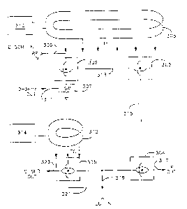
Description of the Pxeferred Embodiment
The preferred embodiment of the invention is a
preselector circuit for a spectrum analyæer. Figure 3
shows a schematic diagram of a tracking preselector
usiny four YIG sphere resonators, 302, 303, 304 and 305.
All four YIG resonators are tuned by a magnetic field
HT, yenerated by field coils 308, which are energized by
control circuit 310. YIG resonator 305, which acts as a
discriminator, is also within a second
l ~'7~
1¦ offsetting magnetic field, H~, generated by smaller fietd coils
21 312, which are energized by control circuit 314.
3¦ Two of the YIG resonators, 302 and 303, have two
4 orthogonal half loops around the YIG sphere, an input loop and
an output loop. The other two YIG resonators, 304 and 305, have
6 one half loop for input and one full loop for output mounted
7 orthogonally around the YIG sphere. In the absence of a
magnetic field, there is negligible electromagnetic coupling
9 between the input and output loops of the YIG resonators.
11 However, with a magnetic field present, signals can be coupled
from the input loop to the output loop through the YIG sphere.
12 Only those signals at or near the resonance frequency,
13 determined by the strength of the magnetic field HT, will be
14 coupled to the output loop, so the YIG resonator works well as
a tunable bandpass filter.
16 YIG resonator 302 acts in combination with switch 307 to
17 switch the input RF signals on coaxial line 309 onto low
18 frequency output line 311 or into the YIG filter mixer network
19 on line 313. Switch 307 is turned off for input signals below
~ about 3 GHz,and the signals are directed to output line 311.
21 Switch 307 is turned on for input signals above about 3 GHz, so
222 the output side of the half loop in resonator 302 is yrounded,
3 and the input signals are coupled through the YIG sphere to
line 313.
YIG resonator 302 is also the first stage of a three stage
26~ passband lter, comprising the three YIG resonators 302, 303
";. :
l ~ 7~35~
1~ and 304. The center frequency o~ the passband filter is tuned
2~ by sweeping the magnetic field HT to track the sweeping Lo
3¦ frequency. YIG resonator 303 is the second stage of the
41 filter, tuned to the same frequency as YIG resonator 302 by the
¦ field HT.
6 YIG resonator 304 has a dual function, as the third stage
of the filter and also as a fundamental mixer, combining the
8 filtered RF input signal on line 315 with the L0 signal on line
9 319 to yield the IF output signal on line 317.
Finally, YIG resonator 305 functions as a discriminator,
11 sensing any difference between the LO frequency and the
12 resonance frequency of the YIG sphere tuned by the magnetic
13 field. The LO signal transmitted through the full loop from
14 line 319 is compared with the L0 signal from line 321 coupled
through the YIG sphere to the full loop to provide an error
16 siqnal output via line 323 for the magnetic coil control
17 circuit 310. A supplemental magnetic coil 312 over YIG
18 resonator 305 provides the offset magnetic field ~0, so that
19 the tuning field HT is actually offset from the L0 frequency by
~ the IF frequency, and the three stage YIG filter is tuned to
22 the RF frequency.
23 The four YIG resonators in combination perform the
multiple functions required for the preselector. By tuning
22~ the magnetic field, the passband center frequency of the filter
26 tracks the LO frequency. The offset magnetic field, Ho/ over
~b ~ tne dl iminator determines the offset of the passband center
7`~
1 equency with respect to the LO frequency. The accuracy of
2 thP offset is dynamically checked and adjusted by the
3 discriminator, peaking the filter without creating any spurious
4 magnetic fields. The mixer YIG resonator 304 combines the RF
and LO signals to produce the IF output signal.
6 In addition, the switch and filter circuits included in
7 the preselector of the invention perform different functions as
8 their frequency dependent impedance changes over the broad
9 frequency range of the spectrum analyzer, to separate the low
and high frequency input bands and to isolate the RF, LO and IF
11 signal paths.
12
13 Switch Operation
14 The input signal for a spectrum analyzer can range from DC
to 22 GHz or higher. To handle this wide range, the input
16 signal is divided into a low frequency band, e.g., from DC to 3
GHz, and a high frequency band, e.g., from 2.7 GHz to 22 GHz.
18 The low frequency band is coupled directly to the spectrum
19 analyzer circuits. The high frequency band must be
21 downconverted before it is applied to the spectrum analyzer
22 circuits.
The high frequency and low frequency bands are separated
23 at YIG resonator 302, by the operation of a pin diode switch
24 circuit 307. Figure 4A shows a more detailed schematic diagram
226 f the PIN diode switch circuit 307 A coaxial input line 309
28 is c eoted to one side of half-loop 331. The other side of
~l~7~
¦ ~ al f -loop 3~1, node 347, is connected by a micros1:rip
2 ¦ transmission line 329 to coaxial output line 311, through an RF
3 ¦ matching network 333 to ground, and through switch circuit 307
4 ¦ to ground. In analyzing the circuit's behavior for high
51 frequency signals, the physical connections to the pin diode
61 switch must be treated as transmission lines, and the frequency
71 dependent impedance of any signal path must be taken into
8 consideration.
9 For low frequency spectrum analysis, the RF input signal
must be directed to coaxial output line 311, which feeds the
11 low frequency signal processing section of the spectrum
12 analyzer. To do this, the pin diode 346 is biased off, so it
13 presents a high impedance path. The capacitor in matching
14 network 333 also presents a high impedance path to ground for
the low frequency signals. In addition, capacitor 348 in
16 matching network 333 in combination with the inductance of
18 output line 329 and half-loop 331 produces a low pass filter,
so the low ~requency signals pass through half-loop 331 and out
19 through the output coaxial line 311 with minimal losses.
2 Voltage source 350, connected through resistors 343 and
22 345 to pin diode 346, provides DC bias for pin diode 346.
Capacitor 340 blocks any DC bias voltage from appearing at node
23 347. Capacitor 340 physically separates PIN diode 346 from
24 node 347, and thus allows the PIN diode 346 to be biased off
without introducing the bias voltage onto the input line ~1 or
2~ 10
I
21~ output line 311. Thus switch circuit 307 operates effectively
l at frequencies down to DC.
3 For high frequency spectrum analysis, the RF input signal
4 must be coupled through the YIG sphere onto line 313. To
S maximize the coupling through the YIG sphere, it is important
76 to have a good RF ground at the output side of half-loop 331.
To accomplish this, pin diode 3~6 is biased on, so it presents
8 a low impedance path to ground. As the frequency increases,
the impedance of the transmission line to the pin diode
increases. Above about 10 GHz,~the RF matching network 333
11 provides t~e low impedance path from node 347 to ground.
3 The equiv~lent circuits for half-loop 331, RF matching
1 network 333 and PIN diode switch circuit 307 are shown in
14 Figures 4B and 4C. In analyzing the behavior of circuit 307
for high frequencies, the physical connections between circuit
176 elements must be treated as transmission lines.
1 When the pin diode is biased off, the equivalent circuit
18 is as shown in Figure 4B, with the pin diode providing
capacitance 346C, about 0.06 pf. Capacitor 340 has a value of
21 8-10 pf, and blocks the DC bias from reaching node 347.
22 Inductance 331L is the equivalent inductance of half-loop 331;
3 inductances 339L and 341L are the equivalent inductances of the
224 connections from half-loop 331 to capacitor 340 and from
capacitor 340 to pin ~iode 346; and inductance 311L is the
6 equivalent inductance of microstrip line 329. The PIN diode
2 off capacitance 346C, in combination with capacitor 340 and the
2~1
l ~.~70~
2 transmission line inductances 333L and 341L, produce a very
high impedance at node 347 for frequencies up to 3 GHz.
3 When the pin diode is biased on, the equivalent circuit is
4 as shown in Figure 4C, with the pin diode providing a
resistance 346R, about 2 ohms. In order to maximize the amount
6 of energy coupled to the YIG sphere, the total impedance from
half-loop 331 to ground must be minimized. However, when the
8 frequency of the RF input signal increases above approximately
9 16 GHz, the impedance at node 347 produced by the path through
the PIN diode 346 to ground increases markedly. Therefore, in
11 order to minimize the impedance at node 347 for higher
2 frequencies, matching network 333 provides a low impedance path
1 to ground for RF signals at frequencies above 10 GHz.
4 Resistor 345, about 10 ohms, provides additional switching
efficiency in the 3-10 GHz range. This resistor will "de-Q"
16 any parallel resonance between the load connected to the output
18 line 311 and capacitor 340 when the RF input signal is grounded
through the pin diode 3~6. Similarly, in the range above 10
19 G~z, resistor 348 will "de-Q" any parallel resonance between
21 the load connected to the output line 311 and RF matching
22 network 333 when the RF input signal is grounded through
network 333.
23
224 Mixer Ol~erat~n
RF signals in the range of 2.7 GHz to 22 GHz which are
within pemsbsnd selected by the tuning magnetic field HT
7~
1 ¦ are coupled through YIG resonator 302. The signals pass to the
2 ¦ second stage filter, YIG resonator 303, on line 313, then to
3 ¦ the ~hird stage filter and mixer, YIG resonator 304, on line
4 ¦ 315. Using three filter stages improves the selectivity of the
51 filter.
61 YIG resonator 304 and its associated circuitry function to
7 mix the filtered RF signals which appear on line 315 with the
8 local oscillator (L0) signals on line 319. Figure 5 is a more
9 detailed schematic circuit diagram of resonator 304.
YIG resonator 304 operates as the third stage RF filter
11 and as a mixer, downconverting the RF signal by combining the
2 RF input signal with the LO signal to produce a lower frequency
13 IF output signal. This downconversion is accomplished using
14 well known diode mixing techniques. Resonator 304 comprises a
YIG sphsre with a full loop 381 and a half loop 383. The input
16 of the half loop 383 is connected to line 315 which carries the
17 filtered RF signal. The input of full loop 381 is connected to
18 line 319 which carries the LO signal. Two diodes, 385 and 387
19 are connected in series across the output side of full loop
~ 381, and output line 317 is connected to the junction point
21 between the diodes. A matching network 391 is connected to
22 line 317 near the junction point between the diodes.
23 The RF signal is coupled through the YIG sphere to full
24 loop 381 that carries the LO signal. The combined signals are
225 applied to series diode pair 385 and 387 to produce the IF
27 signal a co~xi al output line 317.
~ ,,
.
705~3~
1 The L~ signal is applied to the f~11 loop 381 via input
2 line 319. Inductor 390 appears as a high impedance to the high
3 frequency LO signal. The LO signal is split between the upper
4 and lower portions of the full loop 381, and alternately biases
diode 385 or 387 into a conducting state. Matching network 391
6 provides a low impedance path to ground for the L0 signal, so
7 that the LO signal produces a high conductance state in diodes
8 385 and 387 to insure good mixer operation. Resistor 393,
9¦ about 10 ohms, acts with capacitor 394, about 1 pP, to "de-Q"
10¦ any parallel resonance between the IF circuits connected to
21 line 317 and capacitor 392 over the L0 frequency range, to keep
l the impedance at node 395 low. The low impedance path to
13 ground through network 391 also minimizes the leakage of the LO
14 signal over the output line 317. To minimize parasitîc
inductance, and thus minimize the impedance at node 395,
16 network 391 is integrated with diodes 38S and 387 on a
18 microwave monolithic integrated circuit.
The filtered RF signal applied to the half loop 383 is
19 coupled through the YIG sphere to the full loop 381, inducing a
balanced circular current in loop 381. The L0 input point on
22 loop 381 is a virtual RF ground, because the current is
23 balanced, so there is no tendency for the RF signal to pass
down the LO input line 319. At the opposite side of loop 381,
24 the LO signal will gate the RF signal alternately through the
26 two diodes 385 and 3~7, and the IF output line 317 will receive
2B l n et RF current. 14
\
~L~70~
~he tw~ diodes 185 and 387 produce the IF signal current
which is coupled to the IF load of the spectrum analyzer over a
3 coaxial output line attached to line 317. The return current
4 path for the IF signal is provided through the shield of the
coaxial line to the ground plane of resonator 304, then through
6 inductor 390. Although the network 391 is a ground path for
the LO signal, to the lower frequency IF signal network 391
8 appears as a high impedance. Thus the IF signal flows out the
coaxial output line 317 to the spectrum analyzer with minimum
loss.
2 Discrimin_tor Operation
YIG resonator 305 operates as a discriminator, producing
13 an error signal when the resonator is not tuned to the LO
14 frequency. This i5 done by splitting the LO signal, coupling
one portion of the LO signal through the YIG resonator, and
16 recombining the coupled signal with the second portion of the
split signal to produce an output. Because the magnitude and
18 more importantly the phase shift of the portion of the LO
19 signal coupled through the resonator varies from 90 degrees if
the LO signal is not at the resonance frequency, the magnitude
222 and phase difference between the split LO signals will vary if
the LO signal is not at the tuned resonance frequency of
23 resonator 305. The resulting output is the characteristic
24 output curve of a phase discriminator. This output is used as
an error feedback signal to the drive circuit for the magnetic
26 tuning coil of the device.
27
2~ 1S
7~8~
Figure 6 is a more detailed schematic circuit diagram of
resonator 305. Resonatcr 305 includes a full loop 361 and a
4 half loop 363. The LO signal is split by a divider network
S comprised of resistors 373, 374, 375 and 376 and applied to the
6 full loop 361 via line 319 and to the half loop 363 via line
7 321. Two diodes, 365 and 367 are connected in series across
8 the output side of full loop 361, and output line 323 is
9 connected between the diodes. Also connected to the junction
point between the diodes is a matching network 371.
The LO signal covers a multi-octave bandwidth, and the
11 discriminator must also operate over a multi-octave bandwidth,
132 with the two portions of the LO signal arriving in phase at the
14 full loop 361 and at the half loop 363. To achieve this, it is
important to make the resistor divider network physically
small, with the values and physical placement of the resistors
176 precisely controlled.
lB The portion of the LO signal applied to the full loop 361
19 over line 319 produces current I incident on diodes 365 and
367. The other portion of the LO signal, coupled from half loop
2 363 through the YIG sphere to full loop 361 if the LO frequency
22 is at or near the resonance frequency, induces circulating
23 current i incident on diodes 36S and 367. Thus diode 367
24 receives current IT1, the phasor sum of currents I and i, to
produce a positive voltage VT1 at node 368. And diode 365
26 receives current IT2, the phasor sum of currents I and -i, to
27 produce a negative voltage VT2 at node 368. The discriminator
28 16
~7~35`~
1 tput v~ltage VOuT is the algebraic sum of voltages VTl and
3 Matching network 371 provides a low impedance path to
4 ground for the LO signal, so that the LO signal produces a high
conductance state in diodes 365 and 367 to insure good mixer
67 operation. Resistor 397, about lO ohms, acts with capacitor
398, about 1 pf, to "de-Q" any parallel resonance between the
8 circuits connected to line 323 and capacitor 396 over the Lo
9¦ frequency range, to keep the impedance at node 368 low. The
lO ¦ low impedance path to ground through network 371 also minimizes
21 the leakage of the LO signal over the output line 323. To
13~ minimize parasitic inductance, and thus minimize the impedance
at node 368, network 371 is integrated with diodes 365 and 367
14 on a microwave monolithic integrated circuit.
The operation of resonator 305 as a discriminator is
6 illustrated by the phasor diagrams of Figures 7A, 7B and 7C.
Figure 7A shows the phasor relationships when the LO is at the
18 resonance frequency of the YIG resonator 305. At resonance I
19 and i are exactly 90 degrees out of phase, so that ITl and IT2,
21 and therefore VT1 and VT2, are equal in magnitude. Thus VOuT
22 is zero. Figure 7B shows the phasor relationships when the LO
is below the resonance frequency of the YIG resonator 305.
23 Below resonance +i i5 less than 90 degrees ahead of I and -i is
24 more than 90 degrees behind I, so that ITl is greater in
magnitude than IT2. Thus VTl is greater than VT2 and VOuT i5
26 positive. Figure 7C shows the phasor relationships when the LO
27
2a ~ 17
~7~;8~
l¦ i above ~he resonance frequency of the YIG resonator 305.
2¦ Above resonance +i is more than 90 degrees ahead of I and -i is
31 less than 90 degrees behind I, so that ITl is smaller in
41 magnitude than IT2. Thus VTl is smaller than vT2 and V0uT is
negative.
6 Figure 8 shows a plot of V0uT verses ths frequency of the
7 LO signal, with the origin set at the resonance frequency of
8 the YIG resonator 305. It can be seen from Figure 8 that,
9 between points 403 and 405, V0uT varies directly as the
difference between the LO frequency and the resonance frequency
ll to which YIG resonator 305 is tuned. Thus V0uT is positive
12 below point 401 where the tuned YIG resonance frequency is
13 above the LO frequency, V0uT is zero at point 401 where the LO
l~ frequency equals the tuned YIG resonance frequency, and V0uT is
negative above point 401 where the tuned YIG resonance
16 frequency is below the LO frequency.
7 Because of this relationship, the discriminator output
18 vOuT is used as a feedback signal to control circuit 310 to set
l9 the magnetic field HT on the YIG resonators, thereby varying
22o their resonant frequency to accurately track the LO frequency.
22l The discriminator of the invention is not limited to the
tracking filter-mixer application of the preferred embodiment.
23 It can also be applied to a variety of YIG tuned structures,
24 for example, a tracking filter with single or multiple stage
YIG tuned resonators without a mixer stage.
26
27
22