Note: Descriptions are shown in the official language in which they were submitted.
~70~6~
Optical sensor
The present invention relates to an optical sensor com-
prising an optical waveguide, and, more particularly, an
elastically deformable optical waveguide.
Conventional optical sensors, whether electrical or
mechanical, have various drawbacks. For example, the elec-
trical sensor suffers from electromagnetic interference and
is not essentially explosion-proof. The mechanical sensor
not only has a complicated structure but also suffers from
deterioration of its moving parts.
One object of the present invention is to provide a
sensor that avoids the drawbacks of the conventional sensors.
Another object of the present invention is to provide a
novel optical sensor that utilizes the elastic deformation
of an elastomeric material.
To these ends, the invention consists of an optical
sensor comprising an optical waveguide having an optical wave-
guide member of a transparent elastomer surrounded by cladding
and through which light can be propagated, wherein the amount
of propagated light can be changed by elastic deformation of
the waveguide member.
" ,, ~.
_ ~,
'f~6~
-- 2
In the drawings:
Figs. lA and ls illustrate the principle of a sensor
according to the present invention,
Fig. 2 is a cross sectional view of one embodiment of
a press button,
Figs. 3A to 3D are perspective views of sensor elements
according to the present invention,
Fig. 4 is a cross sectional view of another embodiment
of a press button,
Figs. 5A and 5B are schematic cross sectional views in
different positions of a pressure sensitive sensor utilizing
flexural deformation,
Fig. 6 is a perspective view of a liner switch,
Fig. 7 is a perspective view of one embodiment of a
membrane switch,
Fig. 8 is a cross sectional view of another embodiment
of a membrane switch,
Figs. 9 and 10 are graphs showing relationships between
light transmission loss and the applied load.
The op~ical waveguide member of a sensor according to
the present invention is elastically deformed by the appli-
cation of an external load, whereby the amount of light propa-
gated therethrough is changed. This load may be applied to
a part of the waveguide or to the whole waveguide. When the
load is removed, the waveguide returns elastically to its
original shape, so that it can be repeatedly used.
Preferably, the waveguide member is made of a trans-
parent elastomer. Specific examples of a suitable trans-
parent elastomer are polysiloxane elastomer (silicone rubber),
polyurethane rubber and polybutadiene rubber. Among these,
polysiloxane elastomer is preferred, since it has better trans-
parency. A rigid material such as silica glass, multi-com-
ponent glass, ceramic or a rigid plastic (e.g. polymethyl
methacrylate) is not suitable for making the waveguide
member.
. ~
~270~
-- 3
The optical waveguide may be an elongate one, and its
cross section may be round, square, rectangular or any other
shape. The optical waveguide may have a flattened cross
section.
The waveguide usually has cladding that reflects the
light propagated along the waveguide member, such cladding
surrounding at least a part of, and preferably all of, the
periphery of the waveguide member. This cladding can be re-
placed by any means that will reflect light and prevent leak-
age of the propagated light.
The cladding should have sufficient mechanical strength
that the optical waveguide can be repeatedly elastically de-
formed without the cladding being destroyed. Preferably, the
cladding serves as protective means for the sensor. In the
case of an optical fiber comprising a core and cladding, the
core serves as the waveguide member.
The cladding is made of any material that can reflect
the light propagated along the waveguide mernber. Specific
examples of suitable cladding material are fluororubbers,
silicone rubbers, fluororesins (e.g. tetrafluoroethylene/
hexafluoropropylene copolymer, polytetrafluoroethylene and
the like), polyurethane rubbers, polybutadiene rubbers, and
so on.
The cladding is usually made of an elastomer having a
smaller refractive index than that of the waveguide member
(e.g. fluorine-containing elastomer), although other material
such as plastics can be used. The cladding material is pre-
ferably transparent.
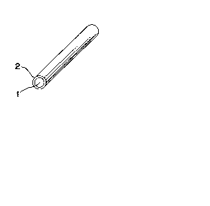
Figs. lA and lB illustrate the principle of a sensor
according to the present invention. In these figures, the
optical waveguide is an optical fiber and the elastic defor-
mation is a compression deformation. The sensor comprises
a waveguide member 1 with cladding 2 surrounding the member 1.
Light is propagated from one end of the fiber to another.
When a load is applied to a part of the sensor in a direction
~7()~
- 4 -
shown by an arrow F, the sensor is flattened, as shown in Fig.
lB, so that the amount of light transmitted is decreased in
comparison with the unflattened state of Fig. lA. The amount
of transmitted light is changed if the load is applied to any
S part of the waveguide along its length. The waveguide recovers
its original shape of Fig. lA after ~he load F is removed and
can therefore be used repeatedly.
Various embodiments of sensor according to the present
invention will be explained, without limitation to the scope
of the present invention. In the following figures, only a
part of each sensor is shown, the optical fibers for the in-
cident light and for the emitted light and spliced parts being
omitted for simplicity.
1. Pressure-sensitive sensor
. _ . .
lS The pressure-sen~itive sensor of this embodiment utilizes
compression deformation, and is illustrated with reference to
a press button.
Fig. 2 is a cross section of the press button which com-
prises a button 10, a casing 11 and a sensor element 12. Figs.
3A to 3D are perspective views of the several sensor elements.
In each of these figures, the light can be propagated from the
front to the rear of the element.
Fig. 3A shows an element comprising a round optical wave-
guide member 13 with rectangular cladding 14; Fig. 3B shows an
element comprising a square optical waveguide member lS with
rectangular cladding 16; the members 13 and 15 extending from
front to rear of the elements. The cladding 14 or 16 has a
smaller refractive index than that of the waveguide member
13 or 15 and may be made of an elastomeric material, and may
serve as a protective layer. The elasticity of the cladding
helps restoration of the press button to its original position.
The waveguide member may be of a shape other than round or
square.
Fig. 3C shows a sensor element comprising an optical wave-
guide member 17, cladding 18 and a protective layer 19 sur-
rounding the cladding. The cladding may be a tube made of an
-- 5
elastomer or a plastic, the waveguide member and the cladding
forming an optical fiber.
Fig. 3D shows a sensor element comprising an optical
waveguide member 20 in the form of a sheet sandwiched ~etween
sheet-like cladding 21 which may be plastic film. This sensor
element can also have an elastomeric cushioning layer on at
least one of the cladding layers.
Fig. 4 shows a press button 22, the sensor element 23
shown in Fig. 3D and a housing 24, an upper portion of the ele-
ment 23 being engaged by a downward protrusion from the button23.
2. Pressure sensitive sensor
A pressure sensitive sensor utilizing flexural deformation
is shown in Figs. 5A and 5B which illustrate the sensor before
and during the application of a load. This sensor comprises
a button 30, a sensor element 31 and a support 32. The sensor
element 31 may be any of those shown in Figs. 3A to 3D, light
being propagated from one end of the element 31 to the other.
3. Strain gauge
This gauge measures change of the amount of light propa-
gated through an optical waveguide due to a change of the
cross sectional area and the length of such waveguide caused
mainly by a tensile load (not shown).
4. Load-sensing transducer
The sensor elements of Figs. 3A to 3D can be used as part
of a load-sensing transducer (not shown).
5. Linear switch
Fig. 6 is a perspective view of a linear switch, which
comprises an optical waveguide member 40, cladding 41 and
covering sheets 42. The optical waveguide member is made of
an elastomer, the cladding is made of an elastomer or a plastic,
and the covering sheets are made of plastic. The upper and
lower covering sheets may be heat sealed together. When a
load is applied to at least a part of this device along its
length, the amount of transmitted light is changed. If such
a linear switch is attached to one end of a sliding door, it
can detect material trapped between the door and its frame.
6. Membrane switch
Fig. 7 shows a membrane switch that comprises optical
waveguide members 50, a panel 51 and a base plate 52. The
panel 51 is an elastomer sheet and the base plate is a
plastic or elastomer sheet. On the inner surfaces of the
panel 51 and the base plate 52 there are several grooves
53 in which the waveguides are embedded. On the upper sur-
face of the panel 51 there are indicating marks 54 formed,
for example, by printing.
Fig. 8 is a cross sectional view of another embodiment
of membra~e switch which comprises a matrix member 55 and
optical waveguide members 56, the member 55 acting as clad-
ding.
Since a sensor according to the present invention util-
izes light as a medium to be changed by the external load,
it is not affected by electric and/or magnetic fields. It
functions elastically and has good durability, as well as
a simple structure. A very thin membrane switch can be
produced, and, by adjusting the elasticity of the elastomer,
it is possible to vary the sensitivity.
Practical and presently preferred embodiments of sensors
according to the present invention are explained by the
following examples.
Example 1
An elongate cylindrical sensor comprising an optical
waveguide member made of polysiloxane elastomer having a
diameter of 2 mm and cladding made of tetrafluoroethylene/
hexafluoropropylene copolymer having an outer diameter of
3 mm was fabricated. Over a length of 50 mm of this sensor,
a load was applied and the light transmission loss was
measured. The relationship between the applied load and
the light transmission loss is shown in Fig. 9. When the
load was repeatedly applied and removed, substantially
the same results were obtained. Fig. 9 shows a good cor-
relation between the load and the light transmission loss.
~-~7~
7 --
Example 2
An elongate cylindrical sensor comprising an optical
waveguide member made of polysiloxane elastomer having a
diameter of 1.8 mm and cladding made of a fluororubber
having an outer diameter of 2 mm was fabricated. Over a
length of 10 mm of the sensor, a load was applied and the
light transmission loss was measured. The relationship be-
tween the applied load and the light transmission loss is
shown in Fig. 10 which shows a good correlation between the
load and the light transmission loss. When the load was
repeatedly applied and removed, substantially the same
results were obtained.