Note: Descriptions are shown in the official language in which they were submitted.
~2~
A BIPOLAR INVERSION CHANNEL DEVICE
Back~round of the Invention
1. Field of the Invention
The present invention relates to a device
structure suitable for transistors, thyristors, optical
emitters, optical detectors, and other solid state
devices.
2. Description of the Prior Art
The speed of operation and transconductance
are two properties of transistors that device designers
ll) are endlessly seeking to increase in order to obtain
suparior performance. The present invention is directed
to a novel device that combines aspects and virtues of
known bipolar and MOS devices and, among other
advantages, has high current gain and high
1~ transconductance coupled with relatively simple
~abrication requirements and low charge storage.
Summary of the Invention
We have invented a solid state device wherein
an inversion layer controls the flow of electrical
7~ carriers between two regions. The device is desiynated
in one illustrative e~mbodiment, the Bipolar Inversion
Channel Metallic Emitter Transistor (BICMET), and
comprises a metallic emitter in ohmic contact to a
wider bandgap region; a narrower bandgap collector
region; and a channel contact which contacts an
inversion layer formed at the interface between the
wider bandgap region and the narrower bandgap region.
Other regions can be added to obtain other devices,
including thyristors, optical emitters, etc. The
principle of operation is based on controlling the flow
of majority carriers from the emitter to the collector
by the biasing action of charge in the inversion layer,
which can provide for current gain. A conversion of
~C~ photons to hole-electron pairs can be obtained,
3 ~ producing an optical detector.
- , : -
.- ,. .. . . ~
., ' :'~ ' ' ~'' ';' . ' .
:~L~7~33
- la -
In accordance with an aspect of the invention
there is provided a solid state device comprising an
interface between first and second regions having a first
conductivity type, and adapted to the formation of an
inversion layer at said interface, with said inversion
layer being in electrical contact with a source of
electrical carriers of a second conductivity type and
adapted to control electrical carriers of said first
conductivity type flowing between said first and second
regions.
~.
.: : , :
:
-- 2 --
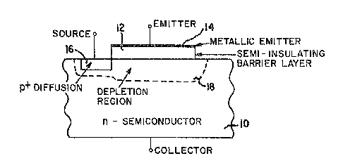
FIG. 1 shows a cross-section of one embodiment of
the BICMET; the regions are not to scale, with the barrier
layer (wider bandgap region) being shown thick for
illustrative purposes.
FIG. 2 shows the zero bias (i.e., equilibrium)
energy diagram of a p-channel BICMET.
FIG. 3 shows the BICMET in the off state.
FIGS. 4 and 5 show the internal current flow
patterns in the BICMET.
FIG. 6 shows the terminal current flowing in a
BICMET circuit.
FIGS. 7 and 8 show an energy diagram and hole
concentration with distance for the semiconductor depletion
region under forward bias.
FIGS. 9 and 10 show a heterojunction, and BICMET,
formed with InGaAsO
FIG. 11 shows a n-channel AlGaAs - GaAs BICMET
energy diagram.
20FIGS. 12-15 show process se~uences for an
A1GaAs - GaAs BICMET.
FIG. 16 shows a p-channel SIPOS-Si BICMET energy
diagram.
FIGS. 17-20 show process sequences for a p-channel
SIPOS-Si BICMET.
FIGS. 21-25 show device characteristics for
p-channel SIPOS-Si BISMETS.
FIG. 26 shows device characteristics for a
n-channel A1GaAs - GaAs BICMET.
30FIG. 27 shows device characteristics for an
AlGaAs - GaAs BICMET, with a graded collector energy gap.
FIG. 28 shows the effect of collector stretching
on a p-channel Si BICMET.
FIGS. 29-30 show device characteristics for the
p-channel Si BICMET with and without collector
~.
,.. . :.,
,, ;~,,"; , .: ~
3~7~3~
stretching.
FIG. 31 shows a diode connected BICMET and
characteristic.
FIG. 32 shows a BICMET photodetector cross-section
(in Si).
FIG. 33 shows the equivalent circuit for the
photodetector connected to an amplifier.
FIG. 34 shows a BICMET optical emitter.
FIG. 35 shows electrical characteristics of a
BICMFT optical emitter and thyristor.
FIGS, 36-38 show energy band diagrams for the
structure of FIG. 340
FIG, 39 shows a BICMET thyristor.
Phy~ical Structure
An illustrative physical structure of the BICMET
is shown in FIG. 1. The following discussion considers a
"p-channel" device, wherein a p-type inversion layer is
formed at the interface between n-type materials. An "n-
channel" device is analogous, with the conductivity types
~0 being reversed. However, the terms "minority carriers" and
"majority carriers" are generic to both device types.
Electrons are designated the majority carriers, and ho1es
the minority carriers, in the p-channel device, since the
bulk of the material is n-type. For consistency, this
designation is maintained in the inversion layer as well,
even though it has p-type conductivityO These designations
are of,course reversed for the n-channel devices. This
designation scheme implies that the minority carriers are
of a different conductivity type than the majority çarriers
in a given device. The term "bandgap" refers to the
difference in energy levels between the valence band and
the conduction band for the material of a given region of
the device.
The p-channel BICMET comprises (FIG. 1) an n-type
relatively narrower bandgap materiaI, which is designated
.~ :
: , i . . . .. . ...
- : -::: . : :: : : . .
~7~!~33
-- 4 --
the "collector". In one configuration, referred to as
"emitter up", the collector is formed in a supporting
substrate 10, which may be a semiconductor wafer or an
epitaxial layer formed thereon. Contacting a surface of
the narrower bandgap region is an n-type relatively wider
bandgap region 12 (designate~ hy "semi-insulating barrier
layer") which is suf~iciently thin to permit thermionic
carrier transport throu~h the film, but sufficiently thic~
to prevent tunneling. A metallic layer 14, referred to as
the "emitter", contacts this region, with the wide bandgap
region 12 separating the metallic emitter 14 from the
collector 10. A metallic emitter is used because a semi-
conductor is not really a very efficient emitter; it is, in
fact, a limited source of carriers and, invariably, its
resistance becomes a dominant factor at high current levels.
On the other hand, a metal, with its almost infinite supply
of carriers, its low resistance, and its inability to store
charge, has all the basic features of the ideal emitter.
The problem, of course, is to achieve a structure that will
incorporate a metal to ~ake advantage of these features.
In the present structure, the metallic layer also serves to
create or enhance an inversion layer thereunder, by means
of the field effect between the metallic layer and the
collector. By aligning the edge of the metal layer to a
~5 "source", discussed below, this field effect thus creates
or enhances electrical access to the inversion layer, for
contr ,o3 purposes. As discussed below, the metal layer may
be formed in electrically isolated segments, with a
peripheral portion serving to control access to the
inversion layer, and another portion serving as the
emitter. These portions may be overlapped slightly and
isolated-by a dielectric to ensure a continuous inversion
layer.
In the p~channel BI~MET, a p+- well 16, adjacent
to the metallic emitter, provides electrical access to an
,~
~: , :";: . - ,
,. , ; ..
, .
~7~3!3~
inversion layer 18, also referred to as the "inversion
channel" herein. This access well is designated the
"channel contact" herein; it is alternatively referred to
as the "source. This is because the channel contac~ serves
as the source of minority carriers that control the flow of
majority carriers across the inversion layer. An
"inversion layer" can also be referred to as a "two-
dimensional gas", although not all two-dimensional gases
exhibit inversion. The p-channel BICMET thus has a two-
dimensional hole gas, and the n-channel BICMET has a two-
dimensional electron gas, in the inversion layer. Note
that the term 'lelectrical con~act" as used with regard to
the source implies that the inversion layer is supplied
with minority carriers that flow directly from the source,
and thereby control the flow of majority carriers from
emitter to collector. This implies that the control
carriers (in the inversion layer) are of opposite
conductivity type to the controlled carriers (flowing from
emitter to collector). This is in contrast, for example,
~0 to an enhancement mode field effect transistor operating in
the common gate configuration. In that case, the
controlled carriers flowing from source to drain are
identical with the control carriers flowing from the source
(into the inversion channel), and hence both control and
controlled carriers are of the same conductivity type. As
used herein, the term "operating electrical potential"
refer,s,to the application of a voltage between the emitter
and collector that tends to cause majority carriers to ~low
from emitter to collector. The absence of any exte~nally
applied electrical potentials to the source, emitter, and
collector is referred to as the 'Iquiescent'' state herein,
and the device is also referred to then as being in
"equilibrium".
EnergY Band Diayram
The energy band requirements of the BIC~ET under
'' ~'' , ~ ,' :
~7~3~
equilibrium conditions are illustrated in the energy
diagram of FIG. ~. In the interests of clarity, we herein
also refer to the wider bandgap (thin-film barrier layer
14) material as a "semi-insulator" and the narrow bandgap
material 10 as a "semiconductor", al~hough neither may
necessarily fall within the accepted definition of these
materials - e.g., they could both be semiconductors or
semi-insulators. Furthermore, these terms do not imply
resistivity differences, since either may have a larger
resistivity than the other, or they may have comparable
resistivities. In addition, the terms "narrower bandgap"
and "wider bandgap" are defined for material in the
vicinity of the inversion layer. This is because the
bandgaps can be graded in either region away from the
inversion layer, as by a change in crystal composition or
doping levels, as explained further below. For purposes of
analysis, the semiconductor material is assumed to be
sufficiently thick that it accommodates the depletion layer
formed at its surface under operating bias. On the other
hand, the semi-insulator is assumed to be sufficiently thin
that: (a) the electric fields within it are essentially
constant; (b) that electrons and holes pass through without
substantial scattering - that is, conduction processes are
thermionic; and (c) recombination and space charge effects
are negligible. Typical thicknesses of the semi-insulator
range from 70 angstroms to 1 oon angstroms, and more
typica,lly 150 to 400 angstroms.
The symbols utilized herein are defined in the
Table, below. Note that * as a superscript demotesian
~ :
~ .. .~ .
- . : . . ~ : ..
- , : : ., ,:,. .:,
, ,, ~
- ~: - : , : -
Sl~mons-~aylor 1-2 ~ 3
equili~rium value.
- ,;5 IS~ - QF - ~r~LLs
~ device area.
A Richar~son~s co~stant (=120
amF cm /degreeK ).
Ci capacitance of the semi-insulatin~ layer.
d thickness of the semi-insulating layer.
, D hcle ~electrcn) diffusion constant
P n in tha n-type tP-tYpe) semiconductor region~
10 EFn Fermi level in n-ty~e ~emicbnductor bulk.
~E~n energy difference bet~een Fermi level and
conduction bend in n-type semiconductor.
E , E , E i' E conduction (valence) band energies in the
C V C Vl ~emiconductor and in the semi-in~ulator,
respectiYely-
Eg, E~i ~and g2p energies of the semiconductor and
semi-insulator, respectively.
Ei equilibrium el~ctric field in the semi-
insulator (~-Vi/d).
~ 6s semiconductor dielectric corstant.
G dc current galn of the BIC~ET.
Ic, IE, Is ccllec~or, emittert source currents,
respectively.
J , I hcle current flo~ com~onen~ from source
25 pc pc to collector ~density and total curren~
resFectively)O
J i~ I i hole current density and total hole
F ~ current in the 5emi-insuIator.
J , I qeneration current density and clrrent
30 9 D (respectively) in the collector -
depletio~n region.
J , I electron current density and to~al
ni nl eIectrical current in the semi-
lnsulator.
3~ JE emitter current density.
JC collecto- ~rrent density~
. ~.
Simmcns-Ta~lcr 1-2
3~
~ 8
L hole diffusion leDgth ln the
P n-tY~e semiconduc~or.
~e effective ~ass of an electron.
Nc dencity of states in the conduction
band of the semi-ins~lator, or
semiconductor (assumed the same for
convenience)~
N density of states in the valence band
v cf the semi-~nsulator, or the
semiconductor (assumed the same
for convenience).
~d~ Nd~ donor concentration in the semi-
conduc~or and semioins~lator,
respectivelyO
15 ni semiconductor intrinsic carrier
concentrat~on.
~s voltage bandobending of the
semiconductor de~letion region.
2¢~ ice the equilibrium Fermi ener Qy
in the bulk semicon~uctor.
= -qV + ~ electron barrier hei~ht at the
c i n semi~on~uctor sani-insulator interface.
m211 barrier ~or electrons at
n the metal semi~insulator interface.
.
25 ~ energy barrler for holes at ~he semi-
P ccnduc*or semi-irsul~tor interface,
~E , ~E conduction (valence) band ed~e
c v discontinuity bet~een semiconductor and
~emi-insulating b~rrier; see FIGo
30 ~ '' equilibrium surface potential
S of the semiconductor-
change in surface ~otential of
the se~lconductor under bias.
-qY =~ -~ voltage drop in the semi-insulator
3~ i c n ~ith zero b~as a~plied.
p surf3ce co~^entration of
holes (cm 3~
~ulk concentration o~ holes in
no the n-~y~a~se~cQnductQr.
: "; : ,
. ~i :: : :::
- ~ , ~.::~ , . .
: : ~ ~ . ,. .: . :
Simmcns-Taylcr 1~2
33
_ 9 _
P ~guilibrium concentration of holes
at the semiconductor surface.
p(x ~ hcle carrier concentration at
d the edge of the depletion regionO
5 Q charge Per unit area in the semiconductor
s ~ith bias applied.
Q charge per unit area in the semiconductor
~ith no bias a~Flied.
~ electronic charge.
10 ~ , Q immo~ile charge ~er uni~ area, and
i i squilibrium immobilQ cha~e ~er unlt area,
at the semlconductor ihter~ace.
Q , Q~ ~cbile charge per unit area 2ni
lnv lnV equil1brium mobile charge per unit area
in the semiccnductor.
~d depletion char~e per unit a ea in the
semiconductor.
Qst total stored char~e per unit area (=Qs~Qs)
in the BICMEI un~er bias.
~0 Q ~ stored~o~ile charge per unit area
st~ t=~-Q~ in the BIC~ET under
R~e common emitter output r esist an ce .
sg generation lifetime of the semiccnductorO
25 V saturation veloci~y (taken to be - 10
s cm/sec for Si-SIPOS in~e~face or the
tbe AlGaAs-Ga~s interface).
Vt ,v,th thermal velocity of holes,
P lectrons (res~ectively),
in the semi-insulator~
V , Y ~olta~e and equillbriam ~oltage across
the s~mi-insulatin~ bar~ier layer,.
Yi ~i Vi
Vsc cource-~ollector voltage.
35 Y~E source-emitter voltage.
V E ccllector-e~tter voltage.
C
Xd colle~t~r de~letion width.
::
:
,- :. : ~
,.: . :: :
:: ~ " .:, , .. ::- : :
. .
Simmorls-Taylor 1-2
~275~33
-- 10
1~ q/k~
k Eol~zmann 's constant .
T absolute temperature~
energy of acceptor leYel above valence
5 ~ kand.
~E., ~F position and equilibrium position
ar.d equilibrium ~osition Fermi læ~el slith
respect to the valence band.
The ~os. s~riking feature of the BICNET i~
that the -ollector depletion r~gion extends
substantiallY to the semi-insulator inter~ace, typically
e~an ~ithout bias; i.e., even in the quiescent state.
The energy level of the conduction band of the
se~iconductor is c~n~inuously increasing as the surface
is a~roachea, and there is an inverted laYer at the
surface. As used herein, the term "inversion" refers to
a field-induced layer at the sur.ace of the
semiconductor that interfaces ~ith the semi-insulator,
~h~ch layer is of op~osite conductiYity type to that of
the bul~ ~f the semicondu_tor. In a typlcal embodi~ent,
the absolute ~alue of the surface potential ~5 ) is
~reater than twice the Fermi level (2~) of the
semiconductor bulk with no bias ~oltages applied,
resultin~ in an ener~Y ~and configuration similar tc an
ideal ~OS depletion transistor. The formation of the
in~ersicn layer is ty~ically accomFlished in part by
charge deposition ~e.g., ion implantation~ molecular
beam eFitaXy, or ot~er im~uritY do~ing methods~. The
depth of deposi~ed charqe from the lnterface is
ty~ically less than 100 angstroms for the de~osited~
charge ~ensity cf 1C19 carriers/cm3- Ho~e~er~ greater
depths are ~ossible,!as long as the ~depositlon region
remainC electricallY dePleted o~ char~e carriers. It
can also be accomplishea at least in part by choosing
~he ~ide and narro~ bandgap materials to haVe
sufficiently di~fer~nt ~ork ~u~ctions, that 19~
different ~ermi lev~Is, so that invercion occurs. ~The
.., ~ - ,
: ' ~ ' ~ ' ;.,; ' ;, ' ',. '`` .
:. ' ' :"~`' '
., .~ ..
Si~ons-TaYlor 1-2
33
- 1 1 =
~terials shoYn herein ha~ve ~F~roxi~ately comparable
Fer~i levels, so that the use o charge depos~tion is
~escribe~ belo~) Hc~ever~ ~he inversion can ~lso be
acco~lishea ~otally or in ~art ~y short channel effects
or o~erating bias, discussed further belov. T~e
discon~inuity bet~e~n the valence ~ands, or bet~een the
conduction ~a~ds, due to the difference iD ~he bandgaps
of the ~aterial on either side cf the ~nversion laYer,
~rovides for confine~en~ of the 1nYersion char~e. For
10 this ~ur~ose, the diffe~ence in the ~alence band
aner~ies ~Ev) for the p-channel BICMET, or in the
con~uction ban~ ener~ies ~Ec) ~or the n-channel BICMET,
is at least 0.025 electron volts. ~or example, we
estimate that a difference of 0.0~ electron volts
provides for retainlng about 87 percent of the inversion
charge in the inversion layer.
Therefore, the aICMET is significantly
different from the hetero~uncticn transistor, ~hich is
simply a b~polar ~unction transistor ~ith the base-
emitter ~-n ~UnctiOD re~laced by a heterojunction ti.e.,
a ~unctlon bet~eeD tw~ semiconauctors havin~ different
bandgaF energie~)O Consequently the hetero~unction
transistor typically has the ~ro~lems associated with
the bi~olar ~unction transistor and, in addition, a
sa~ere ~roblem ~ith recombination at the heterojunction
lnterface due to una~oidable lattice ~ismatches. The
BIChET, on the other h~nd, has no base as such, being
&o~r'ised of two contactin~ layers of the same type
~e.~., n-type), ~s op~ose~ to three semiconductor layers
ln bl~olar ~unction transistors an~ heteroiunction j
bi~olar ~unctlon translstors. ~hile the inversion layer
of the ~IC~ET ~Day be ~ormea by counter-aoping of a
semicon~uctor ~e.~, for~ing a ~-layer in an n-
naterial), Dote that ~he base of a conYentlonal bipolar
35 transistor $~ formed to have a ~uiescent carrier density
DUC~l ~re~t~ tb~s~ th~ cll~r~ in~ctod by the o~eratin~
bias. For examFl~ t11e carr~er ~en3ity in tS~e ~s~e o~ a
.
.,, ,, .., ~,.. . . .
, '' ' ;' '"' '
~ - , '
SimmQns-Taylor 1-2
3~
_ 12 _
bipolar transistor is ty~ically about 1017 to 101~
carriers~cm3, ~ith ~he injected charge densitY during
operation being typically an order of magnitude less.
In contrast, in the BICYET, the density of carriers in
the inversion laYer during operation is typically at
least 1~ times, and frequently over 1~0 times, as great
as the quiescent carrier density due to the deposited
charge. For example, the inversion layer sxtends less
than 100 angstroms, and typically less than 50
angstroms, from the semiconductor - semi'insulator
in~erace. Hence, an exemplary carrier density of holes
~pO) of 1018 carriers/cm3 produces a sheet charge
density of only abo~t 3x10 carriers/cm in an
exemplary ~0 angstrom thi-k inversion layer. ~his is
substantially less then the density of charge (holes in
the case of the p-channel aICMET) injected from the
source into the inversion laYer during o~eration.
Furtharmore, the operating bias potentials increase the
level of inversion, which inherently produces a charge
density greater than the b4ckground charge.
The resulting quiescent inversion channel is
thus supplied with holes from the channel contact when
the device is biased. The condition of inversion
substanti411y reduces recombination and trapping of
charge in interface states. A reduction of
recombination and trappin~ can also be accomplished by
ot~er techniques (e.g., hydrogen annealin~ ln the case
o the' Si/~IPOS interface), which may reduce the amount
o~ inversion necessarY for this pur~ose~ The
e~uilibrium field Ei in the semi-insulator is positi~e;
i.e., the e~uilibrium semi-insulator volta~e is
negative, Vi ~ O. As noted above, the inverslon channel
is formed so as to exist at least in ~art with no bias
voltages applied. Ihis can be accompli~hed by
depositing charges at the interf2ce, ei~her in the
semiconductor or semi-insulator, or both. TypicallY~
sufficient charge is de~osited so that the Fermi level
..
Simmons-Taylor 1-2
12 ~33
13
in the inversion layer is within 0.2 electron volts of
the v~lence band for the p-channel BICMET, or ~ithin 0.2
electron vclts cf the conduction band for the n-channel
BICMET; most typically those values are ~ithin the range
o$ 0,05 to 0.1 electron volts.
The inver~ion can alsc be accomPlished totally
or in part by the short channel effect. This can be
induced by making the source-collector junction dee~er
relative to the channel length, or by making the channel
relatively shorter. Then, the dePletion regions due to
the source-collector ~n ~unc~ion can exte~d
substantially tc the limits of the interface between the
semi-insulator and the semiconductor. The electric
fields at the depletion region edge can then cause
inversion even in the absence of deposlted charge at the
interface cr operating electrical potentials. In fact,
~t channel len~ths on the order of 0.1 micrometer, it is
expected that no additional doping (i.e., charge
daposition) at the interface is required to achieve
~0 inversicn. ~s noted above, the operating electrical
potentials also act to increase the inversion charge,
and it is possible to achieve inversion totally by the`
biasing voltage applied to tbe de~ice. However, this
typically results in an increased turn-on voltage (VcE,
cut-in) that is undesirable in many cases, but may be
acceptable or desirable in other cases.
In order to realize the full potential of the
BICMET, the channel contact should provide good
electrical contact to the inversion layer. This is
advantageously obtained by sel~-alignment of the channel
contact to the emitter. Tlen, the p diffusion of the
channel contact electricallY accesses the inversion
layer at the semi-insulator - semiconductor interface;
see FIG. 1. It is possible for the metallic emitter to
overlap the channel contact to some exten~, in order to
ensure good electrical access. This can be
accomplished, for exam~le, by heating ~he channel
''~ '' ~ ' : '
Simmons TaYlor 1-2
~l~t~33
1 'I --
contact region to cause the (P) dopant to diffuse under
the edge o~ the semi-insulating region. Ho~ever,
increasing the overlap causes i~creased parasitic input
c~acitance of the device. It is also possible to space
the channel contact a short distance from the ed~e of
the semi-insulator; ve astimate that distances up to the
depletion ~idth associated with the source-collector
juncticn, and Perha~s even beyond, may be accePtable
before increased resistance effectively eliminates
electrical access of the inversion layer from the
channel contact. This depletion width is typicallY on
the order of 1000 angstroms. Any barrier between the
c~annel contact and the inversion layer should typically
be onlY a diffucion ~arrier, and not a ~ield de~endent
conductivity region. However, it is possible ~o utilize
a field-deFendent ccnductivitY region for control
purposes. That is, the metal layer can be divided into
two (or more) regionC, an~ an additional control
electrode (not shown) can contact the region between the
source and the emitter contact, as vie~ed in FIG. 1.
These metallic re~ions can then be somewhat overlapped
at their edges and dielectrically isolated, thus
isola~ing the control electrode and the emitter
electrode. Then, aF~lication of the aP~ropriate voltage
~5 to this control electrode can create or enhance the
inversicn layer t~ereunder, producing electrical access
from ths sourca to the inversion layer under the
emitt~r. Alternately, the apPli~ation of the opposite
volt~ge to this control electrode can reduce or
ali~inate such accecs to an inversion layer otherwi~e
present. Note also that while FIG. 1 sho~s a single
c~annel contact, additional contacts can be provided
around the periphery of the semi-insulator. In fact, a
continuous annular channel~contact aroun~ the semi-
insulator can be prov1ded, for imProved access to theinversion layer.
; " ~ ', ,. :
,
~, .
Simmons~Taylor 1~ >7~33
_ 15 -
In a typical embodiment, the emitter of the
BICMET is formed on a different level than the channel
contact, see FIG. 1. This allows the channel contact to
be separated ~rom the me~allic emitter by the semi-
insulator, and hence avoids hi~h source-emitter leakage
currents. Further, this non-Elanar geometry allows the
source to contact the inversion layer in a self-aligned
fashion, as noted a~ove. Note that this geometry is
different than the typical planar geometry of bipolar
transistors, where a p-n iunction isolates the base from
the emitter. In an alternate e~bodiment, referred to as
'emitter down~', the emitter is formed in the s~bstrate~
and the collectcr ic formed on a mesa on the substrate.
An emitter contact spaced a shor~ distance from the mesa `
contacts the emitter, whereas a channel contact on the
substrate contacts the inversion layer, as before, still
other ccnfigurationc are possible.
~ e note that there is a similarity between the
source current in the ~-channel BIC~.ET and the source
tor channPl) current of a p-MO~ transistor, since both
feed the current flc~ing in the p-channel inversion
layer at the semiconductor surface. However, the ~ICMET
does not require a drain, since the source current flows
through the semi-insulator to the emitter. This
proYide~ the aICMET with two distinct advanta~es
~amongst others) vis-a-vis the ~OS transistor, namely:
~a) the phenomenon of NOS punchthrough does not exist,
~hich h~s important scaling im~lications; (b) the device
begins to turn on immediately when channel charse begins
3~ to flow; therefore tha del~y associated with the cha~r~e
transiting the ~OS channel ~rom source to drain is
eliminated (although there is a much shorter delay time
for the electrons to tra~el from the emitter to
collectcr o~ the ~IC~ET, which is a distance ty~ically
of the order of 600 angstroms). Because the BICMET does
not haYe the punchthrough cons~raints of the MOS or
bipolar transistors, it may be scaled to much ~maller
:" ,' ,. :' , ~:
: : ,: : .; . : . . : .
Simmons-Taylor 1-2 ~7~33
dimensions. In fact, there ap~ear to be no obstacles in
scaling the lateral dimensions into the sub 0.1 ~m
range.
As noted above, the formation of the inversion
layer is typically enhanced at cmaller dimensions bY the
~short-channel" effect. Referring ~o FIG. 1, the
depletion reqion, even in the absence of deposited
inversion charge, or an operating electric~l potential
applied to the device, will extend from the source (P
di~fusion) under the semi-insulator. Thi~ is of course
due to the usual formation of a de~letion Fegion at a
p-n junction, as carriers miqrate across the junction
until electrostatic orces establish an equilibrium with
diffusion forces~ At smaller device geometries, the
~5 source (P diffusion) tyFically becomes deePer relative
to the width of the semi-insulatorO ~ence, the
dePleticn region extends further under the semi-
insulator, until at some ~eometry it extends entirely
under the semi insulator; iOe., it extends to the limits
~0 of the semiconductor - semi-insulator interface. Since
the inversion layer is aFproximately co-extensive with
the ~epletion region at the interface, this short-
channel effect can ~y itself ~rc~uce the desired
inversion layer, 0~ course, the inversion is ~ur~her
enhanced when Ferating electrical potentials are
~pplied, as noted above.
~ he function of the semi-insulator is to form
a potebtial barrier to electrons (~n ~ qvi)~ and holes
(~p) at zero voltage, between the emitter and the
collectcrO Ideally, the emitter/semi-insulator con~act
should be as close to ohmic as possible, i.e., ~n should
be less t~.an 0.1 el~ctron volt, and preferably less than
0.05 electron volt. Note then any contact potential
between the metallic emitter and the semi-insulator is
transparent to the external circuit, and hence not
included in ~n. Th~ low "on" r~sistance o~ the device
allo~s a saturated ccllector current densitY (iOe., when
~ . . .
.~ .
,, : : '
' ~ ~'.' -:
. ~ .
Simmons-Taylor 1-2
3~7~3
~ 17 ~
Yi>Yiton)) of at least 106A/CM , and a carrier density
of at l~ast 1013 carriers/cm3 transiting the wider
band~ap region. T~ requirements of these barriers and
the pràctical implementation of the structure will be
5 further discussed below.
E YilibriY__Ch~g~_3~_Volt3qe-~-stEibutions
In all of the ener~y diagrams herein, energy
bands sloping uFwards to the right as viewed imPlY a
neg~tive voltage drop across that region and hence
positive fields, and energy bands t~at slo~e do~nwards
in movinq to the right imply positive voltage change and
negative field. Thereore, for ex~mple in Fig. 2, ¢s is
a positive quanti~y and Vi is negative. The e~uilibrium
charqe relationchiF for the ~IC~ET is
15 Qe + Qc ~ Q; t1)
-
* .. *
where Ce Q5 and ~i are the charge per unit area on the
emitter, in the collector (semiconductor) and at the
se~ insulator - se~iconductor interface. Under
e~uilibriu~ conditions the surface of the semiconductor
~0 is heavilY inverted; thus (see equation ~3b o~ the
appendices)
* t29~5) I * ~ *~1/2
Qs ~ r~ ~ I Po ~d~sa I t2)
*
uhere pO, the e~uilibrium hole density at the interface,
is given by
~5 Po = Nv~e QEi/kT = N e t.g ~EFn-q¢s)/kT
It is worth notin~ that since the eauilibrium field in
the semi-lnsulator is positive, then Qe > O, and since
Q5 > then from t1) Qi = ~ (Qe + Q_) so Qi< for the
energy band configuration shown.
The aquilibriu~ surface potential ~s and
semi-insulator voltage Vi are related as follows:
~ . .
: ::: :
: . ,: : . .,
.~
, .. , .. ,. ,,,~.... .: :
. . :: .. ~ , ,. ": :: ~, , , :
Simmons-Taylcr 1-~
0~3~
- 18 -
Vi ~ ~s = _qS ~4)
~here ~ is the difference in work functions of the
ms
metal (~m) and semiconductor (~s)
(5)
ms m s ~
* ~
Vi and ~5 are relat~d to ~n and ~p by
- ~EF + ~Ec + q~s+ qvi = ~EFn c ms
and
= ~ qV ~ ~E + Egs - q~5 - ~EFn ~Ev ~s Fn ~s
We. also have
Egi ~n p
* *
and Vi is related to Qe by
Vi = Qe/C~
~here Ci is the caFacitance per unit area of the semi-
insulator.
~HE^RY_CF_CPERATION
The p-~hannel BICMET operates as a current
am~ ier by allowing source hol~ current to flow, which
~orces a much greater emitter - collector electron
current to ~low. tThe n-channel BICMET operates by
allowing source electron current to flow, forcing a much
greater e~itter-collector hole current to flow-) Thu~s
the BICNET is a b1~o1a~ device ~hich manifests current
gain and, as such, may be compared to the junc~ion
bipolar transistor. However, there are several
~5 distinguishin~ features of the ~ICKET vis-a-vis ~he
bi~olar transistor. Firstly, ncte that a biPolar
transistor has a neutral b~se; that is, a base region
having no Fotential gradients (i.e., 1at ener~y bands).
The BIC~IE~ does not have a neutral base; that ls, it has
. ~
:.:: , :: . :
: :.::,.. - ..
, : . ~:i: ::: . : :
.. - : ~ ' :,., . ~
Simmcns-Taylcr 1-2
3~
_ 19 --
electric fields on ~oth si~es of the interface. Thus,
all of the problems associa~ed ~ith the conduction of
e~itter-collector current in the base, ~hich includes
minority c2rrier diffusion, carrier scattering, base
charge storage effects, high-level injection and the
phenomena of punchthrough, do not exist, or are at laast
substzntially reduced, in the BICMET. All these base-
related prcblems present serious limitations to the
s~itching speed of a neutral base device. tThe
practical requirements of implementing inversion charge
at the int~r~ace may make it desirable to ~rade-off some
desirable Fropertie~ to some ex~entO Powever, we limit
any neutral region in the vicinity of the interface to
have a thickness of less than 100 angstroms; it is more
typically less than 30 angstroms.) Secondly, the emitter
is metallic, and as a consequer.ce the emitter resistance
is very lou. ~hus it can carry much higher current than
a semiconductor emitter, and the emitter charge storage
is negligible. As used herein! the term "~etallic"
~O applied to the emitter refers to a material ha~ing a
volume resistivity of less then 0.001 oh~-cm at the
device operating temperature. It thus includes true
~etals, ~ich typically have resistivities of less then
100 microhm-cm at 2C degrees C. It can also include
metal compounds (e~g., silicides), and degenerately
doped semiconductor material; i.e., a doped
semicondu_tor whose Fermi level is in the conduction
band ~-ty~e) or in the valence band (~-type).
In the following analysis, the emitter is
assumed to be grounded ~i.e. only the source and th~
collector po~entials vary), so all voltages are with
reference to the emitter pot~ntial. Under normal
conditions of bias ~FIG. 3), the collector and source
are positively biased.
Off-State I = O
~ -- C
FIG. 3 illustrates the device in the off
~tato, that ls, ~ith IS ~ ~ h 0 po~itivo ~oltavo
i", '' ~ '' '
,. . , ... ~ .-: .. : ~,,
: .:: ` . .:
:i, ,: : :: ~
, , . ,: , . .
. :. , ~
Sim~ons-Ta~lor 1-2
~7~33
- 20 -
ap~lied to the collector, the semiconductor goes into
partial deeP deF~etion (~5 > ~s) because of the leaky
nature o~ the semi-insulator. In other words, in the
steady-state conditicn, the holes generated in the
de2letion region of ~he semiconductor are transported
through the semi-in~ulator:
Jpi Jg qXdni/Tg,
~here Jpi is the hole current flowing through the semi-
insulatcr, Jg i9 th~ current generated in the deFletion
re~i~n, xd is the semicon~uctor de~letion region width,
ni is the intrinsic carrier density and Td is the
semiconductor lifetime.
In order fcr the semi-insulator to be caPable
of transporting the generated carriers, it must be
aPproPriatelY biased. This is achieved by the build-uP
of inversion charge within the inversion layer, creating
a voltage drop Vi given bY (see A2)
Vi ~ Yi = (Qs 2s)/Ci (10)
where Vi is the voltage drop across the semi-insulator,
~ Ci is the capacitance oE the semi-insulator, and Q5 ~ Q5
is the change ln th~ semiconductor charge under bias,
where Q is given hy (see A3a)
(2 6_~ IP ~ \sltNd qVS~ (11)
and Jni is the semi-insulator electron current as
discussed shortly.
~ hen the insulator is biased to Vi, the
barrier to hole flo~ from the inversion la~er to the
emitter is lowered ky an amount QYio Consequently,
holes in the inversion layer are iniected into the
semi-insulator, resulting in a net flow of holes throu~h
the ~emi-insulator to the emitter. The flow of hoIes
give rise to a curr6nt densitY Jpi given by (see ~18)
.. ,
.: .. " -:
-, ' ': '',. ;...... .. ... -~ ~ :,. ..
: . .-.,: .:. : : .
-,, : , ., : . . ; :.
:,: - . ~: .,: . : , ,
Simmons-Taylor 1-2
~2~ 33
-Vl+~E /~ av.
Jpi = qvpP~e [ l-13. (12)
Since Vi and hence Qs ~5 and pO are quantities
predetermined bY th~ fabricatio~ procedure, then
e~uations (1-5) permit the determination of pO and Vi-
Similarly, biasing the semi-insulator reduces
the barrier to electron flow frcm-the emitter to the
collector, resulting in a net electron flow of (see .a.18)
~ q( ~Vl ~
Jni = qYnNce c ~e -1~. ~ (13)
On leaving the semi-insulator, the electrons are
iniected into the collector and join the generated
electrcns to produce the collector current. Generally
speaking, since conceptually ~he device is designed to
produce current gain~ Jni Jpi ni g
Consequently, the ccllector current is essen~ially equal
to Jni
Jc ~ Jni~ (14)
~here ~e have assumed that the reverse flow is
negligible. It alsc follows from the principle of
current continuity that
Je ni pi' (15)
w~ere Je is the current density entering the emitter
contact.
The_BICNET_as an_A~Plifier,_Ic_>_Q
In this s~ction ~e will consider the
characteristics that allow the ~IC~ET to produce current
gain. Also, W9 will conslder only the dc
characteristics; th~ dynamic characteristi.cs are
considered elsewhere. Generally speakinu, the source
current that flows into the inversion channel will be
30 considerably larqer than the very smaLl current
:
: ,...: , . ~ ., ~. -
,, .- ., . ~ , .
Simmons-Taylor 1-2
~Z~3~
- 22 -
generated in th~ collector depletion region, so the
latter may be ignored from now on. Since IC is
considerably greater than Ig, pO and thus ~Vi must
increase to provide the necessary biasing condition to
support the flow of the source current through the
se~ insulator. Biasing the semi-insulator also causes
electrons to flow from the emitter thro~gh the semi-
insulatcr into the collector, where the high field
swee~s the electrons into the neut~al section of the
collector tFIGS. 4-~). If the semi-insulator is thin
enough, the c~-riers ~ill enter the collec~or
t~armionically. Provided the doPln~ is high enough so
that~the depletion width is thin enough and the
depletion field is high enough, the carriers will be
"hot" throughout the collector region; i.e. the carriers
move with the saturated drift vslocity. ~ith a suitable
choice of materials and geometries, it can also be
designed to operate totally or ~artially ballisticallY-
This is facilitated by the use.of a relatively thin
depleticn region znd thin collector, providing for a
high field and reduced carrier collisions with the
semiconductor lattice, and hence a high current density.
There is no limit on how thin the semi-insulator may be
made ~rcvidad the ccntact is ohmic, or on the width o~
the dapletion region, other than dictated by capacitance
considerations cr tc avoid tunneling. Another Point to
note is that the emitter can supply a much greater
elect~dn current to the ~emi-insulator than the
inversion channel can supply hole current to the semi-
insulatcr, because cf the much lower barrier hei~htlatthe emitter. Thus, the structure contains the basic
reguirements for c~rrent ~ain.
I. Volta~e Equati_ns
The voltage Vi droP~ed across the se~i-
insulator is still obtained through equations (10), (A2)
and tA3). The oth~r relev~n~ Yo~t4~s ~ as ~ollow~-
The source-emltter voltage is ~ven by tsee ea~ation A4)
:: :
"
.
Simmons-Taylor 1-2
33
_ 23 -
-1 *
~SE d~i +~ ln(pO/pO). (16)
It is interesting to note that the insulator voltage is
not egu~l to the source-emitter terminal Yoltaqe- This
~s a consequence of the spli~ting o~ the quasi-Fermi
levels at the semi-insulator/semiconduc~or in~erface
~see ~ppendix A.1). he source-collector voltage is
given ky ~see equation (A5))
V = ~Yi + ~ 11n(pOJPO) ~ VCE = fl ln(Po/Po s
and the sur~ace potential of the collector is giYen by
(see Al)
~s VcE - Yi + ~5- (18)
and ~s = ~s ~s
II. CuEren_ ~u~t}ons (~Vi < ~c)
The terminal currents for the BICr.ET are shown
in Fi~ 6 and the various intern21 currents are shown in
FIGS. 4 a~d 5, from which we have
IE = Ipi + Ini~ (19)
IS IFi Ipc' (20)
I = I - I . (21)
~0 It is implicitly assumed in (13) that recombination in
~nter~ace states or in the semi-insulator does no~ n~eed
to be considered. Ihis assumption is justified in the
appendices.
Follo~inq (12) we have for the hole current in
~V .
the semi-insulator, assuming e l 1 as normally ~ill
be the case,
~qQY.+qVi-~E )/kT
pi = qAvp~Oe 1 v (22)
" ~ . .. ' ' .
" ' ~
Si~mons-Taylor 1-2
- 24 ~
and for the electron current in the se~i-insulator from
(13),
tq~V ~ kT
Ini = QAvnNce l c (23)
The current component Ips is the por~ion of
the source hole current that flows out of the collector;
it ~as significance only at low VcE, ~hen ~s ~ ~s~ To
understand the origin of this current, we refer to Figs.
4, 5~ 7, and 8. As Eo builds uF to bias the semi-
insulator, the Fer~i level EF~o at the semi-
insulator/semiconductor interface moves clpser to thetop of the valence ~and:
~ = N e Fpo v (24)
At suffi-iently lo~ VcE when EFn > EFpO, the
semiconductor surface is f~rward-biased to the holes.
~e may, therefore, look at the semiconductor de~letion
region as an induced one-sided p -n ~unction with Po
representing the hole carrier density in the p section.
Thus, we have for t~e hole carrier concentration p(Xd)
at the edge of the depletion region
p(xd) = pOe s (25)
Assuming that the neutral section is several diffusion
lengt~s long, and u~ing the long diode equation to
calculate the resulting diffusion current, JPC, we have
qD ~D ( ~ ~
Jpc- l_E (F(Xd)-Pno~= L- I~Oe ~Pnol' (26)
where Pno (=ni/Nd) is the e~uili~rium hole density in
the neutral n-secticn. As~YcE and hence ~5 increase,
eYentuallY EFp~ > EFn~ In effect, the induced P -n;
~unction is now re~ersed-biased, 50 I~c ceases to flow,
and all the source current is now ~orced to flow through
~ " . '. ' , ~ '
. .~ '. ' '' ,
,, . , ' ' '''' ;'' '
Simmcns-Taylcr 1-2
~7 l;P~33
- 25 -
the semi-insulator. The reverse-biased induced junction
will now be a source o~ qenerated holes which will flow
towards the semiconductor surface; however, as
previously noted, ~his current is negligible com~ared
~it~ the source current and will not be considered
~urther.
III. Current 5ain
Small-signal current gain is defined 25
dICJdIs ~ith Ipc = I Thus, frcm (20-23) we find,
assuming vp = vn,
~ IC N (dE -~ )/kT
G = ~ e . (27)
dIs po
Normally, we would require ~n~' so wi~h a suitable
choice of ~Ev the gain can be very large. For example,
~or ~Ev = 0.3V and po~Nc, which is typical a~ w~ discuss
in the next section on silicon technology, current gains
of over 104, and ty~ically on the order 105, are
attainable. Gener~lly spe~king, current gain ~ill
decrease with increasing source current and, hence,
increasin~ collector current. The reason for this is
that a larger pO and avi are required in order to
sup~ort a larger sauree current - see (22) - and, from
(27), G is inversely proportional to pO. It is also
noted that the gain incre~ses rapidly with decreasing
temperature; however, the emitter and hence collector
currents for a given QVi decrease rapidly with
tem~erature. These ~end to be cancelling effects,
although IC doec ~ncrease for a constant IS as the
temperature is reduced.
DEVICE_S~UCTVR_S
III=V_~t~r~l_Teçhnologiec
The use of high mobility materials has long
~eer. proposed as a superior alternative to Si ~or high
speed ICs. Ho~ever~ the advantages have been difficult
to reali2e because c~ ~he problams in ~brica~ing viable
bipolar or MOSFET d~vicesO The only device available
, ~ ,
:; ; ~ .. . ..
.. ",.' ,,~ ~ ~
'. ,'''.,` I` "" " ' ''
, ,. '' , ' '
'' ''." ' , ,
., ,, ~,,
.. , , ~
Simmons-Taylor 1-2
33
.
- 26
for GaAs integrated circui~s, for example, is the MESFET
(~etal Emitter Shottky Field Ef~ect Transistor) ~hich
suffers from the Problems of threshold control and logic
swing for enhancement-mode technolo~ies. Additional
problems are excessive power dissipation and
requirements of leY~l shifting for depletion-mode
technologies. The EICMET offers a means of implementing
a hiqh-performance device structure in nonsilicon
materials. The structure appears particularly
attractive for thos~ material combinations which have
already bean demonstrated using Molecular ~eam E~itaxy
t~BE) techniques; cee for example, U~ S.
Patent 3,615,931, "Technigue For Growth of EPitaxial
Com~ound Semiconductor Films", coassi~ned with the
present inventionO
The contrcl and uniformity obtained in sim~le
heterostructures are more than adeguate for fabricating
the BICMET structur~. For exam~le, n-InP/n- -
InO 53GaO 47As heterostructures have been fabricated
having ~ood electrical characteristics. A ty~ical
energy diagram for this combination is shown in FIG. 9
~here the InP is restricted in thickness to about 300 A.
~e also note that the band-gap discontinuities of
~Ec = 0.21 eV and LEV = 0.4 eV are particularly
~ttractive to form a p-channel BICMET with very hi~h
current gain. ~ow thi~ structure does not have the
desired e~argy band configuration shown in FIG. 2
because the narrower-bandgaF semiconductor is
accumulated rather than inverted. However, cor.sider; the
structure sho~n in FIG. 10. Here the wide-band-~ap
layer of InP is doped very close to the surface using
MBE techniques with acceptor ions over a distance of
abont lC-30 angs~rom with a concentration of NA = 119
cm 3. The concentration of this charge m~st be
sufficiently lar~e to cause inversion of the interface.
(It is possible to achieve the same result by doping the
narrow-band-gap semiconductor in a similar fashionO
:
~ ,,, ' . ,, :
-. . . ~
. ;. ...
.: -:: :
-:- : ,, .,: . :,
,:,, .- ' , . . .
Simmons-Taylor 1-2
3~
~ 27 -
However, since it i~ desired to avoid the formation of a
neutral base layer, it is desirable to locate the
acceptcr on the wid~-~and-gap side of the interface.)
Tha InF layer is to be doped n-type to approximately
Nd = 1019-1018 cm 3 with a suitable dopant and the
thickness is chosen to be less than the equilibri~m
depletion width corresponding to the doping of the InP
so that ~he entire layer is dePletedO For doping
concentrations in the range 1Q18 cm 3, the TnP thickness
~ould therefore be about 200-300 angstroms. It will be
noted that the doPing level in the In~ is considered
sufficiently high and hence the ener~y barrier
represented by the dotted line sufficiently thin that it
is totally transparent to electrons, as one always finds
at an N~Si/metal contact. It ~ight appear at first
glance that the transparent barrier at the emitter
interface constitu~es a sPecific contact resistance in
the same fashion that a metal does in contactin~ a
juncticn. However, in this c~se there is no neutral
section in the contact re~ion, so that part of the
source em1tter voltage tVcE) is actually droPPed across
the transparent barrier. There~ore, the interfaci~l
resistance will be lower than that encountered in a
conventional ohmic ccnt ct of the SaDe do~ins.
The AlGaAs-GaAs system is a very attractive
candidate because of the technology base that ~as
already been established in the development of the ~H
(double heterojunction) laser. For this case the
relevant energy parameters are ~Eg = 0.4 eV, aEC = 0.32
and QEv = 0.08. To realize maximu~ gain, the chann~l
carrier is chosen that provides the maximum barrier to
semi-insulator conduction. Therefore, an n-channel
BIChET is chosen, ~ith electron conduction in the
inversicn channel. The energY diaqram for this
transistor is shown in FIG. 11. In principle, for the
n-channel BICNET, ~v is ideally zero. The converse is
true tor the ~-chann~l ~ICM~T; l-e-, ~Ec ~ ~ In both
: : .' ~ ,::: ::
. ' : : ::
.
Sim~ons-Taylor 1-2
- ~.2~ 33
cases, it is decira~le that ~g is maximized~
In FIGS. 12-15 we show a cross-section of the
transistor, indicating how it can be fabricated in an
integrated circuit ~echnology. The starting material is
semi-insulating gallium arsenide upon ~hich successive
layers are grovn usin~ molecular bea~ epitaxy. The
layers in sequence are: (i) GaPs (p-type, 1017-1018
c~ 2 ~m); (ii) GaAs (n-type 10 9 cm 3, 10-
30 angs~roms); (iii~ AlGaAs (p-type 101~ cm , 300
400 angstroms)~ The concen~ration at the top surface of
the AlGaAs is increased as high as possible to assist in
ma~in~ the best possible ohmic contact. A refractorY
metal such as tungst~n and an overlayer of CVD (Chemical
Vapor Deposition) oxide are deposited and patterned and
then the oxide is used as an etch mask to rem~ve the
AlGaAs material as shown in FIG. 13. Then more CVD
oxide ic deposited and reactive ion etched to protect
the AlGaAs sidewall. Using either one or two resist
masking steps, implantation is used to create an N
self-aligned source contact and a p collector contact.
~The ~+ contact does nct need tc be self-aligned). The
device can no~ be annealed at 800-830 degreeC without
danger cf interacticn between the tungsten and AlGaAs or
of significant im~urity ion motion. Finally, the
contacts are metallized with the use of an additional
layer of dielectric isolation. Alternately, the
dielectric isolaticn could be put down earlier in the
sequen~e to allow emitter metal to cross the mesa edges.
Another ~rnary combination which is
attractive for the BIC~ET and which is presently
receiving much attention becauce of itC application to
the 1.3 ~m fiber optic need is InAlAs - InGaAs. In this
case ~Ec = 0-3 eV and ~Ev = 0.2 eV so the n-channel
BICMET is still the Freferred choice. Other
possibilities are the combinations ~lAs-GaAs and
A10 5InO 5P_GaO 6IDO 4hs, both cf which are known tc
have a reasona~le match in l~ttice constants (hence
.,. ~ ; ... ..... ,. :
::: : . : .
;. ,.,, , :.. :.. .
:,., , ::
:. . , :: : .;, ., ::
: . :, :
. ,.:. ., :. .
,
~:,. . .:
. .
Simmons~aylor 1-2
- ~7~3~3
-29
controllable interface state densities) and attractive
c and ~Ev values. Another possibility is the choice
.71 .29 ,63P.37~Inp ~i~h the discontinuities
~Ec = 0.22 eV and ~Ev = 0.18 eY. Clearly, the possible
combinations of materials are ~ide, and the choice will
be presumably dictated by the application, ease of
~abrication, etc,
Furthermore, we estimate tha~ lattice mismatch
will hava a relatiY~ly small effect on device oFeration~
because the zero-bias inversion condition inhibits
recombination throuçh anY states that do exist. As a
result, many material combinations (for the semi-
insulatcr and semiccnductor) that are poorly matched maY
also be considered. Not only are a wider range of group
III-V ccm~inaticns Eossible, but also groUPs II-YI
_ombina~ions. The atomic spacing of different
semiconductor materials ty~ically m~st be within 3
percent of each other for hetecojunction transis~ors.
In contrast, the BICNET can o~erate satisfactorilY with
~reater mismatches. ~e estimate that it can o~erate
satisfactorily even for materials differing greater than
5 percent in atomic spacin~. rhis also imPlies that
either the seml-insula~ing region, or the semi-
conducting region (or both) can be polycrystalline or
amorPhous. (Note in ~act that SIPOS is typiczlly
amorphous.) Hence, the low rate of recombination at the
inverted inter~ace allows device structures (e.~.,
vertica'l stackin~ and materials not previously viable
in some cases.
Silicon Technolo~
_____________ _
The BICMEI structure in silicon technology can
be implemented by using a deposited SIPOS fllm on a
silicon su~strate. For SIPCS deposition techniques, see
for example~ "Semi-lnsulating Polysilicon tSIPOS)
Deposition in a ~o~ Pressure CV~ Reactor, I, Growth
Kinetics", M. L. Hitchman et al, Jo~rnal of Crystal
Growth, Vol. 55, ~o. 3, p~. ~85~500 ~also see pp. 501-
.:: , :
. . .
'' ~. ., ,, ~ ,
,. . .
Simmons-Taylor 1-2 ~ 3
_ 30 _
509) (1981)l It hac been sho~n with suitable
fabrication procedures that SIPOS may be Produced with a
band qa~ of about 1.5 eV, and resistiYities in the range
108 _ 101 ohm cm. ~owever, SIPCS do~ed with ~hosphorous
or boron, followed by high-temPerature annealing, has
resistivities in ~he range 10 1 to 10fiohm-cm. The
high-temperature annealing aP~arently activates the
dopants, causin~ the Fermi level to move from ~idsap to
the appropriate band edge. SIPCS has, in fact, been
used to produce high-gain heterojunction transistors.
Phosphorous-doped SIPOS appears to produce a barrier,
c = ECi ~ EC at the SIP~-Si interface of about
.2 eY and a barrier aEV Ev EVi of about 0.3 0.4 eV~
The energy diagram for this BIC~ET configuration is
shown in FIG. 16. Pgain a surface layer of acceptor
ions is re~uired at the interface between the SIPOS and
the Si to create an inversion Iayer. In this case, it
~ould not typically be feasib~e to ~lace the ~
interfacial adjustment ch~r~e layer in the SIP~S by MBE.
Thus, in this case it would be desirable to deposit the
l~yer at the silicon surface by MBE. This layer should
be suf~iciently thin (10-30 A) to avoid the possibilitY
for a ~neutral) base layer to exist. Ps noted above, if
the length of the c~annel is m~da small enough, two-
dimensional charge-sharing effects can automatically
c~use inversion of the interace. This "short-channel"
phenomenon is ~ell known as a detrimental efiect in
sub-m~ron MOS devices. In order to induce this effect,
the channel length is typically less than about three
times the de~th of the depletion region of the channiel
p well. If the source junction were located on both
sides of the emitter, then the maximum channel length is
about slx depletion depths.
Proper ccnstruction and doping of the SIPCS
film is of si~nificance for obtaining optimum device
performance. It is ~ro~osed to use MRE (molecular beam
epitaxy) or extremely low energy implants ~ollowed by
.
;: , ~
. ::. : .,,
., ~,
,:: .: :: ::
,
:: - ,,
,. .:.. . . . .
Simmons-Taylor 1-2
31
ra~id thermal annealing ~o achieve the hishly localized
charge layers. A silicide (Ta, W, or Ti) is a good
choice of metal for the emitter because (a) it allows
the impl~ntation of a self-aligned channel-emitter
junction to feed the inversion channel (b) it tolerates
the suhsequent high temperature annealing re~uired to
activata the imPlant. It is likely that RTA (rapid
thermal annealing) can be advanta~eously used to produce
the highly localized charge pro~iles. A typical ~rccess
~equence is shown at the im~ortant steps in FIGS~ 17-20.
Side~all oxide ~rotection during the imPlantation steF
as sho~n prevants the doping of the SIPOS sidewalls.
DEVICE_CHARACTERISTlCS
Based on reason~ble parameters, the various
device characteristics have been generated for the
structuxes described above,
SIpQS=S~_Systems
In order to discuss the device characteristics
and to relate them to the Physics in a simple and
~0 straightforward manner, ~e will initially ignore space
charge e~fects in the collector due to high collector
current densities. These space~charge effects result in
Partial neutralization of the donor density in the
semiconductor (i.e., creates a neutral region) which
causes an increase (stretchinq) in the semiconductor
depletion re~ion ~idth. This e~fect we designate
"collector stxetching". At the end of this section we
~ill include this effect in a ~ractical design to assess
the limitations it im~oses. PhYsically speaking, the
~0 in~ection of mobile electronic char~e into the colleçtor
depleticn region ca~ses a debiasin~ o~ the barrier layer
(i.e., less net ~ositive -harge available to bias the
barrier layer) and h~nce a reduction of the emitter-
collector current flow. Furthermore, the ~pace-char~e
modul~tion of the ccllector cuxrent, coupled with the
transit time delay cf the carriers through the collector
de~ lon ro~lon, o~ona th~ po~ y o~ ~ tun~bl~
-
: , -
: . ,:
-.- . ,
: ~ ..~.
,:
Simmons-Taylor 1-2
_ 32
low-noise solid-state oscillator ca~able of frequencies
in the infra-red r~sion (ap~roaching the f~ of the
transistor - 1600 GHz); i.e., a coherent source,
FIGS. 21-23 illustrate the common-emitter
output characteristics of the SIPOS-Si BICNET shown in
the inset of FIG. 21. All three curves have identical
material p ~ ameters except for the silicon dopin~
concentration which varies as ~ = 1015, 1017 and 1018
cm ' for FIGS. 21-23 respectively. In the calculations,
the relative dielectric constant for SIPOS was taXen as
8, vtn = vtp = 107 cm/sec and the t~.ermionic conduction
limit was assumed. The ~ICMET common~emit~er output
characteristics of EIGS, 21-23, are similar in structure
to bipolar common-emitter output ch ~acteristics, with
lS t~o obvious differences. The first of these is the very
hi~h gain of the ~IC~ET, typically 2x10⁴, which is of
the order of 200 times greater than for bipolar
transistorsO The second is the high collector current,
typically of the orde~ 1O6 A/cm2, yielding a maximum
2~ transconductance of approximately 4x10⁷ A/(cm2 - V~,
~hich is almost an crder of maqnitude greater than that
of the bipolar transistor. On tbe debit side the
VcE ~ut in is some~hat higher at (0.2V) than found in
bipolar transistors, but this is not considered to be of
any serious consequence. For the non-silicon materials
the use of M~E allo~s us to grade the bandgap of the
collactor ~rom narrow b~nd gap at th~ interface to wide
band g,a~ at the de~letion edse. This technigue can
reduce the VcE~ cut-in to almost 2 ero as shown below.
The collector current is observed to be
negatiye at low Vc~ (<YcE~cut-in)
consequence of the fact tha~ the depletion region of the
semiconductor is for~ard-biased, thus providing a low-
lmpedance path for the holes from the channel to the
collector. To supFcrt this~flo~ of holes, pO needs only
to be small, because of the relatively low semiconductor
barrier hei~ht ~s tsee tl9)). Because ~O and hence Qs
., .,; .::
" ~, :
, ,, .. .. ~
':. : ~ . .,, :
Sim~ons Taylor 1~2 ~7~33
_ 33 -
are small, ~Vi is very sm~ll so Ini is much 1QSS than
Ipc, resulting in n~gative collector current (see (21)).
As VcE and, hence, ~s increases, ~0 and, thus~ Qi' must
increase to maintain constant base current. HoHever,
increacing pO results in an increase in ~Vi and~
consequently, in I~i an1 Ini. Cut-in occurs when
Ini = Ip5; that is, when Ic = (see (14)). For typical
parameter Yalues fcr the SIPOS-Si system, VcE for this
conditicn yieldS VCE,cut-in 0-2 3 hi
transition to the ~ider bandgap material (i.e., grading)
can thus reduce VcE, cut-in, lt is also possible to
achieve this result by an abruPt transition. That is,
an additional laYer cf material (not shown) can be added
to the bottom of the collector region shown in FIG. 1.
This additional layer can have a bandgap larger than
that of the collector material in the vicinity of the
interface. The narro~er bandgaF collector material can
then have a thickness of perhaps one, or a few,
depleticn widthc.
Further ~ncrease in VcE, and thus ~s~ causes
~0 and hence ~Vi and Ini 9 ~- IC) to increase further
still. Eventually Ini, and hence Ic, saturate when
essentially all the channel current flo~s through the
semi-insulator, i.e., Ipi ~ Is. At this point, pO and
~5 ~V~, and hence Ini, become constant, so the collector
current becomes conctant. Further increase in VcE
simply causes ~5 to increase (since ~Vi is essentially
consta~t - see (21). Provided that the change in the
~h~rge in the depletion region due to increasing ~s is
small ccmPared to ~0, then the semiconductor charge i
Qs = Qi ~ Qd~ and thus Vi, ~ill remain essentially
constant, since (see Appendix A1) V~ 5~Ci. With Vi
constant Ini, and hence Ic, remain essentially constantO
This happens to be the situation for the output
characterictics of the BICMET skown in FIG. 21, which
has a semiconductor doFing concentration of 1015 cm 3,
as is apparent by the very ~lat satura~ed section o~ the
"
,
. ~"' ' :'' ,:
.,~
Simmons-Taylcr 1 2 ~ 9
34
curves. The dotted curve in FIG. 21 illustrates the
stored charqe Qst = Qs Qs for s
predicted, it is seen that Qs- Q5 incre7ases wi2th VcE and
finally saturates at a value of 2.7x10 C/cm ~hen the
output curves saturate; i.e., when VcE = VcE sat. The
inYerse of the cloFe of this saturated portion is the
common emitter output resistance Ro~ which is derived
elsewhererefl61 Roe = ~I-N . Thus, for a device
delivering 10 mA and usin~ the typical value of
10 PQ = to19 cm 3 R = --- 1-2---15 = 2x10⁴ ohms, which is
typical of a bipolar transistor delivering the same
current.
In contract to the flat saturated section of
the output characteristic of FIG. 21 it is seen that the
saturated sections cf the out~ut characteristics in
FIGS. 22 and 23 increasa m~rkedly with increasing VcE.
The reason for this is the high semiconductor dopin~
(1017 and 1018 cm 3) of the BICMET which causes the
charge Qd in the deFletion region to make a substantial
contribution to the semiconductor charge Qs- Thus, as
~5 increases beyond its value at saturation, Qs
increases due to the increase in Qd' Qs = Qi + Qd' which
causes Vi to increase beyond its saturation value.
Conse~uently, Ini a~d, hence, Ic increase with
increa~ng VcE, the effect being more pronounced the
greater Nd, as is apparent from a comparison of FIGS. 22
and 23. The saturation section of the characteristiqs
of FIG. 23 at the higher values of VcE shows the current
rising extremely rapidly with increasin~ voltage,
reminiscent of punchthrouqh. However, this portion of
the characteristic is actually true device behavior;
that is, control of the characteristic is still
exercised by the base curreDt r whereas control would be
lost if it were punchthrough.
,
.,;
,
Sim~ons-Taylor 1-2
~7~
_ 35 _
- Beyond saturation,
(q~Y.+qV.-~E )/kT
Ipi = IC = qvppOe l l v , and since Vi
increases with YCE beyond s~tura~ion, it follows from
(~2) that pO and hence Qi must actually decre__e with
increasing YCE. Thus, for the characteristics shown in
FIGS. 22 qnd 23, ~i must actually exhibit a maximum with
VcE at VcE sa~. This is indeed the case as shown by the
dashed line in FIGS. 22 and 23, which corresPonds to the
Qst,i ~ Qi Qi) vs. VcE characteristic _or Js = 10 A/cm2
and 30 A~cm2, resPe~ively. Furthermore, althou~h the
output characteristic rises rapidly for VcE > VcE -at'
~Vi in fact changes only sli~htly due to the exponential
f ~ni and, hence, Ic on Vi. Since ~V
varies cnly very slcwly with VcE beYond saturation, then
it follc~s that ~5 must inc,ease almost linezrlY with
VcE in this voltage ran~e.
The CE out~ut chara~ eristics for the device
sho~n in FIG. 22 (~d = 117 cm 1) show that the current
gain ic seen to increase with decreasing temperature in
~ccordance with (20): at 200 de~rees C the current gain
increases to 2X10⁶ from.4x104 at 300 degrees C, and
decreases to 1.4 x 1~4 at 400 d~grees C.
~ e have also investigated the effect on the CE
output characteristics of chan~inq the SIPOS thickness
~rom 300 Angstrom, tc 150 A. The two distinctive
featur~, vis-a-vis the equivalent 3QO A device are: the
galn ls reduced to about 1Q , but the out~ut imFedance
increases. Both of thase effects are a consequence gf a
thinner SIPOS layer being biased less for a given
char~e, resulting in a lower l~i and, hence, a lower I
FIG. 24 illustrates the common-source output
characteristic for the ~ICMET, with a semiconduc~or
doping of 1017 cm 3. In contrast to lts common-emitter
output characteristic, the saturated ~ortion of the
characteristic is very ~lqt, indicatin~ a very high
differential output impedance~ In fac~, the common-
:,, , : , .. .. .. . .
,~ .
S~mmons-Taylor 1 2 ~ ~7~
- 36 -
F G
~` source cut~ut resistance is given bY RoC = ~I ~~= GRoe.
So, ~or the device described previously (i.e.,
delivering 10 mA) and using G = 105, then
Roc = RcexG = 2x1Q4x105 = 2x10⁹~. This ls about 103
times as high as a typical Rob for blpolar transistors,
so in this mode of o~erati~n the ~IC~ET is an excellent
constant current generator.
The commoD-emitter in~ut characteristic,
YSE vs- J5 ~ith VcE as par~metric variable for the
device of FIG. 22, is shown in FIG. 25.
III-Y_ comp ounds
FI~S. 26 and 27 illustrate the com~on-amitter
output characteristics for the ~l35GaO 65 As/GaAs,
InP/InO 53GaO 47As syst2ms with the Alo 35GaO 65As and
InP layers 300 angstroms thick and ~he doping of the
other layers at Nd = 1017 cm 3. Although the
corres~cnding bandgaFs of the three systems differ
substantially, the characteristics are remar~ably
similar, the main dif~erence being th~t the current
~0 levels and tha current yain differ somewhat, typical
current gains for ~he three systems being 3x10⁵ and
1.7x10⁵ respectively. In FIG. 27 we show the effect of
gradin~ the energy gap o the collector region. The
energy gap of the collector is graded f~om the narrow-
band value at the interface to the wide-band value at
the edge of the collector depletion region. The curves
are identicPl tc FIG. 26 but the cut-in ~oltage has been
eliminated.
,~ b,~_E,f,~,~ct s_o,~_ CQll~t-or-st rgtÇhi~ j
The effect of collector stretching was
examined using a device which had been scaled in the
vertical dimension. The device parameters are now
v = 0-4 eV, Nd = 2X101B cm 3 and d = 150 angstroms
(see FIC. 21) as shc~n ~y the inset in FIG. 28. FIG. 28
illustrates the coD~on-emitter outpu~ characteristics
for this derica and lt shows that the ~ain is now 5x10⁵,
which incidentally i an inFrease by a factor of 10 from
:~"
.
.. .. :
: ; " '' ~
Simmons-Taylor 1-2 ~ ~7~ ~3
- 37 -
the device wlth ~Ev = 0-3 eV (see FIGS. 21-23). The
chanqe in device parameters has decreased the cut-in
voltage and saturation voltage by a~out one half t~
-0~12V and -0.38V respectively. The characteristics are
shown ~ith and without collector stretching. The
stretching becomes pronounced as Jc approaches 106
~/cm . The ef~ect of stretching is always to reduce the
current since the collector depletion charge becomes
less effective in biasing the barrier. The stretching
therefore allows greater control over the output
characteristic, l.e., it allo~s the application of
lar~er VcE and giveC a lar~er Ro~. It also produces a
lower collector capacitan~e be_ause of the s~retched
de~letion region. It is therefore concluded that some
collector stretching ls beneficial, exceet that the
transit-time of carriers across the collector deFletion
region is increase~. Ideally, then, ~he BICMET should
be designed to operate as close to the collector
stretchin~ limit as possible ~hile still achieving
tolerable collec~or transit timesD
FIGS. 24, 30 and 31 sho~ the common-emitter
transfer characteristic, the source input characteristic
and the diode-connected device characteristic (i.e.,
with the source and collector as a common terminal) for
2`5 the BICNET in FIG. 27. Ths designated symbol for the
device is shown in the inset in this figure. The double
line of the MOS~ is used to lndicate that the sami-
lnsulator is still a high impedance to the base input.
The arrcw for the e~itter is analogous to the biPolar,
indicating a hi~h current lead. The transer
charact~ristic shows that the current is reduced bY
collector stretching or a fixed VcE in agreement with
FIG. 28. It is notEd that the source inPut
characteristic shows no effect of collector stretching,
since the source current is controlled independentlY f
the stretching effect.
,:
'' `' , .
-
' :~ ,.,''`'-,
~;
'-: '
Simmons-Taylor 1-2
3~
- 38 -
We now consider the current gain G as a
function of source inout current and temperature
respectively, for the BICMET of FIG, 28. The ~ain
initially ~ecreases with increasinY JS' in which range
collec~cr stretching is negligible (JC <106 A/cm2~ hut
then i~ begins to increase dramatically as source
currents of 4-5 A/cm2 are reached, in which rznge
collectcr stretchins ~ecomes aPpreciable. At
tem~erature below 2C0 ~, gains in excess of 108 are
achieYable. (This is obtained for a value of VcE = 1V,
and the JS is adjusted to give JC = 106 A/cm2.) However,
the collector current and~ hence, transconductance
decrease with decreasing temperature. It should be
noted here also, that recombination in interface states
may ~ell become a limiting factcr for current gains >106
(see Appendix C).
In summary, ws have described a new devlce in
~hich an inversion layer replaces the conventional base,
and a metallic emitter replaces the conventional
~0 semiconductor emit~er. The device has very high
transconductance, and very high current gain. Also
bacause the device has no base, it has a much lower
c pacitance than a conventional bipolar transistor~
This low capacitanc~, couPled with the high
~5 transconductance, implies very high speed in bo~h
digital and analog a~plications. Because the device has
substantially no neutral b~se to limit scalin~ in the
ve~tic~l' dimension, a- in the bipolar transistor, and
because it has no drain to limit its scaling in the
planar dimension as in the FET, the BICMET is an ide~l
candidate for the scalin~ of lithographic feature sizes
into the suh 0.1~m range. The correspondin~
im~rovements in device performance are manY. HoweYer,
one of the most significant is the ability to realiæe
ballistic effects in the channel. This fact alone ~ill
a~d de~ices in the III-V technoloqies to achieve
slgni~icant ~srf ormanc~ ad~anta ges .
:::, " ., :~
~, ,,
: , ::: : : : .:.,: :
. . :- .: ~. :,
Simmons-Taylor 1-2
~7~33
- 39 -
Other Devices
_____________
Another a~lication of the inventive structure
ls as a photodetector, Referring to FIG. 32, a long
wavelength optical detector is implemented in silicon
technolcgy. A ~hin film of germanium (302, 303) haYing
a su~ficient thickn~ss to absorb optical energy is
located on SiO2 layer 301, which is located on Si
su~strate 300. The P ~e channel contact region 303
accesses the inversion layer, and is connected to the
metallic emitter resion 305 thrcugh a SIPOS layer 304,
which serves as a resistor. The metallic ~emitter 3~5
can be a very thin metal layer, of ~ trans~arent
conductive oxide ~e.g., indium oxide or tin oxide).
` Alternately, the metal contact (re~ion 305) can be onlY
around the peri~hery, and electrical contact over the
SIPOS semi-insulator 306 surface can be made by a
silicide or transparent oxide layer (307), or a heavilY
im~lanted degenerate surface doEin~ of the SIPOS layer.
(The regions are insulated by deposited SiO2 layers 30~,
309.) The incident optical energy (31l~) then can
penetrate through tc the inversion layer t315), and into
the N Ge collector region (302). The collector is
connected to a positive ~otential power contact (region
312~ through a second SIPOS resistor region (310). The
siqnal output is fed to an amplifier from metal contact
313.
The oFeration is as follows: The SIPOS
resis~or (304) is ccnnected between the P Ge base
contact of the BICHET and its metal emitter (305) to
determine the hiqh ~requency response of the
photodetector. ~hen li~ht is absorhed in the Ge
de~leticn ragion, the transfer of holss to the Ge/SIPCS
interface, and of electrons to the Ge K contact, is
very fast, being limited only by the saturated drift
velocity in the Ge~ However, when the illumination is
decreased, the excess holes at the interface cannot be
~amoved v~ry guickl~ b~ con~uctio~ o~ the v~ry small
:
.: .':.
::
Simmons-Taylor 1-2
~7e~3;3
--~o
current through the SIPCS laYer. Therefore, an
alternate conduction path must ba proYided for them,
~hich ic accomplish~d by the resistor ~304~ The sFeed
of the device is determined by the time constant of the
resistor and the SIPOS capacitance. In this embodiment,
the inversion layer is considered to control the flcw of
majority carriers from emitter to collector by thu,
providing this altelnate conduction ~ath.
0~ course, the currqnt gain of the device is
also decreased ~y this resistor ~3C4), so bandwidth
(spaed) can be directly traded for ~ain, since the
~ain-band~idth ~rod~ct is fixed for the device.
However, the gain-bandwidth product for the BIC~ET is
exceedingly high, sc the resistcr can be chosen to
obtain a decent gain ~say G=100) a~ a frequency higher
than ccnventional Fhototransistors. It is noted that
the resistor is com~arable to the speed-up capacitor and
resistor in conventional biFolars, which is used to
extr~ct holes from the base when the base signal goes to
ground ~measuring hase pulse reC~onse)~ In the
arrangement shown here, ~e are usin~ the internal
capacitance of the ~arrier la~er, and taking the
resistor to tha most negative potential in the system,
which is the emitter ground.
Several comments are in order about tha
bene~its of such a ~hotodetector:
This arrangement could be used for any
w~velen'~th of light simply by choosing the collector
material to have th~ appropriate absorPtion spectrum.
Therefore, one can consider Inab or HgCdTe, etc. $o~
even longer vavelength re3ponse. For shorter wavelangth
response, one can of course use Si or other materials~
The characteristic feature of the BICHET
Photodqtector is that of a gain which is highes~ at the
lowest currents and decreases for very hi~h current
levels. This i9 exactly what we desire ~or the BIC~ET
as a ~hotodetector ~ecause we would like the detector to
.; ~,.: : : ~
. ~ :.::. . . ..
.
Simmons-Taylor 1-2
~7q~3~
operate in the dark ~ith only the leakage current
flowin~. That is, ~e do not want large currents to flov
in the device in the guiescent condition. Large
currents are usually necessary in the case of
conventional hetercjunction bipclar transistors to
obtain a large curr~nt gain.
Also, the BIC~ET photodetector may be made so
that the inversion layer forms upon application of the
operating voltage; i.e., ~ithout depositing charge at
~he interface during device construction. The increase
of VcE, cut~in obtained thereby is of typi~cally little
con.sequence for the ~hotodetector.
`rha equivalent circuit of the structure of
FIG. 32 is shown in FIG. 33, ~herein resistor R1
corresponds to SIPCiC layer 304 of FIG. 32, and load
resistcr R2 corresEcnds to layer 310. The sain o the
device can be varied by ch~nging R1. For example, the
channel of a field effect transistor can serve as ~1~
which can then be controlled by a voltage applied to the
gate. .~ very wide lange of o~tical ~ower levels can
thus be detected without overload to the detector or
amplifier 32.
Referring now to FIG. 34, there is illustrated
an isometric view of a device structure 1000 comprising
the BICMET structur~ and additional region 355. This
device can behave as a pnpn thyristor, and can act as
either a laser or a light emitting diode, depending on
factors' including the thickness of the active region,
aoping levels, bandgaps, and the presence or absence of
an optical resonatorO ~tructure 1000 can be designe!d to
be a normally "ON" or normally "OFF" device.
Structure 1000 is illustrated as being formed on an n-
type semiconductor substr~te 355 and is denoted as a n
channel davice. Structure 1000, when formed ~ith a P-
type substrate, is denoted as a p-channel device. The
p-channel device is analogous tc the n-channel device
and, accordingly, wiIl not be discussed in any detail.
.
., ~ .
-. ,
.. , :,
..
' , . ' ~ ' ' '
5immons-Taylcr 1-2
~27~
~ 42 _
Both the P-channel and n^chanllel devices could be
constructed essentially uPside do~n with ldentical
layers arrange~ in reverse ordsr to what is illustrated.
In one e~odiment in which light is emitted,
structure 1000 is a current controlled device ~hich when
built a~ a n-channel device essentially comPrises a n -
type conductivity semiconductor substrate (body) 355, a
p-type semiconductor region (layer) 354 (which may be
denoted as a collector region), a rela~ively thin n-type
semicon~uctor region ~layer) 35C (which maY be denoted
as a channel layer or an inversion channel?, a p-ty~e
semiconductor region (laYer) 358, a metallic laYer 351,
a localized n -type contact region 353, and a localized
p -type contact region 353. Terminals 350, 352, ~57,
and 356 are cou~led to metallic layer 351, region 353,
substrate 355, and region 359, respecti~ely. Region 358
is a relatively wid~ bandgaP material of p-tyFe
conAuctivity and is sufficiently thin enough to permit
thermionic emission therethrough. Xetallic reyion 351,
which serves as the anode terminal, is in contact with
layer 358 and serveC as the anode o structure 1000.
~ayer 360 is a thin n-type layer which is essentially an
lnversion channel ~hich separates p type layer 358 from
p-type layer 354. Region 354 is o~ a relatively narrow
~5 typically direct bandqap material and, accordingly, is
capable of emitting light. Substrate 355, which has an
elec~rode 357 in ohmic contact therewith, serves as the
catho~ terminal of structure 1000 and has a relatively
wide bandgap compared to collector re~ion 354. This
~rovides for high jnjection efficiency ~or junction~361.
rhis condition provides for numerous hole-electron
recombinations in r~gion 354, which produces optical
emission. Contact localized re~ion 353 is in electrical
contact with channel layer 360 and makes ohmic contact
to an electrode 352 which serves as a control terminal
o~ structure 1000. Region 35a makes ohmic contact to
layer 354 and is in ohmic contact with electrode 356
.. I
..
~ . ,
Simmons-Taylor 1-2 ~
~2 aJ~3
~ 43 ~
~hich serves as a collector terminal of structure 1C00.
Struc~ure 1000 has ~oth optical (from region 354) and
electrical outputs (from region 359) that are both
controlled by potentials apFlie~ to and curren~ injected
into or pulled out of channel region 350. Thus, optical
emission and electrical output signals can be rapidly
modulated using a relatively low power control signal
applied to region 353.
As has been described hereinabove, the BIC~ET
itsel~ is essentially an inversion channel controlled
transistor. In the quiescent state, ~ll o~ the
electrodes float in potential ~nd no current flows
through the deviceO Normally in the off state, the
devi_e is forward biased from electrode 350 to
electrode 357 but there is no current flow out of
layer 360 into electrode 3a2 and, therefore, only
relatively small amcunts of leakaQe flow between
electrodes 350 and 357. In the on state, the device has
~ ~orward ~ias acro~s electrodes 350 and 357 and
electrons are injected into channel layer 360. This
injection of electrcns increases the forward bias
potential across reaion 35B and thereby facilitates a
relatively large flcw of current between electrodes 351
~nd 357. This corresponds to the collector~emitter
current through a transistor, uith the electron ~low
into the inversion channel region (layer) 360
corresronding to th.^- inPut control current.
When structure 1~00 functions as a thyristor,
there i~ provided a forward bias het~een electrode 350,
~hich s~rves as an anode terminal, and~electrode 357~,
which serves as a cathode terminal. '~hen structure 1000
is in a thermal equil?brium state, there is no bias
applied between anode electrode 351 and cathode
electrode 357 or between electrodes 352 and 35~. The
energy hand diagram fcr this mode of oPeration is
illustrated in FIG. 36. For this s~ate, inltial}y no
current flows throu~h structure 1000 whlch is operating
. : ':: .'' '
- :: ; : ., ,, ~ ,
. . :::: : :: :
:,,, .,. ,-: ;, ~ . :
, ~:, . .. :. . :
:: ~.. .
~, .
. . .
,.
~: ,. .:
Simmons-Taylor 1-2 ~7~3~
- ~4 -
at poin~ A or at the crigin of cne ~ossi~le current~
~oltage (I-V) characteristlc curve that is illustrated
in FIG. 35. The situation where the anode
(~erminal 350) is forward biased wlth respect to the
S cathode (terminal 3~7), and there is essentially no ~low
of charge carriers into layer 360, corres~onds to the
OFF (hi~h impedance) state of the device, as typified by
re~ion AB of FIG. 3~.
When some source current is in~ected into
channel layer 360, the current from anode electrode 350
to cathode electrode 357 increases and there is an
accumulation of holes in relatively narrow bandgaP
region 354. ~s the anode-to-cathode current increases,
a plasma of charge carriers is ~uil~ up in reDion 354,
~hich results in a great enough hole concentration
gradient between resions 354 and 355 for diffusion of
holes from region 354 to region 355 to be~in. This flow
of holes in turn gives rise to a flow of electrons in
tna opposite direction ~see FIG~ 37) which causes
suitching action such that the im~edance level hetween
terminals 351 and 357 goe~ from a relatively high
resistance, to a relatively lo~ resistance ~hich is
illustrated in FIG. 38~ Point B on ~he I-V
characteris~-ic of FIG. 35 and the ener~y band diagram
corresponding to s~itching of FIG. 37 illustrate this
action.
In this latter mode of operation,
struc~ulre 1000 enters a brief phase of negative
resistivity as it mcves alon~ its characteristic Point ~ .
to point C. During this portion of the mode of
oPeration, there is a relativelY lo~ level of
recombination of char~e carriers in region 354. Point C
of the l-Y characteristic of FIG. 35 corresFonds to the
"ON" state of the device. If the channel region 360
current is then increased bY a relatively small amo~nt,
the collector-emitter current signlficantly increases
due to the fact that the transistor ~ortion of
~ . .
:
- :.:, . :
. . .
Simmons-Taylor 1-2
~2~3~
~ 45 _
s ~ uctu~e 1000 is on and pro~iding current gain. This
increase in carriers in layer 354 causes an optical
output signal ~c be emitted from re~ion 354 to
correspondingly increase the output current as is
illustrated at point D on the I-V curve illustrated in
FIG. 35. In this ~anner, the light level and electrical
output signal may be modulated.
The nature of a li~ht emitted bY
stru^ture 1000 and the direction in ~hich it is emitted
are functions of the overall geometry of the structure~
~he described structure 1Q~0 produces at l~east
incoherent light tbat may be directed into a waveguide
(not shown) coupled to region 354 in a number of ways
~ell kno~n in lightuave technology. Lasing can be
~chieved by creating a resonator cavity between any two
exposed and parallel face~s of region 354, (i.e., the
surface facing the observer of FIGo 34, and the parallel
facet fhich is hidden directly behind, such that both
are o~tically semt-reflective and semi-transparent).
With structure 1000 eing used as a laser, waveguide
cou~lings to the second region can be made via either of
the two parallel cleaved facets.
In one embodiment of structure 1000 which
emits light, layers 354 and 360 are both gallium
arsenide and layer 358 anl substrate 355 are both
aluminum gallium arsenide. Resion 358 is about
400 angstroms thick and is of P.lo 3GaO 7As that has been
.,
p-doped to a concentration o~;1C 8cm 3. Region 354 is
about 0.5 ~m thick ani is of GaAs that has been p-doped
to a concentration of 1017cm 3. ~egion 355 is about
0.5 ~m thicX and is of Alo 3GaO 7 that has been n -doped
to a concentration cf 5 x 1018cm 3. Channel region 360
is typically 30 angstroms thick and is of GaAs that has
been n -doped to a concentration of at least 1019cm 3.
Channel reglon 360 can be thicker, u~ to se~eral hundred
i,, :' ;' ': . .
Simmons T~ylor 1-2
~Z~
_ ~6 -
an3stroms. Re~pons~ tiDes would tend to degrade as the
thickness cf region 360 increas~s.
In one presen~ly believed preferred
embodimen~, the thickness of region 360 would be
ap~roximately several to 150 angstroms. Metallic
emi~ter 351 is approxi~ately 3000 to 40C0 angstroms
thick. Structure 1000 may be mesa etched alon~ two
parallel planes. The first plane would be ~erpendicular
to the layer struct~re of the device and ends such that
layer 354 is exposed while the second plane is parallPl
to the fir~t and extends beyond the depth ~of the
reYion 354. Contact regions 35~ and 359 ace typicallY
formed ~Y ion implantation. Contact region 35~ is
optional when structure 1~0 is used as a thyristor.
Ihe sclid curve o$ FIG. 35 illustrates the I-V
characteristic uhich structure 1000 exhibits if there
are onlY changes in the anode-to-c~thode forward biasina
volt~ge, ~s is the norm in thyristor switchin~. In this
case, point A, the origin, corresponds to the ~uiescent
state o structure 1000 ~herein all the potentials of
contacts (electrodes~ are floating. The positive slope
line segment betwe~n points A ~nd B corresponds to the
effect of increases in the forward blas from the anode
to the cathode of structure 1000. Inflection point B
corresponds to switching as the biasing ~otential
differenca is large enough to cause punchthrough in
re~ion 354 after which the device ~ould enter into a
brief'~hase of negative resistivity corres2Ondinç to the
ne~ative slo~e line seg~ent between point B and a ~econd
inflection point, C. The ~ositive lope line segme~ of
the characteristic which follows is the opera~ing region
of the device whose ~oints C and D corres~ond to the
high and low levels of a modul3ted outPut signal,
respectively. Modulating between these two states is
_ontrolled Dy small changes in the volta~e applied
between the anode (~lectrode 351) and cathode
(electrode 357) which causa relatively lar~e changes in
~, :: "~.~ i, '
-,
.:,
Simmons-Taylcr 1-2
l3
_ ~7 _
current ~low through structure 1000 and the emission of
light.
In contrast, however, dottel path E
illustrates the use that injected chann~l current has on
the switching characteristic, as compared to controlling
the anode-cathode voltageO As previously stated,
structure 1000 is intended to switch when the
accumulation of maiority carrier plasma in region 354
induces the diffusicn o~ holes from re~ion 354 to
region 355 which in turn causes a reciprocal diffusion
of electrons to flo~ from re~ion 355 to re~ion 354.
Because tha anode to catho~e potential di~ference is to
be held constant for this device, mechanism used in the
li~ht emitter/BICNET/thyristor for initially creating,
maintaining, and modulating the necessarY majoritY
carrier plasma build-up is that of increasing the
emitter-collector c~rreat of the device via the
iniection of channel current. In this case, the higher
~he channel current, the largeF the plasma build-up and
the lower the anode to cathode ~otential difference
required for switching. Thus, by increasing the
injected channel current, one can bring the switching
Yoltage of the de~ice down to that of its forward bias.
After switching point E, the characteristic ~ollows the
~5 solid cur~e as previously described throuqh a phase of
negative resistivity to ~oint C from which ~odula~ion
between it and D is controlled via changes in the source
curren't'O
Structure 1000 can be designed with
sufficiently high current ~ain such that with ~ for~ard
bias aFrlied between terminals 351 and 357 and ~ith no
current supplied to channel re~ion 360, structure 1000
is in an "CN" state and conducts current between
termin~ls 351 and 357. The amount of current flow, with
no current supplied to channel re~ion 360, is determined
by the bandgaps of the different regions and the
sub~trate. Tho a~ atloo 0~ i voltage and cu~rent to
`:
~ : .,:; ' ' - ~ :-
, , : , ~: :
. . .. . ... .
: . ~ " :. :; ,:: ~::: :
Simmons-Taylor 1-2
terminal 352 acts to modulate the current flow between
terminals 351 and 357 and the light emitted rom
region 354.
Referring now to FIG, 39, there is illustr~ted
in a crcss-sectional Vi2~ a thyristor s~ructure 1000A
~hich is very similar to structure 1000 of FIG. 34.
Re~ions of 10QOA ~hich are similar or identical to
corresponding regions of structure 1000 of FIG. 34 are
denoted with the same reference number with an "A" added
therea~ter. The major difference be~ween
structures 1000 and 1000A is that contact ~egion 359 and
terminal 356 do not exist ln structure 1000A and the
bandgap of region 3C5A is typically the same as
region 354A. Structure 1000A ac~s as a pnpn silicon
controlled rectifier ~SCR) but is not adapted to provide
a light or electrical output signal from region 354Ao
The resFonse time of structure 1000A is believed better
than that of conventional SCR's. In silicon SIPCS
technolcgy, structure 1000A would be typically
fabricated as a p-channel device, with the regions and
substrate having o~osite conductivitY types of those
illustrated.
APPENDICES
APPENDI~ A._ THE_SYCTE~_UNDER BIAS
2S ~-~--vclt-ge~ -chars~-E~u~t~ons
FIG. 3 illustrates the BICMET under voltage
bias and with a channel current flowing. The
collector-emitter voltage, VcE, is given by ~all
variables ~ith the sUFerscriPt * refer to their
respective equilibrium values):
CE Yi Vi ~ ~s ~s = Vi ~ ~ms + ~s (A1)
where Vi, the volta~e drop in the semi-insulator, is
giYen by
~,
; . .
Simmons-Taylor 1-2
.
_ ~9 _
~ Q
V = _ _e (A2a)
Q
Vi Ci ~A2b)
~here Ci ~s the capacitance o~ the semi-insulator~
Unaer ~ias, the charge equation is
Qe Qep ~eB (Qi ~c) (A3)
and Qi is given by
-qN.
Qi ( 6p - ~ Ei~/kT
where ~Ei is the Po~ition of the Fermi le~el zt the
interface under biac and given by
~Ei = q~ lnlp-l. , (AS)
Qc is the charge in the semiconductor given by (see
(BR))
Qc = (~n ~l ¦~o ~ ~¢9 lNd ~ qn~)] . ~.6)
Followi,ng tA6)~, the equilibrium value of semiconductor
lS charga ~c is given ~Y
c ~ o d s] (A7)
The channel-emitter voltage VSE is given by
:
,
. ~
: : ;, ::-:,. :. ; . .
Simmons-Taylor 1 2
~7~3~3
- 50 -
YSE EFm EFpo
~E ~E
= ~ V.
q Y
= ~Vi ~ 1~ ln(Nv/Fo) ~ ~ 11n(Nv/~O)
= ~Vi + ~ ln(pc/pO) (AB)
~here ~Vi is the voltage drop Vi-Vi in the semi-
insulator. The collector-source voltage Vcs is given by
CS CE VSE
--1 *
YCE QVi - ~ ln(pO/PO)
or
10 Vsc = QVi ~ ~ ln(Pc/~O) VcE (A9)
Further iustification is helpful at this poin~
of e~ation (~2). Ihere are t~o cases one can generally
consider for the details of conduction of the barrier
layer.
In the first cass the doping of the barrier
layer is uniorm and the zero bias de21etion width is
equal to the width of the barrier layer. Then as the
for~ard bias is increased t~e depletion width decreases
and the c~pacitance associated with the depletion width
increases. 0~ cour~ei when this ha~ens there is
considerable current flowing an~d so there is~also a
voltage drc~ between the ed~e of the barrier laYer and
the emitter co~tact. ~There is a capac~tance associa~ted
with this section and~so the total caFacitance will be
the series combination of the ~wo parts. In this case
(P2) cannot apply because the ca~acitance Ci will be
less than the insulato} capacitance ana ~ill be voltage
dependent.
In the seccnd case, the do~ing is raPidly
varying with posi~ion so th~at just~at the contact it is
: ' ~ ~. ,, :: '
Simmons-Taylor 1~2 ~7~3~
- 51 -
very high tthe material is degenerate) but i~ rapidly
decreasing as we a~Eroach the semiconductor. This kind
of profile is to ~e expected for an ion implanted
barrier layer. For this situation, if the zero bias
de~leticn width is ~ust equal tc the thickness of the
barrier layer then it ~ill remain so as bias is applied
because the doPing at the depletion edge is so high;
that is, all of the charge reQuired to bia~ the barrie~
layer is supplied by very small movsments of the
1~ depletion edge at the emitter contac~. In effect, ~he
depleticn edge is Finne~ to the emitter coptact and so
the correc~ capacitance to use in (A2) is Ci, the
insulator capacitance. However, when a s~ace-charge
maximum aP~ears in the semi-insulator the situation
chanqes and the capacitance will increase as noted in
A.2.2.
let uc estimate the extent to which the
depletion width is fixed. .~ssume that at the emitter
contact, the doping is Ndi = 1019cm 3. If a voltage
Vi ~ 1.2V is applied the charge re~uired on the emitter
is ~Q = CQV. and QQ = 3x10 7 coulombs cm 2 if we assume
the geometrical C = 2.5x10 7Fdcm 2, Since this char~e
is near the emitter then ~Q = qNdi~x and so
~x ~ 19 an3stroms. Therefore all of the charge is
~5 within about 2~ angstroms of the emitter, and becomes
even more localized the higher ~di can be made. This
situation is the one we consider in A.2.
A 2__C~r~e~t_Equ~ ns_FQr_RaL i~r_L~er
There are two regions of operation ~o ~e
considered: a) when space charge does not influenceithe
transport of charge through the semi-insulator, that is,
before a space charge maximum appears in the semi-
insulatcr energy diagram which is the condition
~ c; (b) when a space-charge maxlmum ~M appears in
the energy diagram cf the semi-insulator, that is, when
~Yi ~ ~c~ In the former ~a~e the current flow i5
diffusion or thermionic-limited depending on ~hether the
,
~ `` ' -` : , ,
Simmons-T~ylor 1~2
- 52 -
barrier layer is greater or le,s than the mean free path
of the carrier in the barrier layer. In the latter it
is s~ace-charge-limi~ed by the ~arrier presented by ~.
A.2.1__Diffusion/Ehermionic-Ll~it___OP-rati--
S ~he electrcn current (Jni) flo~ throu~h the
b~rrier laYer may ~ represented generallY bY
Jni = q~nn(X)E(x) ~ q~n ~-d~
= - q~nn(x) _Vd(x~ ~ qD dn(_L (~0
Since the current is inde~endent of x we can write
~C (A10), using exEl-~V~x)] as an integrating factor, in
t~e form
Jni d
~ ~ I q~n ol P~ ~ (A11)
The boundary conditions are
~n/g' n(o) = Ncexp(-~n/kT)
~ -J .
V(d) = _ (-~Vi), n(d) = ~vtn
where vtn is the average electron energy in a dlrection
perpendicular to the ~arrier layer/~emiconductor
inter~ace and ~n i5 the small but finite energy barrier
at the,metal/semi-insulator interface. Usin~ the
boundary conditions an equation is obtained which may be
solvei for Jni to yield
ni Vt~ I e-~V(x)dl + e(~c a~ kT (A12)
n o
The integr?.l in ~h12) canno~ he completed in
closed form. Howev~r, we may rewrite it approximately
as
, , .. : ': ',.~ ` .
....... .. ..
: ., - -: ,~ ,.. .
., ....~:
.
-..
. .
Simmons-Taylor 1-2 ~7~33
d V(d)
¦o e pl , (x)]dx V~o) E(x) P[ ~ ( )
1 V(d)
-~ ~ ex~[-~V(x)JdV (A13)
E V(o)
~here E is an averase value o the electric field over
the semi-insulator thickness. It is this approximztion
and the one for ~ below which are valid only for the
case of the eff~ctively constan~ depletion width. The
approxi~ation should be a goo~ one ~ec~use E ap~ears
only in the pr~-exponen~ial term. Evalua~in~ (A13) and
sub~tituting into (A12) yields for Jni
~( ~C ~ qQVi)/kT
10 Jni = Vtn ~ c ~n q i ~ ~ 1
Dn~scrEh
We can write as an approximation
E _ _c _n _~
~d
and since we know t~at
Dn Vtn1n (A15)
~here ln is the mean free path of carriers in the semi-
insulator, then (A14)~may be writ~en
J ~ =
n~ c - qQV.)/kT
-qv ~ e
_____________~ _t~_$___~
dkT _~ e c n i I ~ 1
(~c ~n qaVi)ln ~ ~
Let us consid~ the limit3 o~ (A14) for lo~ and high
values of applied insulltor volt~age ~Vi. For s~all av
.. .... ... . .
- . . : .:: ... .
- . . . ~ . . 1. :
.. ..
Simmons-Taylor 1-2 ~7~3
5~
l (~c ~n s~Vi)/k~] 1 the denominator of (hl6)
becomes
___d~T)l_ + 1 . ~A17)
q i ~c ~n~ the denominator of (~16)
becomes, by exPanding the exponential term,
d ~ 1 . (A1~)
n
~enerallY sPeakin~ C-~e)~k-T 1, so tha~ the use of
(A1~) wcul~ represent the worst case situation, i.e., it
~ould predict lower than actual currents at the lower
volt~e levels. ~ince we are most interested in high
current le~els then we may use tA18) in the denominatcr
of (A16) fcr all voltage levels bearing in mind that the
actual currents could bs higher ~or lo~er voltage
levels:
-(~ q~V )/kT
J = ___~n__ _______ _____ . (A19)
n
The interesting feature of this form is that i~ combines
thermionic-limited and diffusion-limited conduc~ion for
since, if ln d, Jni becomes
-~ -q~V )fkT
Jni = ~VtnNcQ c
20 ~hich may be written ln the form
~ 2 ~~ ~kT ~V.
J = - A I e c e l (A20)
whe~e A is Richardscn's constant. nis result is
simply thermionic eml sion assoclated wlth ~he b~rrier
of height ~c ~ ~Vi. Cn the other hand if ln d, (A1g)
:
". ~,. .
,~,,
.
. . ., ,;.i
-. ... : ...
'.' ' "" ' ' ~ '' ' ' '~ , :
Simmons-Taylor 1-2 ~27~
.
- 55 -
may be written
v ~ q~V.)/kT
ni D -~ -a~.)/kT l =
_ ~ n N e c l (A21)
~ hich is simply the diffusion current 2ssociated with a
barrier ~eight of ~c - ~Vi.
In a similar manner we can find the current of
elQct_cns from the collector to the semi~insulator to be
qVtnNC -(~C-q!~Vi)/kT -13vCE
ni 1+d/l__ e
--I~V C~
Since e ~ 1 fcr normal operating conditions,
J = ~(J _J ) = __tn_c e c
~hich may be written
--(~ --qa~i)/kT
Jni = ~vnNce c (A22)
where vn is an effective velocity for electrons:
v = __ t~_
n 1+d/ln
~nd thel negative sian for the current has been
discarded~ The hole currsnt follows directly fro~ (AlB)
by substituting Nv for ~c and the barrier to holes
(~Ei + QEv-qVi, see FIG. 3) m~asured from EF~o (Fer~i
level for holes at the interface) for ~c ~ q~vi~ the
barrier to electrons me~sured from the metal Fermi level
EFm
.. . ..
: ~
: .- ~:: :
Simmons~Taylcr 1-2 ~ ~7 ~
- 56 ~
(~Ei~QEv-qvi-q~vi)/kT
Pi l~d/l ~~~~~~~~ (A23)
-~./kT
Note that pO = Nye
-(~EV~qvi)/kT ~V
so that (A23) reduces to Jpi ~ ~~t?~Q ~~1+~
_(~ E~v--9~'i )/kT ~QVi
= gvppoe e , (A24)
~here v = -___E_
is an effective velocity for holes.
A.2~2.-s~3s-=ç~r~e=li2it~d-o~r~tl-~
In this mode of operation, since the field in
the semi-insul~tor is very high (~ lQ5 V/c~) ~e assume
1~ that the electrcn v~locity is saturated. Thus, we have
for the space char~e density D5 in the semi-insulator
p - q(N -J i/(v q)) (A25)
~here Jni/(vsq) is the constant space charge
contribution of the current and Ndi is the donor densitY
in the semi-insulatcr. Substituting (A25) into
Poisson's equation we have
dx 6i [ di q~s~ ~i di (A26);
~here
Ndi Ndi qYs ' ~A27)
Using the boundary condition E = 0 at x = xm
~here xm is the maximum o~ the ~p~ce charge ~ot~ial
measured from the e~ittsr contact, tA26) integrates to
.: ,
:~ . .. ; :
Si~mons-Taylor 1-2 ~7~3
-- 57 --
dx E = ~ Ndi(X~Xm) (A28)
Inte~rating (A28) ucing the boundary condition that ~=0
at x=0 gives
Ndi 12 xxml (A29)
~ m is determined by substituting x = xm in
(A29)
m ~i2 (A30)
~e now determine xm from (~29) usinY the boundarY
condition ~ = ~Vi ~ ~c at x = d which gives
xm 2 d aNdi ~ (A31)
It is interesting tc note from (A31) that when avi = ~c
then xm = d/2 indep~ndent of Nd or Jni. Substitutins
(A31) into (A30) yields
~m 2~i (Ndi qvS)l2 d ~y- I . (A32)
The current through the semi-insulator is- ~ow
given ~y (A19) ~ith the harrier to el~ctrons (~ç-~Vi)
replaced by ~m and the thickness of the insulator d
replaced by the position of the maximum xm:
,
...... .. ... ...
. . .
Sim~Qns-Taylor 1-2
7~?3~
-- s~ --
~ /kT
J = qVtnNce______ (A33)
ni xm
n
Since ~m is a func~ion of Jni then (~33) is clearly
transcendental.
Without space ch~rge, then biasing the semi-
S insulator by an amount ~Vi changes the total stored
charge S~t in the system by an amount ~ViCi. ~ith space
cnarge present we determined the effect of the space
charge on Qst by determinin~ the change of char~e, ~Q,
at x = d (i.e. at the interface) when a bias ~Vi is
applied across the se~i-insulator,
~Qi = ~iE(d) + ~cCi = (E(d) ~ ~c/d
~here E(d) is the field at x = d. Using x = d in (A28)
an~ substitutin~ xm from (P31) yields
q~d~d ~Y.6.
~0 = ~
~Ndid
= --2 - + ~ViCi .
~he term ViCi is just the contrigution of the geometric
~apacitance to ~Q; therafore, q~did~2 is the
contrl~ution of the sFa~e chàrge. We may aSsociatQ a
capacitance Csi with this space charge given by
i
gNdid
C = ~~--~ ~ ~A34)
; Csi thus appears in parallel wlth Ci.
In order to illustrata the nature of the
transition from barrier-llmited to space-charqe-limited
conduction in the ~arrier laYer the results (A19) and
~, ..... .
,
: .; .. :.:
, . ... .
. .
, .
Simmons-Taylor 1-2
- 59
(A33) have been plotted as a function of applie~ voltage
in Fig A2. A shar~ break in ~he curve is seen as the
space-charge limited effects become im~ort2nt. The
slope of this curve which corresponds to the gm f the
device is shown in FIG. A3 and is seen to reach a
maximum of ~ 4x10 A/V cm
From this result it would seem always
desirable to operate near the knee of the current vs.
volt~ge curve since the fT of the device would be a
maximum there.
It will ~e note~ that for volta~es above the
knee t~e capacitance also incre~ses due to the space-
charqe component tA34).
APPE~DIX_B. _CHA~ QUA~IONS
1~ B.1__TQ~l Se~cQn~tQr_Ch~r~e,_Q2
Poisson's equation at any plane x in the
depletion region of the semiconductor is given by
d6(x) = -~ ¦p~x~ + Nd ~ avd] (B1)
uhere x is measured from the semi-
insulator/semiconductor interface. The free hole
concentration p(x) may be written in the form
p(x) = FOe ~( ) (B2)
~here'~(x) = O and p(x) = pO at the semiconductor
inter~ace and ~x) = ~s at the edge of the depletion
region.
The term Jci/qvs is the c_nst~nt space charge
contribution of the collector current, which has the
effect o reducing the Aonor charge, and of s~retchin~
the ~idth of the collectoE re~_n. This term also
effectively determines the maximum collector current
density that can flow, since Nd ~ aV ~ or
Jc < qvs Nd (~3)
:::
.. . ..
' ':' ~ ' ' :
Simmons-Taylor 1-2 ~z7~3~
60 _
~therwise ~s < , a condition that cannot be sustained.
The inequality shows that in order to have very larae
collector currents, Nd must be very large. For example,
in order to achieve collector currents o~ the order
106 amp/cm2 which we would desire for lo~ic apolications
then Rd > 105~(1.6x10 1~x107) > 6X1017 cm 3
Substituting (B2) in (B1) wP obtain
d6 = _~ le fi~ ~ Nd qv5¦ (B4)
wh~ch, cince E = - d~/dx may be written in the form
1 6 ~ ~ ~5 1 fPc e Nd ov5~ ~ (B5)
~here the integration has been carried out from the
interface, where 6 = ~0 and ~ = 0, to the edge of the
deoleticn ~egion, vhere E = ~'and ~ = ~5. Evaluating
the integral yieldc
2 29 1 -fl¢5 f Jc)l
fl65 11 ~o (1 e ) + ~ INd ~ ~~~ll . (B6)
The charge Qc in the semiconductor is rela ed
to Eo by
Qc ~s~o (B7)
So substitutins (B6) into (B5) and noting that
-fi~5
1 e we arrive at
~2~5q) 1 ~ J )l1/2
Qc t ~ ) IP ~stNd ~V5) 1 (B8)
." ~ ~' ,,.
,
:, '';,:,...~,
- : ~ , . ..
. . . .
Simmons-Taylor 1-2 12~9~
61 -
B.2__Inverslon_h~r~_ Q ~
Eguation (A3) is the exPressiOn for the total
se~iconductor charge. Often ~e require the free-carrier
ge Qinv Qinv~ which cannot be obtained
directly from (A3)o ~cwever, knowing pO (or Po)~ Qinv
(or Qinv) may be determined as follows:
The hole char~e density at a distance x from
~,B~
the interface is gEce x (see FIG. 8) where ~x is the
potential of the valence band edge at x (see FIG. 7),
Thus,
~s -~
Qinv = qPO r e Id~ . (B9)
uhere ~x is the ~ot~ntial at a distance x from the
interface, of the valence band edge measured with
respect to Evo, the valence band edge at x = 0. Now
~'s - B~ ~s ~ d
¦ pOe dx = ~ Poe x __x d~
o o x
~here d~x/dx = ~x' and because e ~ ~alls o~f rapidlY
uith distance from the interface, ue m~y assume d~x~dx
to ~e constant and e~ual to its value Eo at the
s --~
interface; therefor~ Qinv = qFo r e d~x
_ ~p l_-e ~ B10)
Since e 1 and Eo = Qs/~s we have from (~10)
Qinv ~Q ~ - (B11)
Followin~ (~3) w~ may wrlte ~or Qin~
. ...... ..
:: :
:.. ~ .: :: .. . .
.,.,,, : : : ,' :' -;
. ,:: ~
....
Simmons-Taylor 1-2 ~7~3~
- 62 -
QinY BQ~ (B12)
Finally, for the free carrier stored charge we have
Qst,i Qinv ~inv ~ IQ ~l ^ (B13)
B.3__De~leti_~_Cha~se_and_Depletion_W_d~h
~e note that Q5 the tctal semicopductor charge
is equal ta the su~ of the inversion charge, Qinv~ and
depletion charge, ~d; Qc inv Q~
Hence, from ~B11) ~e have
~ 6
Qd Qs ~Q (B14)
where ~c is given by (B7)~
The width of the depletion region, Ad, is now
given ky
( _ Jc)
Qd gld(Rd
or
15 l = -7- __d__ _ . tB15)
q~Nd qvS)
APPE~DI~ C~.__RECO~Bl~ICN_IN INT~REACF_STATE.S
~ et N be the number of electrons passing a
unit area of the interface per unit area per second.
Jc
Thus ~ = g-. Thus the capture cross-section:area swept
2C out par second is N~ here G is the ele~tron
capture cross-section. Assumin~ NSs is tha number of
lntar~ace t~p~ unit ar~ thQn th~ rate o~
.
: .
.
;`~"'''' '; ',
''' ' ~,.:
.- . .. : '
Simmons-Taylor 1-2 ~27~33
- 63 -
. . . Jc
recomblnatlon R lS B = Nsso q~.
Hence the recombination current densitY
JR = qR = NssJc
Since Js = Jpi ~JR then the maximum availabls gain is
J J J G
pi R pi itJc 1+NitoG where Go is
the gain in the absence of recombinatior.. Clearly
recombina~ion ~ill have no ~ffsct on tho g~in i~ the
condition Go<< N-~o is satisfie~. We must therefore
estimate I reasonable value _or o. It is noted that the
electron spends a time t~r = r/v in the vicinity of thq
trap where r is the radius of the trap and v is the
velocity of the electron moving through the inter~ace:
v = ~ . In order or the electron to be
me
trapped it must spend a time near the trap at least
egual to the time tFh to emit a Phonon. The capture
cross-saction may be considere~ to be reduced $rom it~
low field (e~uilibrium) value oO ~roportionately
according to ttr~tph: ovt~h The cross section will
be even further reduced by the effects of the hi~h
20 intar~ace field since there ~ill be a strong Poole-
Frenkel lowering effect for a trap with a coulombic
potential well. Ho~ever, even i~norlng this ~ffect~and
usinq the ~y~ical numbers of oO = 10 15 cm2, r = 1
angstrom, ~Ec = 0~2 eV we obtain ~ ~ 2x10 20 cm2-
Therefore, assuming N~t = 1012 cm 2, the m.aximumattaina~le gain is Go = 5X10⁶ and becomes prosressivelY
better the lower is Nit.
. :. :.