Note: Descriptions are shown in the official language in which they were submitted.
PHN 11752 1 16-07-86
Power-supply circuit.
The invention relates to a power-supply circui-t
for energizing a load, comprising between two input ter-
minals for the application of an input voltage, a recti-
fier, a first capacitor having terminals for the connec-
tion of the load, a first transistor switch having a con-
trol electrode, and a second transistor switch for turning
off the first transistor switch when the rectified input
voltage exceeds a specific value.
Such a circuit is suitable for energizing a load
with different input voltages. Such a circuit is particu-
larly suitable for use in a dryshaver, in which the cir-
cuit is utilized for energizing the motor. This enables
the shaver to be used with different mains voltages avail-
able in various countries without the need of adaptation
or switching over.
Such a circuit is known from United States Patent
Specification 4,001,668. In this circuit the first capa-
citor is maintained at an average constant voltage in that
both during the rising edge and the falling edge of the
rectified input voltage the first capacitor ls recharged
to the value of the rectified input voltage defined by the
second transistor switch A drawback of this circuit is
that it generates a comparatively large amount of spurious
radiation. This is because during the falling edge of the
rectified input voltage the first transistor swi-tch is
turned on at the value of the input voltage defined by the
second transistor switch, whilst at this instant the vol-
tage across the first capacitor is lower than this value.
As a result of this, the first capacitor is charged with a
comparatively large charging current, so that the voltage
across this capacitor increases stepwise to the value of
the rectified input voltage defined hy the second transis-
tor switch.
~ .
7 ~
PHN 11752 2 16-o7-86
Therefore, it is the object of the invsntion to
provide a power-supply circuit which produces practically
no spurious radiation. According to the invention a power-
supply circuit of the type defined in the opening paragrapll
is characterized in that the control electrode of the first
transistor swi$ch is coupled to one input terminal by a
second capacitor and to the other input terminal by at
least one diode. During the rising edges of the input vol-
tage the first transistor switch is turned on by the char-
ging current of the second capacitor~ whilst during thefalling edges the second capacitor discharges through the
diode so that the first transistor switch is kept in the
non-conductive state. As a result of this, the first capa-
citor is charged only during the rising edges of the recti-
fied input voltage. The voltage across the first capacitorthen follows the gradually increase of the inpu-t voltage,
which precludes the occurrence of spurious radia-tion.
Moreover, as compared with the known circuit~ the second
capacitor reduces the dissipation in the control circuit
of the first transistor switch.
A first embodiment of the invention is character-
ized in that the circuit comprises first protection means
for turning off the first transistor switch when a specific
current through the load is exceeded. ~or example~ in -the
event of a short circuit of the load the first protection
means turn off the first translstor s~itch in order to
prevent said transistor switch from being damaged by an
excessive current. These first protection means may be
characterized further in that they comprise a resistor
- 30 which is arranged in series with the load and which is
coupled to the control electrode of the second transistor
switch by at leas-t a first reference-voltage element.
A second embodiment of the invention is charac-
terized in that the circuit comprises second protection
means for turning off the first transis$or switch when a
specific current through the first capacitor is exceeded.
The second protection means prevent the first transistor
switch from being damaged by an excessive charging current
7~
PHN 11752 3 16-07-86
when the power-supply circuit is switched on in the case
of a large instantaneous value of the rectified input vol-
tage and in the case of voltage transients, In a fur-ther
embodiment these second protection means may be character-
ized further in that they comprise a resistor which isarranged in series with the first transistor switch, and
which is coupled to the control electrode of the second
transistor switch by at least one diode.
A third embodiment of the invention is character-
ized in that the circuit comprises a correction device forincreasing the value of the rectified input voltage above
which the second transistor switch turns off the first
transistor switch when the load current increases. By
means of the correction device the first capacitor is
charged to a voltage ~hich increases as the load current
increases in order to ensure that the average voltage
across this capacitor and hence across the load increases.
In a further embodiment, if the control elec~rode
of the second transistor switch is coupled to an 0l1tpUt of
the rectifier by a serles arrangement of at least one
zener diode and a resistor, the correction device may com-
prise a transistor whose base and emitter are connected -to
the terminals of a resistor arranged in series with the
load and whose collector is connected to the junction point
between the zener diode and the resistor in the series ar-
rangement between the control electrode of the second
transistor switch and the output of the rectifier~ A fur-
ther embodiment may be characterized in that the correction
device compriscs limiting means for limiting the correction
provided by the correction circuit above a specific load
current.
Embodiments of the invention will now be described
in more detail, by way of example, with reference -to the
accompanying drawings, in which
Fig. 1 shows the basis ~iagram of a power-supply
circuit in accordance with the invention~
Fig. 2 shows some voltage characteristics to ex-
plain the operation of the circuit shown in Fig. 1,
~ ~ 7 ~
P~ 11752 4 16-07-86
Fig. 3 shows a first 0mbodiment of the invention,
Fig. 4 shows a second embodiment of the inven-
tlon, and
Fig. 5 shows a third embodiment of the invention.
Fig. I shows the basic diagram of a power-supply
circuit in accordance with the invention. Between the two
terminals 2 and 3 for the application of the mains voltage
the circuit comprises a series arrangement of a resistor
Rl, a rectifier, which in the present example comprises a
diode D1, a first capacitor Cl having terminals 4 and 5
for connecting a load which in the present example com-
prises a motor of, for example, a dry-shaver~ and a first
transistor switch which in the present example comprises a
single transistor T1. By means of the series arrangem0nt
of a resistor R2 and the capacitor C2 the control electrode
of this transistor Tl is connected to the anode o~ the
rectifier D1. The junction point between the resistor R2
and the capacitor C2 is connected to the input terminal 3
by a zener diode Z1. The circuit further comprises a se-
cond transistor switch, which in the present example com-
prises a transistor T2 whose collector-emitter path is ar-
ranged in parallel with the base-emitter junction of the
transistor Tl and whose control electrode is connected to
the cathode of the rectifier D1 by a series arrangement o~
a zener diode Z2 and a resistor R3.
The operation of the clrcuit will now be explained
with reference to Fig 2, which illustrates how the vol-
tages on some points in the circuit vary. The sinusoidal
mains voltage Vi applied between the input terminals 2 and
3 is shown in broken lines in Fig. 2. During the rising
edge in the time interval 0-t3 of this main voltage the
capacitor C2 is charged, the charging current flowing from
the input terminal 2 to the input term~inal 3 via the re-
sistor R1, the capacitor C2, the resistor R2 and the base-
emitter junction of the transistor T1. The base currentof the transistor T1 is then limited by the resistor R2
and by the zener diode Z1, which is turned on above a
specific value of the voltage across this resistor and
7 ~
P~ 11752 5 16-07-86
directly drains the charging current to the input terminal
3. Initially there is no current in the collector line of
the transist~r T1, because the rectifier diode D1 is cut
off as a result of the voltage still present across the
capacitor C1. In this time in.terval the capacitor Cl is
discharged through the load M. At the instant t1 the in-
stantaneous value of the mains voltage becomes higher than
the voltage U . across the capacitor C1, so -that the rec-
- mln
tifier diode D1 is turned OIl. As a result of this, the ca-
pacitor C1 is charged, the charging current flowing fromthe input terminal 2 to the input terminal 3 via the re-
sistor R1, the diode D1, the capacitor C1 and the collector
emitter path of the transistor T.l. The charging current is
then limited by the resistor R1. The voltage across the
capacitor C1 now increases iIl conforlnity with the increase
of the mains voltage Vi. At the instant t2 when the recti-
fied input voltage has an instantaneous value U2 the zener
diode Z2 and the transistor T2 are driven into conduction.
This causes the transistor T1 to be cut off, so that the
capacitor C1 is not charged any further.and the maximum
voltage across this capacitor is consequently equal to the
voltage U2. The transistor T2 remains conductive until at
the instant t4 the instantaneous value of the rectified
input voltage becomes smaller -than the voltage U2. In the
time interval t2-t3 the capacitor C2 is charged to the
peak value of the input voltage, the charging current
flowing through the collector-emitter path of the transis-
tor T2. During the falling edge of the maills voltage in
the time interval t3-t6 the capacitor C2 is discharged
completely via the zener diode Z1 which now operates as a
diode~ thus preventing the transistor T1 from being turned
on. The transistor T1 is turned on again i~ during the
next rising edge the instantaneous value of the mains vol-
tage exceeds the capacitor voltage U1. When the load is
constant the average value Uc1 of the voltage across the
capacitor C1 is ihus maintained constant in the above
manner. The operation of the circui-t is then independent
of the mains-voltage amplitude over a ~ide range.
~ ~ 7 ~
PHN 11752 6 16-07-86
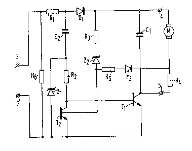
~ ig. 3 shows a first embodiment of the invention,
identical parts bearing the same reference numerals as in
Fig. 1. In this embodiment a resistor R4 i5 arranged in
series with the load M, the junction point between this
resistor R4 and the load M being connected -to the control
electrode of the transistor T2 via the series arrangement
of a zener diode Z3 and a resistor R5. These additional
elements constitute the first protection means which turn
off the power-supply circuit in the event of, for example~
1~ a short-circuit of the motor or blocking of the motor.
Above a specific value of the current through the load and
hence above a specific value of the voltage across the re-
sistor R~ the zener diode Z3 is turned on, so -that the
transistor T2 is turned on and consequently the transistor
T1 is turned off. The resistor R5 then limits the base
current of the transistor T2. During normal operation of
the circuit the protection means have another advantage.
If the transistor T2 turns off the transistor T1, the col-
lector voltage of the latter increases. This increase is
transferred to the base of the transistbr T2 via the re-
sistor R4,~the zener diode Z3 and -the resistor R5, re-
sulting in a positive-feedback effect which causes the
transistor T1 to be turned off very rapidly~
In this embodiment a negative voltage-dependent
resistor R6 is arranged between the input terminals 2 and
3 to limit the input voltage to, for example, 600 V.
Fig. 4 shows a second embodiment of the invention,
ln which identical parts bear the same reference numerals
as in Fig. 3. In this embodiment a resistox R8 is arranged
in the emitter line of the transistor T1 and the emitter
of the transistor T1 is connected to the base of the tran-
sistor T2 via the series arrangement of a resistor Rg and
a diode D2~ These elements constitute the second protec-
tion means which turn off the power-supply circuit in the
event of an excessive charging current through the tran-
sistor T1. If the power-supply circuit is switched on for
example at the instan-t at which the mains voltage has its
maximum value, the transistor T1 i5 turned on rapidly via
PH~T 11,52 7 16-07-86
the capacitor C2. At this instant the capacitor C1 is
stlll withou-t charge, so that a very large charging current
flows through the transistor T1 t which current is limited
only by the resistor R1. The transistor T1 is now protected
in that abDve a specific current the voltage across the
resistor R9 becomes so high that the transistor T2 is
turned on via the resistor Rg and the diode D2 and, con-
sequently, the transistor T1 is cut off. The resistor R9
then limits the base current of the transistor T2.
Fig. 5 shows a third embodiment of the lnvention,
in which identical parts bear the same reference numerals :
as in ~ig. 4. As the load of the motor M lncreases -the ca-
pacitor C1 is discharged to an increasing extent, so that
the average voltage across this capacitor decreases. This
causes the speed of the motor to decrease. In order to
maintain the speed of the motor as constant as possible at
increasing load, the average voltage across the capacitor
C1 should also increase at increasing load. For this pur-
pose the power-supply circuit comprises a correction cir-
cuit comprislng a transistor T3 whose base-emitter junctio
in series with a resistor Rlo, ia arranged in parallel with
the resistor R4 and whose collector is connected to the
cathode of the rectifier diode ~l via a resistor R11. The
series arrangement of the zener diode Z2 and the resistor
R3 is connected to the collector of the transistor T3. The
correction circuit operates as follows. As the motor cur-
rent increases and consequently the voltage across the re-
sistor R4 increases, the transistor T3 is driven ~urther
into conduction, causing the voltage across the resistor
R11 to increase further. As a result of this, the voltage
across the series arrangement of the resistor RL~, the
zener diode Z2 and the base-emitter junction of the tran-
sistor T2 decreases~ so tha~ this zener diode Z2 and the
transistor T2 are turned OIl at an increasingly higher in-
stantaneous value of the input voltage. Consequently, thetrans ~tor Tl is turned off at an increasing instantaneous
value of the input voltage~ so that the capacitor C1 is
charged to a voltage which increases as the load current
~7~
` ,~
P~L~ 11/52 8 lG-07-86
increases. A zener diode Z4 arranged in parallel with the
resistor R11 limits the voltage across the resistor ~11
above a speci~ic load curreIlt. This ensures that the vol-
tage across -the capacitor C1 cannot become higher than the
maximum permissible motor voltage at increasing load cur-
rent.
The invention is not limited to the embodiments
described herein but to those skilled in the art, many
modlficatlons are conceivable wlthin the scope of the pre-
sent inventlon. For example~ the first and the secondtransistor switch may comprise Darlington transistors or
other compound transistors. Instead of bipolar transistors~
fleld-effect transistors may be used~ in which case base,
collector and emitter should read gate, source and drain
respectlvely. Further, the zener diode Z1 may be replaced
by one or more serles-connected diodes. The first and the
second protection meaIls may also be constructed in another
manr.er and, in particular~ the current-sensing resistors
for measuring the load current and the charging current
may be arranged at other locations in the circuit. Fur-ther,
the transistor iIl the correction circult may be replaced
by any other amplifier circuit. Finally, it is to be noted
that the rec-tifier may alternatively comprise a full-wave
rectlfier or a bridge rectifier.