Note: Descriptions are shown in the official language in which they were submitted.
7~ 7
VLSI COAXIAL WIRING STRUCTURE
.
Technical Field
The invention relates to a shielded transmiss-
ion line structure fabricated in VLSI dimensions, as
well as to a.manufacturing ~ethod for making such a
structure.
, ' ' ,
Background Art
: ' '
In integrated circuit technology,. increasing
device density have lead to a decrease in the
spacing between adjacent metal lines. As metal
lines are formed closer together, the potential for
capacitive and inductiYe signal interference between
the lines increases. This interference is particu-
larly troublesome when high frequency signals are
propagated over adjacent lines.
. In the prior art, this problem has been dealt
with by const.ructing a metal line that is partially
or totally shielded by a metal structure surrounding
the metal line. A varying signal is propagated
along the metal line, and the metal structure is
coupled to ground potential. In combina~ion, the
two lines produce a ne~ligible external electro~a~-
netic field while also having a negligible suscepti-
bility to external fields from adjacent lines.
Examples of these prior art structures wil~ be re-
viewed in more detail.
. .
.~ .
~''
l~U9-8 6-0 19
,~,, ` - . ~ .
., . .~ . . . .
1~7~i7
There is a need in the art to develop a totally
shielded transmission line structure that is compatible
with current integrated circuit metallization
techniques.
Disclosure of the Invention
-
It is thus an object of the present invention to
provide a totally shielded transmission line structure.
It is another object of the invention to provide a
shielded transmission line structure that is compatible
with current integrated circuit metallization
techniques.
It is yet another object of the invention to
provide a shielded transmission line structure having
lateral dimensions in the micron range.
These and other objects of the invention are
realized by a coaxial wiring structure that is
constructed by depositing and etching a series of
conductor layers and insulator layers. More
specifically/ the shielded transmission line of the
invention comprises a first plate structure disposed on
a first insulator layer disposed on a substrate; a
second insulator layer disposed on the first insulator
layer and the first plate structure, the second
insulator layer having first troughs exposing end
portions of the first plate structure; a central
conductor and at least two peripheral conductors
disposed on the second insulator layer, the two
peripheral conductorsl and the central conductor/ the
third insulator layer having second troughs exposing
respective ones of the peripheral conductors; and an
upper plate structure formed on the third insulator
layer, the
BU9-86-019
3L~7~
-- 3 -- -
.
upper plate structure contacting the peripheral
conductors through the second troughs. In
combination, the upper plate structure, the
peripheral conductor structures and the lower plate
structure surround the central conductor and are
insulated therefrom by the respective insulator
layers. The surrounding conductors are coupled to
ground potential, and high frequency transmission
signals are propagated along the central conductor.
Brief Description of the Drawing
The foregoing and other structures and teach-
ings will be better understood upon a re~iew of the
description for carrying out the best mode of -the
invention as rendered belowO In the description to
follow, reference will be made to the accompanying
Drawing, in which:
- Fig. 1 (Prior Art) shows a cross sectional view
of a first partially shielded transmission line
known in the prior art;
Fig. 2 [Prior Art) shows a cut away view of a
second partially shielded transmission line known in
the prior art;
Fig. 3 (Prior Art) shows a cross sectional view
of a first totally shielded transmission line known
in the prior art;
, ~ .
Fig. 4 (Prior Art) shows a cross sectional view
of a second totally shielded transmission line known
in the prior art;
BU9-86-019
~q~ 7~6~
Fig. 5 (Prior Art) shows a cut away view of a
third totally shielded transmission line known in the
prior art;
Fig. 6 shows a cross sectional view of a first
embodiment of the totally shielded transmission line of
the present invention;
Fig. 7 - Fig. 9 show cross sectional views of a
substrate undergoing the process for forming the
shielded transmission line of the present invention as
shown in Fig. 6;
Fig. 10 shows a cross sectional view of a second
embodiment of the totally shielded transmission line of
the present invention; and
Fig. 11 shows a cross sectional view of a third
embodiment of the totally shielded transmission line of
the present invention.
BU9-86-019
7~
5 --
_
U.S. Patent 3,560,893 lissued 2/2~71 to Wen and
assigned to RCA Corp.) discloses a partially
shielded transmission line. As shown in Fig.
(Prior Art) the structure consists of a metal line
27 that is etched to define a central conductor 37
disposed on a dielectric substrate 25. A metal
capsule 23 is bonded to the etched conductor lines
27, and is coupled to ground potential so as to
partially shield inner conductor 37 from adjacent
lines. The inner conductor 37 is separated from the
outer conductors by air.
U.S. Patent 4,575,700 (issued 3/11/86 to Dalman
and assigned to Cornell Research Foundation, Inc.)
discloses a partially shielded "slot-line" transmis-
sion line structure. As shown in Fig. 2 (Prior
Art), conductive line 26B is deposited over a
portion of a silicon substrate that is defined by
two parallel grooves etched in the surface of a
silicon substrate. Adjacent conductive lines 26A,
26C are formed on the opposite surfaces of the
etched grooves, and the entire structure is
overcoated with a dielectric 28 so as to isolate the
lines from one another. Optionally, a third
conductive line 40 may be formed over the structure.
The conductive lines 26A, 26C and 40 are coupled to
ground so as to partially shield the inset conduc-
tive line 26B that is coupled-to a source of varying
potential.
U.S. Patent 3,370,184 (issued 2/20/68 to iule~g
and assigned to Hughes Aircraft Company) discloses
a totally shielded transmission line. As shown in
Fig. 3 (Prior Art), a pair of metal ~or doped
silicon) lines 2, 4 sandwich a central conductor 6
having a dielectric 23 disposed about its periphery.
BU9-86-019
Cadmium sulfide 8 separates the dielectric 23 from the
metal lines 2, 4. The metal lines are coupled to ground
and the central conductor receives a varying input signal.
U.S. Patent ~,581,291 (issued 4/8/86 to Bongianni and
unassigned on its face) discloses a micro-miniature
coaxial conductor. As shown in Fig. 4 (Prior Art), an
inner conductor 20 is formed of a copper wire having
lateral dimensions in the 100 micron range. The conductor
is then surrounded by a foamed dielectric 22 and a layer
of chemical vapor deposited (CVD) parylene. The entire
structure is then coated with an outer metal casing 24.
U.S. Patent 3,351,816 (issued 11/7/67 to Sear et al
and assigned to Bunker Ramo Corp.) discloses a planar
coaxial type structure. As shown in Fig. 5 (Prior Art),
aluminum plates lB, lC have a central aperture formed
therein that is filled with a dielectric material 5. In
turn, an aperture is formed within the dielectric material
5, and a conductive layer 7 is coated on the exposed
sidewalls of the aperture. The metal layer 7 defines a
through hole into which a wire 3 is inserted. The
aluminum plates lB, lC are coupled to ground potential,
and surround the central conductors 3, 7 so as to define
a coaxial structure.
Reference is made to the following patents for
further teachings of partially shielded transmission
BU9-8~-019 6
lines. USP 4,379,307 and USP 4,389,429 (issued 4/5/~3 and
6/21/83, respectively, to Soclof and assigned to Rockwell
International Corp.) disclose a conductive line that is
defined and a portion of a silicon substrate that is
subsequently etched so that the line is supported by a
series of support ridges. As a result, the conductive
line is isolated from adjacent conductors by air. USP
3,90~,995 (issued 9/9/75 to Stinehelfer Sr. and assigned
to Microwave Associates, Inc.) discloses a microwave
transmission line formed on a dielectric bod~ that is
bonded to a conductive material having a channel formed
therein. The conductive line lies within the channel,
such that it is separated from the ground plane by air.
The above prior art transmission line structures pose
several disadvantayeous features. In the prior art
structures shown in Figs. 1 and 2, note that there is no
electrical shielding provided below the central conductors
37 and 26B, respectively. While the prior art
transmission line structures shown in Figs. 3-5 do provide
total shielding, the methods of manufacturing these
structures are totally incompatible with current
metallization processing techniques. That is, these
structures would have to be formed before or after the
remainder of the chip is metallized.
BUg-86-019 6A
~71~67
Description of the Best Mode for Carrying Out the
Invention
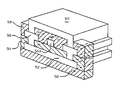
With reference to Fig. 6, a cross-sectional view
of totally shielded transmission line structure
compatible with current integrated circuit
metallization techniques is shown. Upper and lower
plate structures defined by conductor layers 60 and 52,
respectively, are coupled together by peripheral
conductor structures defined by conductor layer 52.
The peripheral conductor structures are disposed about
and spaced from a central conductor structure 56A.
High frequency signals are propagated along central
conductor 56A, and the outer conductors are coupled -to
ground potential. Note that the central
BU9-86-019
conductor 56A is separated from the conductors
- disposed about its periphery by insulator layers 54
and 58. As discussed below, the structure shown in
- Fig. 6 is constructed using state-of-the-art metal-
lization techniques. As such, the lateral length of
the central conductor of the present transmission
line is typically on the order of 0.5-10 microns.
The method of constructing the totally shielded
transmission line of the present invention will now
be discussed with reference to Figs. 7~9. As shown
in Fig. 7, a conductor 52 is defined on an insulator
layer 50. In general, layer 50 can be comprised of
any insulating material (silicon oxide, silicon
nitride, polyimide, doped glass, or combinations
thereof) typically utilized in the semiconductor
processing industry. Conductor 52 can be formed of
aluminum, aluminum alloys, refractory metals,
refractory metal alloys (e.g. silicides), doped
polysilicon, or various combinations thereof. In a
technology in which two layers of metal are used,
the lower conductor layer 52 can be comprised of the
same material ~and thus ~ormed at the same time) as
the electrodes of the devices (e.g. FET or bipolar
transistors, capacitors, etc.) formed elsewhere on
the silicon substrate. In the present invention,
this approach is preferred, and conductor 52 is made
of a refractory metal silicide ~such as tungsten
silicide) that defines the gate electrodes o~ the
FET devices. Conductor layer 52 can be subsequently
patterned using any conventional technique. In the
invention, it is preferred to cover the conductive
layer with a photosensitive polymer that is exposed
and developed to define the regions of conductive
layer 52 that are to be removed. These portions are
BU9-86-019
subsequently removed by exposure to an anisotropic
etchant that does not appreciable attach underlaying
portions of insulator layer 50. An example of such
an etchant would be a chlorine- or fluorine-based
gaseous plasma. After conductor layer 52 is
patterned, the structure is coated with insulator
layer 54. Similarly to the first insulator layer
50, insulator layer 54 can be comprised of any one
of a number of conventional insulating materials.
In the case where conductor layer 52 is formed
simultaneously with the electrodes of the active
devices provided elsewhere on the substrate,
insulator layer 54 is comprised of a doped glass
such as phosphosilicate ~lass (PSG) or borophos-
phosilicate glass (BPSG).
Then, as shown in Fig. ~, conductor layer 56 is
deposited and patterned to define a pair of periph-
eral conductors and a central conductor 56A. The
structure is formed by first etching troughs holes
in insulator layer 54 to expose end portions of the
patterned conductor layer 52. A photosensitive
polymer is deposited and patterned so as to expose
selective portions of insulator layer 54 to an
anisotropic etchant (e.g. CF4/O2 directional plasma)
without appreciahly attacking underlaying portions
of conductor layer 52. It is to be understood that
such troughs can be etched to provide an isotropic
profile to the etched troughs. Then, conductor
layer 56 is deposited so as to fill the troughs
holes formed in conductor layer 54, and is patterned
to produce the structure shown in Fig. 8. Note that
while conductor layer 56 can be composed of the same
materials discussed with reference to conductor
layer 52, in practice it is preferred to form
conductor layer 56 from a material that can be
chemically vapor deposited (CVD) so as to fill the
BU9-86-Olg
7~67
--10--
troughs formed in insulator layer 54 without
-- creating voids. It has been found that refractory
metal layers such as tungsten provide good trough
filling properties. Note that after patterning, the
peripheral conductors are separated from and
disposed about the central conductor 56A.
After conductor layer 56 is deposited and
patterned as shown in Fig. 8, another insulator
layer 58 is deposited on the structure. Insulator
layer 58 can be formed from any conventional
insulating material. Similarly to insulator layer
54, insulator layer 58 is then patterned by exposure
of selected portions thereof (as defined by a
photoresist layer PR2) to an anisotropic plasma etch
that remov~s the exposed portions without appreci-
ably etching underlaying portions of conductor layer
56. Note that the pattern defined by photoresist
PR2 must be aligned with respect to the underlaying
layers, so that the troughs etched into insulator
layer 58 exposed portions of the peripheral
conductors 56 without exposing central conductor
56A. In practice, this alignment can be made less
critical by lengtnening the portions of peripheral
conductors 56 that are disposed along the upper`
surface of insulator layer 54. After the troughs
are formed in insulator layer 58, photoresist PR2 is
removed and metal layer 60 is deposited and etched
in a manner similar to that utilized to provide
conductor layer 56l resulting in the structure shown
in Fig. 6.
Fig. 10 shows a second embodiment of the
present invention, wherein separate metal layers are
used to fill the troughs defined in insulator layers
54 and 58. That is, instead of using a single metal
BU9-86~019
deposition to both fill the troughs hole dfined in the
insulator layer and define a metal line on the upper
surface of the insulator layer, separate metal layers
are provided. As shown in Fig. 10, the troughs formed
in insulator layers 54 and 58 are filled with metal
layers 53 and 57, respectively. Thus, the peripheral
conductors are defined by conductor layers 53 and 56,
and the upper plate structure is defined by conductor
layers 57 and 60. In practice, a CVD material such as
tungsten is used for its gap filling properties. One
or both of the metal layers 56 and 60 can now be formed
from a material (such as aluminum) that provides
optimum conductivity properties, without these gap
filled considerations.
Fig. 11 shows a third embodiment of the present
invention, where a series of insulator layers are
utilized to define the conductive structures.
Insulator layer 54 is deposited on lower plate
structure 52, and an insulator layer 55 is deposited
thereon. The two :insulator layers 54 and 55 are
sequentially etched to define troughs as shown. Note
that at least some of the troughs in layer 55 are
formed above (and are wider than) the troughs formed in
layer 54. The troughs in layer 55 define upper
portions of the peripheral conductor structures as well
as the central conductor structure. The conductive
material 56 is then deposited to fill the respective
troughs, and is planarized so that portions of the
conductive material above the upper surface of
insulator layer 55 are removed. This planarization
procedure is taught in published European Patent
Application 224,013, filed October 17, 1986 by Chow et
al, entitled "Method for Producing Coplanar Multi-Level
Metal/Insulator Films on a Substrate and for Forming
Patterned
BU9-86~019
6~
Conductive Lines Simultaneously with Stud Vias," filed
October 28, 1985, and assigned to the assignee of the
present invention. Insulator 58 is then deposited over
the conductor 56, and another insulator layer 54 is then
deposited thereon. A large trough is defined in insulator
layer 59, to span over the smaller troughs formed in
insulator layer 58. Then conductor layer 60 is deposited
and planarized to fill the troughs in insulator layers 58
and 59 to form the upper plate structure.
As shown by the foregoing description, a first feature
of the invention is that it provides a totally shielded
transmission line of integrated circuit dimensions.
A second feature of the invention is that the shielded
transmission line can be processed concurrently with the
metallization layers used to interconnect the various
devices formed on the semiconductor substrate.
It i~ to be understood that while various
modifications to the structure and teachings described
above may occur to a person of ordinary skill in the art,
such modifications fall within the spirit and scope of the
present invention.
BU9-86-019 12