Note: Descriptions are shown in the official language in which they were submitted.
155(~
SEMICONDUCTOR LIGHT EMITTING DEVICE
WITH VERTICAL LIGHT EMISSION
BACKGROUND OF THE INVENTION
1. Field of the Invention
This invention generally relates to a light
emitting device, and, in particular, to a semiconductor
light emitting device, such as a light emitting diode or
semiconductor laser, for emitting light in~a direction
perpendicular to a main surface of a substrate. More
specifically, the present invention relates to a
semiconductor laser device capable of emitting a laser
beam in a vertical direction with respect to a main
suriace of a substrate.
2. Description of the Prior Art '
A semiconductor light emitting device, such as
a light emitting diode or semiconductor laser, is well
known in the art, and it generally includes a
l semiconductor substrate in which one or more PN junctions
are provided to define an activation region for emitting
light. A semiconductor light emitting device capable of
emitting light in a vertical direction with respect to a
main surface of a substrate is also known and this type
of semiconductor light emitting diode is preferred
because it can be easily coupled to a light transmitting
element, such as an optical fiber, and it has various
possible applications, such as a display device.
~7~L5~
The activation region typically has a thickness
in the order of 2 - 3 microns. As a result, and as will
be explained hereinafter in greater detail, in order to
attain sufficiently large gain in the intensity of light
emitted in a direction vertical to the main surface of the
substrate, an extremely large injection current density is
required. Since the activation layer extends laterally or
in parallel with the main surface and the light emitting
function takes place across the enltire activation layer,
the light emitted in the direction perpend;cular to the
main surface of the substrate is lower and limited in
light intensity.
SUMMARY OF THE INVENTION
A light emitting device according to the
invention comprises a substrate having a first surface and
a second surface which is oeposite thereto. The substrate
is provided with a through hole extending between the
first and second surfaces. An active area is defined in
the substrate extending in parallel with a side wall of
the through hole, such active area generating light when
current flows therethrough. A pair of first and second
electrodes are formed on the substrate on opposite sides
of the active area for passing current through the active
area. Pceferably. the side wall is substantially
pereendicular to at least one of the first and second
surfaces and, more ereferably, the first and second
surfaces are parallel.
In yet a further preferred embodiment of the
invention, the through hole has a recess at one end, which
is si2ed to receive one end of an optical fiber.
Also, according to the invention, there is erovided an
array type light emit~ing device~ comprising a substrate
having a first surface and a second surface which is
opposite thereto, the substra~e being provided with a
plurality of through holes arranged in the form of an
-- 2 ~
1~7~5~
array, each o~ which extends between the first and second
surfaces. A plurality of active areas are formed in the
substrate, each extending in parallel with a side wall of
a corres~onding one of the plurali~y of through holes,
these active areas generating light when curren~ flows
therethrough. A pair of first and second electrodes are
formed on the substrate for passing cu~rent through the
active areas.
other objects, advantages and novel features of
the present invention will become apparent from the
following detailed description of the invention when
considered in conjunction with the accompanying drawings.
BRIEF DESCRIPTION OF T~E DRAWINGS
Figs. 1 and 2 are schematic, cross sectional
views showing two typical prior art semiconductor light
emitting devices capable of emitting light in a vertical
direction;
Figs. 3 through 5 are schematic, cross
sectional views showing several semiconductor light
emitting devices constructed in accordance with the
present invention;
Fig. 6 is a schematic, perspective view showing
a semiconductor light emitting array device constructed
in accordance with a further em~odiment of the present
invention;
~155~
Fig. 7 is a schematic, cross sectional view
showing a semiconductor light emitting device constructed
in accordance with a still further embodiment of the
present invention, wherein one end of an optical fiber îs
fitted into a receiving hole formed in one surface of a
substrate;
Fig. 8 is a schematic, cross sectional view
showing a semiconductor light emitting array device
constructed in accordance with a still further embodiment
of the present invention using the structure shown in
Fig. 7;
Fig. 9 is a schematic, cross sectional view
showing another typical prior art semiconductor light
emitting device capable of emitting light in a vertical
direction;
Fig. 10 is a schematic, perspective view
showing a semiconductor light emitting device for
emitting light in a vertical direction constructed in
accordance with a still further embodiment of the present
invention;
- Fig. 11 is a schematic, cross sectional view of
the device shown in Fig. 10;
- Figs. 12a through 12c are schematic, cross
sectional views showing steps in a process for
manufacturing the device shown in Figs. 10 and 11;
- 4 -
Figs. 13 through 16 are schematic, cross
sectional views showing several modified strNctures;
Fig. 17 is a schematic, cross sectional view
showing a semiconductor laser for emitting light in a
vertical direction constructed in accordance with one
embodiment of the present invention;
Fig. 18 is a fragmentary, cross sectional view
showing on an enlarged scale that portion of the
structure shown in Fig. 17 which is encircled by A;
Fig. 19 is a schematic, cross sectional view
! showing a semiconductor laser for emitting light in a
vertical direction constructed in accordance with another
embodiment of the present invention;
Fig~ 20 is a fragmentary, cross sectional view
showing on an en~arged scale that portion of the
structure shown in FigO 19 which is encircled by B; and
Fig. 21 is a schematic, cross sectional view
showing an array type semiconductvr light emi-ting device
constructed in accordance with a still further embodiment
of the present invention.
Figs. 1 and 2 show typical prior art
semiconductor light emitting devices capable of emitting
light in a vertical direction. A light emitting device
shown in Fig. 1 includes a semiconductor substrate 2
having an electrode 1 attached to its bottom. The
substrate ? includes a p-AlGaAs layer 21, a p-AlGaAs
activation layer 3 and an n-AlGaAs layer 22 from bottom
to top, and another electrode 5 circular in shape is
_ 5 _
5~)
provided on the layer 22. On the other hand, Fig. 2
shows a prior art light emitting device which încludes a
semiconductor substrate 2 having a bottom electrode
attached to the bottom thereof. The substrate 2 includes
an n-GaAs layer 24, an n-GaAsP graded layer 25 and an
n-GaAsP layer 26 from bottom to top, and a circular top
electrode 5 having a light emitting opening 51 is
provided on layer 26. And, an activation layer 3 is
formed inside of the n-GaAsP layer 26 at a location
immediately below the light emitting opening S1.
As is obvious from Figs. 1 and 2, even if it is
of the vertical light emitting type, any prior art
semiconductor light emitting device includes one or more
PN junctions defined in a substrate to define an
activation region, where the light-emitting phenomenon
takes place, as extending in parallel with a main surface
thereof, which is a surface having a larger area. And,
the activation region typically has a thickness in the
order of 2 - 3 microns. As a result, in order to attain
a sufficiently large gain in the intensity of light
emitted in a direction vertical to the main surface of
the substrate, an extremely large injection current
density is required. Since the activation layer 3
extends laterally or in parallel with the main surface
and the light emitting function takes place across the
entire activation layer 3, the light emitted in the
direction perpendicular to the main surface of the
substrate is lower and limited in light intensity.
- 6 -
s~
DESCRIPTION OF THE PREFERRED EMBODIMENTS
Referring now to Fig. 3, there is schematically
shown a semiconductor light emitting device constructed
- in accordance with one embodiment of the present
invention. As shown, the present device includes a
7 -
5SI)
semiconductor substrate 2 which is generally rectangular
or circular in shape in the illustrated example and which
has a pair of top and bottom main surfaces which are
relatively large in area. The substrate 2 is provided
with a through hole 4 extending in a direction
perpendicular to the pair of top and bottom main surfaces
of the substrate 2. An active region 3 is defined in ~he
substrate along a side wall 41 of the hole 4, and the
active region 3 is typically defined by introducing an
impurity material, such as Zn, into the substrate 2
through the side wall 41 to a predetermined depth. When
introducing the impurity material into the substrate 2
;through the side wall 41, it is also introduced into the
- i
substrate 2 through the bottom main surface, so that the'
active region 3 of the illustrated embodiment includes
not only a vertical active region 31, but also a
horizontal active region 32. It is to be noted that the
horizontal active region 32 is not always necessary from
- the view point of the present invention, and, thus, the
present~ ght emltting device-may also be structured
without the horizontal active region 32, if desired. It
should also be noted that, as well known in the art, the
active region is a region in which recombination between
holes and electrons take place to thereby emit light.
25A bottom electrode 1 is formed on the bottom
main surface of the substrate 2 and also on the side wall
7155~
41 continuously. On the other hand, a top electrode 5 in
the form of a ring or having a circular opening 51 larger
in diameter than the outer diameter of the vertical
active region 31 is formed on the top main surface of the
substrate 2. The opening 51 formed by the top electrode
5 defines a light Qmitting opening through which the
light emitted from the vertical active region 31 is lead
out to the exterior. The substrate 2 may~be comprised of
a material selected from a group consisting essentially
- 10 of GaAS, AlGaAs, InP, InAsP and InAsSb~, which are Group
III-V compound semiconductor materials, from a group
consisting essentially of ZnSe, æns, ZnO, CdSe and CdTe,
which are Group II-VI compound semiconductor materials,
or from a group consisting essential of PdTe, PdSnTe and
PdSnSe, which are Group IV-VI compound semiconductor
materials.
It is to be noted that although the term
"vertical" is used to denote the active region defined
adjacent to the side wall 41 of the through hole 4, thè
active region 31 should not be limited only---to the case
in which the active region 31 extends at right angles
with respect to the top main surface. The vertical
active region 31 may be inclined inwardly or outwardly
with respect to the main top surface, which is the
surface through which emitted light is lead out to the
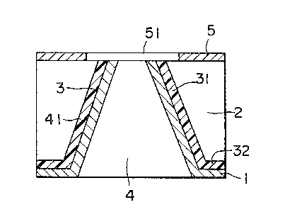
exterior, of the substrate 2. Fig. 4 shows a modified
~'7~55~)
structure in which the through hole 4 def ined in the
substrate 2 has a truncated conical shape, so that the
side wall 41 of the hole 4 and thus the vertical active
region 31 formed along the side wall 41 is inclined with
respect to the center line of the through hole 4. Other
; than the fact that the through hole 4 has a truncated
conical shape and thus the active region 31 is inclined
O with respect to t~e top main surface of the substrate 2,
the remaining structure remains the same as that shown in.
10 Fig. 3. With this structure, the light emitted is
convergent in the direction of travel.
Fig. 5 shows a semiconductor light emitting
device constructed in accordance with another embodiment
of the pxesent invention. Similarly with the structure'
shown in Fig. 3, the present device also includes a
semiconductor substrate 2 which also has a pair of top
~ .
and bottom main surfaces and a through hole 4 extending
vertically or substantially vertically with respect to
th~e--top main surface. The susbtrate 2 is provided wi-th a
vertical activç region 31 formed along the side wall 41
of the through hole 4 and no horizontal active region is
provided in the subsrate 2 of this embodiment. Instead,
an electrically insulating layer 21 is formed on the
bottom main surface of the substrate 2, for example, from
SiO2 or SiN4. With the provision of this insulating
layer 21, when a selected impurity material is diffused
- 10 --
-
55~
into the substrate 2 through the side wall 41 to form the
lateral active region 31, the insulating layer 21 serves
as a mask thereby preventing thé impurity material from
being diffused into the suhstrate 2 through the bottom
main surface thereof. Thus, no lateral or horizontal -
active region is formed in the substrate 2 of this
embodiment. In addition, a bottom electrode 1 is formed
as e~tending on the insulating layer 21 and being plugged~
.. . ....................................... .
' into the through hole 4. A top electrode 5 having a
circular opening 51 is formed on the top main surface of
the substrate 2. Thus, the opening 51 defines a light
emitting opening through which the light emitted from the
vertical active region 31 is lead out to the exterior.
' It should be notad that the column section of the bottom~
electrode 1 plugging the through hole 4 also serves as a
heat sink for dissipating heat produced by the active
region 31 thereby maintaining the active region 31
~ relatively at constant temperature.
; -- As is-~obvious--for one skilled in the art, the
,. . .. . .
l~onger'the~longitudinal length of the''vertical active ~
.
region 31, the larger the gain of output light in the
vertical direction, i.e., direction perpendicular to the
main top surface of the substrate 2, where the light
emitting opening 51 is provided. As a result, in order;
to provide a high power light emitting device, it is
` preferable to use the substrate 2 whose thickness is as
~ 2~
large as possible. For example, the thickness of the
substrate 2 is set at least at 10 microns, or preferably
at least at 20 microns, more more preferably at least at
100 microns.
S Fig. 6 shows an array type semioonductor light
emitting device using one of the structures shown in
Figs. 3 and 4. This embocliment may b~ fabricated by
s providing a plurality.of through. holes.~4 in a single l
.: substrate 2 in the form of a two dimensional array, for .
example, by etching, introducing a selected impurity
material into the substrate 2 at least through the side
wall of each of the plurality of through holes 4, and
then forming a pair of top and bottom electrodes 5 and 1
on the top~-and bottom main-surfacës of the substrate 2.'
lS As a modification, the top electrode 5 may be subdivided
such that each subdivided section is unique to the
corresponding through hole 4, in which case the plurality
of vertical active regions 41 may be activated
individually, so that such a modified structure may be
.
20 used as.a.display .unit. Besides,-.the structure shown.~in
Fig. S may also be applied to form an array device as
shown in Fig. 6.
As described above, the basic structure of the
present invention requires the ~ormation of a through
hole extending vertically or inclined with respect to at
least one main surface of the substrate. And, such a
- 12 -
5~
through hole can be easily formed at high precision by
various techniques well known for one skilled in the art,
for example, the reactive ion etching technique.
Besides, the vertical active region 31 can also be easily
formed, for example, by diffusion of a selected impurity
material, such as zn. Thus, the structure of the present
- --- inventlon can be fabricated with ease using the
conventional semiconductor manufacturing techniques, so
that the present device can be fabricated at low cost
because it does not require expendi~ure of capital or
facility cost.
It should also be noted that the characteristic
b tween the emitted light intensity and the length of
.~ .. ,1~ ,-
active region is linear for a light emitting diode having
the length of active region in the order of a few
` microns. However, if the active region is relatively
-- - long, the light generated by induced emission increases
~- spontaneous emission as it propagates along the active
region, thereby providing an ampl'ified spontaneous light
emission. As described above, in accordance with the
principle of the present invention, since there can be
- - ~ provided a relatively long vertical active region, for
. . .
example, of 10 microns or more simply by using a
substrate 2 having a desired thickness, so that a high
gain of light output in the vertical direction can be
obtained quite easily.
- 13 -
7~55~)
Referring now to ~ig. 7, there is schematically :
shown in cross section a semiconductor light emitting
device constructed in accordance with a further
embodiment of the present invention. As shown, the
present device includes a plate-shaped substrate 2 which
has a pair of opposite top and bottom main surfaces and
which is provided with a through hole 4 extending through
the substrate 2. A circular recess 6 is formed in the
top main surface of the substrate 2 to a predetermined
depth and the diameter of the circular recess 6 is sized
to receive therein one end of an optical fiber 7. In the `~
illustrated embodiment, the recess 6 has a flat surface
which is generally in parallel with the top main surface
of the substrate 2. The through hole 4 extends from the
bottom surface of the recess 6 to the bottom surface of
the substrate 2 and it is defined by a side wall 41. An
active regions 31 is formed in the substrate along the
side wall 41 by causing a selected impurity material,
such as Zn, to be diffused into the substrate 2~through
the side wall 41. Thus, light is emitted in the active
region 31 and propagates along the longitudinal direction
of the through hole 4 to be lead into the optical fiber
7.
A bottom electrode 5 having a circular opening
is formed on the bottom surface of the substrate 2, and
another electrode 1 is formed on the side wall 41 of the
j,
,
~ '
7~ 5~
through hole 4 and on the bottom surface of the substrate
2 around the periphery of the bottom end of the through
hole 4. The bottom end of the optical fiber 7 is
preferably cemented into the recess 6. Thus, the top end
of the active region 31 defines a light emitting opening,
through which emitted light is introduced into the
optical fiber 7. By suitably sizing the diameter of the
~ receiving recess 6, the.. bottom end of t~e optical fiber 7 ..
.. . . ... ... .
: may be simply press-fitted into the recess 6 so as to .--
10 have the bottom end of the optical fiber 7 fixedly :.
attached to the light emitting opening 51, if desired.
In the illustrated embodiment, the active region 31
extends perpendicular to or substantially perpendicular
, - , ,
to the bottom surface of the recess 6; however, the ' ~.
active region 31 may also be so formed to be conically
upwardly or downwardly, as desired. In the Iatter case,
the active region 31 is inclined with respect to the
bottom surface of the recess 6. The depth of the
receiving recess 6 is preferably set in a range between
approximately 500 microns and approximately 2 mm.
Fig. 8 shows in perspective view-an array type
light emitting device constructed in accordance a still
further embodiment of the present invention using the
structure shown in Fig. 7 as a unit element. That is, as
shown in Fig. a, the light emitting element shown in Fig.
: 7 is defined in the substrate 2 in the form of a two
- 15 --
lS~
dimensional array. In this embodiment, each light
emitting element has an individual electrode 1 because it
is mainly formed on the side wall 41 of each through hole
4. Thus, using the bottom electrode 5 as a common
electrode, the plurality of light emitting elements
defined in the same substrate 2 can be controlled
individually in operation. Such a structure is
i particularly advantageous when applying the present
invention to a display apparatus.
Now, another aspect of the pxésent invention
will be described. First, `referring to Fig. 9, another
prior art semiconductor laser device which emits a laser
beam in a vertical direction will be~ described. The
~- laser device shown in Fig. 9 includes a first
semiconductor layer 101 having a first conductivity type,
a second semiconductor layer 102 having a narrower
forbidden band gap than that of the first layer 101 and
serving as an active layer and a third semiconductor
layer 103 formed-on the -second-semiconductor layer 102
: - 20 and having a second conductivity type-, which is- oppositein polarity to the first conductivity type, and a broader
forbidden band gap than that of the second layer 102. In
addition, on the third semiconductor layer 103 is formed
fourth and fifth semiconductor layers 104 and 105 one on
top of another in the order mentioned. On the other
hand, at a selected portion of a bottom surface of the
. , .
- 16 -
1~73LS5~)
first semiconductor layer 101 is formed an electrode
semiconductor layer 106 of the first conductivity type
and a silicon dioxide layer 107 is formed on th~
remaining bottom surface of the first semiconductor layer
. - 5 101. Moreover, an electrode metal layer 108 is formed~on -~
' these layers 106 and 107 and this metal layer 108 also:
serves as a reflecting mirror.
As shown, a recess is formed as~.extending -~
'' through the fourth and fifth'semiconduckor layers 104 and :
105, and the bottom of this recess is coplanar with~.thë~
interface between the layers 103 and 104. On the top~ .
surface of the fifth semiconductor layer 105 is formed an
' electrode metal layer 109 of the second conductivity
" type, and a reflecting electrode layer 110 is formed'on'
15 the electrode metal layer 109 and also on the side and
bottom walls of the recess.
With the above-described structure, -when
~; current is supplied to flow between the top and bottom
- - electrodes 108 and 10-9, thecurrent flows in the ~
-- - ., -
~-- - 20 direction indicated by the .arrows 131, so that th=~e
current 131 mainly flows through an active region or
light emitting portion 102a of the second semiconductor
layer 102, thereby causing light to be emitted, whereby
the light thus emitted is confined between the el~ctrode
25 metal layers 108 and 109, which also serve as reflecting
'~' mirrors, so that laser oscillation takes place and thus a
1~71S~O
laser beam 130 is emitted to the exterior i~ a vertical
direction perpendicular to the plane or main surface of
the device.
In such a prior art vertical emitting type
semiconductor laser device, since carriers are confined
in the active region, the thickness of the semiconductor
layer 102, which defines the active region, must be set
equal to or less than the di~fusion length of carriers,~
which is approximately 2 - 3 microns. As a result, there
~; 10 is a limit in the gain of a laser beam emitted in the ~
vertical direction because the thickness of the active -
region cannot be made larger. It i5 true that the laser
output can be increased by increasing the level of
- current, but this is disadvantageous because it causes' --~ '
other problems. In addition, in the structure shown in~
Fig. 9, the top electrode lO9 at the beam output side is
annular in shape, so that the injected current tends to
flow sideways as indicated by the arrows 131. Thus, in
- this structurè~, it is difficul~ to produce current
~ 20 concentration.- In addition, since the light emitting -
.
portion 102 extends laterally, the current injection
efficiency into the active region 102a tends to be
reduced. For these reasons, when operating such a prior
art device as a laser, it is extremely difficult to lower
the threshold current and also to increase its output
' power.
.
- 18 -
7~5SO
In accordance with this aspect of the present
invention, there is provided a semiconductor light
emitting device which compxises a substrate having one
surface on which a semiconductor layer is formed, said
semiconductor layer being provided with a recess
extending from an outer surface of the semiconductor
layer toward the substrate and an PN junction being
~; formed in the semiconductor layer extending along the
side wall of the recess. With this structure, current is-
caused to flow across the PN junction, thereby causing
recombination of electrons and holes in the vicinity of
the PN junction, so that light is emitted in a direction
, perpendicular or substantially perpendicular to the
- surface of the substrate or device. As described with
respect to the previous embodiments, such a PN junction
`c is preferably defined by causing a selected impurity
material to be thermally diffused into the semiconductor
layer from the outside surface.
Now, referring to Fig. 10, there is shown in
20 perspective a semiconductor light emitting device
constructed in accordance with one embodiment of this
aspect of the present invention. And, Fig. 11 is a cross
sectional view of the device shown in Fig. 10. As shown,
the device includes an n-GaAs substrate 111, an n-AlGaAs
25 layer 112, an n-GaAs layer 113, a p-AlGaAs layer 114 and
an n-GaAs layer 115 overlying on top of another in the
-- 19 --
order mentioned. It is to be noted that the structure
including all of these layers 111 through 115 is also
referred to as a substrate. And, importantly, a recess
120 circular in shape in the illustrated embodiment is
provided extending vertically through the layers 113, 114
and 115. Thus, the recess 120 extends generally
vertically with respect to the top surface of the
substrate 111 and the bottom surface of the recess 120 is
coplanar with the interface between the layers 112 and .
113. In the present embodiment, the recess 120 is
cylindrical in shape; however, it may have any other
shape, such as a conical shape, and the recess 120 also
may have any other desired cross sectional shape than a
circular shape as shown.
A selected impurity material, preferably Zn, is
~; diffused into the present structure through the side and
bottom walls of the recess 120 and the top surface of the
layer 115, so that a p type diffusion region 116 and a p+
diffusion region 117 are defined. A p type electrode
layer 118 is formed on the n-GaAs layer 115; on the other
hand, an n type electrode layer 119 is formed on the
bottom surface of the substrate 111, which is formed with
a counter recess llla in alignment with the recess 120
and reaching to the interface between the n-AlGaAs
semiconductor layer 112 and the substrate 111. As will
` be described later in detail, in the present embodiment,
- 20 -
~7155~)
light emitted is taken out in the direction indicated by
the arrow 121.
It is to be noted that the PN junctions formed
in the n-GaAs layer 115 as extending in parallel with the
top surface of the substrate 111 are separated away from
the p-AlGaAs layer 114. 'rhus, a pnpn structure is
defined by the p type diffusion region 116, n-GaAs layer
115, p-AlGaAs layer 114 ancl n-GaAs layer 113. For this
reason, this pnpn structure serves as a current flow
blocking structure for the current flowing between the
top and bottom electrode layers 118 and 119. As a
result, the current flowing between the top and bottom
electrode layers 118 and 119 is forced to flow
preferentially along the side wall of the recess 120 and'
thus along the pn junction extending perpendicular to the
.~ top surface of the substrate 111. Accordingly, at and in
the vicinity of the pn junction extending vertically
along the side wall of the recess 120, recombination of
electrons and holes takes place to emit light which is
mainly guided to the exterior through the bottom recess
llla defined as a light outlet. Therefore, the vertical
pn junction extending along the side wall of the recess
120, in effect, defines an active region for emitting
light.
As described above, in accordance with the
structure of the present embodiment, since the pnpn
- 21 -
.
~7~55~
structure serves as a current blocking structure, the
current flowing between the top and bottom electrodes
mainly passes across the pn junction extending in
parallel with the side wall of the recess 120, the
current injection efficiency is significantly enhanced.
Furthermore, with this structure, a heat sink tnot shown)
may be mounted on the top electrode layer 118 so that the
heat sink may be placed close to the active region,
thereby allowing to enhance the heat dissipating
characteristic and to obtain a high light output. In
addition, in accordance with this structure, the pn
junction defining the active region can be set as long as
possible in th~ direction of light emission, thereby
permitting to enhance the directionality by narrowing thé
angle of divergence of emitted light. Moreover, as will
be described more in detail later, by providing a pair of
reflecting mirror elements so as to sandwich the active
region therebetween, there can be easily defined a
vertical light emitting type laser having an increased
gain. ~In the structure shown in Fig. 11, the recess 120
has a bottom wall defined by the surface of the layer
112; however, as an alternative structure, the bottom
wall of the recess 120 may be defined within the layer
113, if desired.
Now, with reference to Figs. 12a through 12c, a
method for manufacturing a semiconductor light emitting
- 22 -
y~
: `
LS5~)
device having the structure shown in Figs. 10 and 11 will
be described. As shown in Fig. 12a, on an n-GaAs
substrate or base layer 111 is formed an n-AlxGa~ xAs
layer 112 (where, x is a mole fraction of Al and in a
range between 0.2 and 0.45) to the thickness between 2
and 100 microns, an n-GaAs layer 113 to the thickness
between 2 and 100 microns, a p AlxGal xAs layer 114
(where, x is in a range between 0 and 0.4) to the
thickness between 0.5 and 3 microns and an n-GaAs layer -
115 to the thickness between 3 and 10 microns in the
order mentioned from bottom to top. Then, as shown in
Fig. 12b, after forming an electrically insulating layer
122 on the layer 115, an opening is formed in the
insulating layer by photolithography. The insulating
layer 122 is preferably comprised of a material, such as
silicon oxide, silicon nitride, or resist. Using this
insulating layer 122 with a hole as mask, a recess 120 is
formed by dry etching until its bottom reaches the
n-AlGaAs layer 112. This recess 120 may have any desired
cross sectional shape, such as a circle, a rectangle or
any other polygonal shape. As the dry etching technique,
use is preferably made of reactive ion etching using a
mixture gas containing chlorine gas and Ar gas.
Then, as shown in Fig. 12c, after removing the
mask 122, thermal diffusion is carried out using 2a as an
impurity dopant, thereby forming a p type diffusion
- 23 -
.: , . .
7~5~3
region 116 and a p diffusion region 117 along the side
and bottom walls of the recess 120 and the top surface of
the n GaAs layer 115. In this case, preferably use is
made of a two-step diffusion method. Furthermore, this
diffusion step should be so controlled that the diffusion
front defined by the diffusion of the impurity dopant
introduced through the top surface of the n-GaAs layer
115 does not reach the underlying p-AlGaAs layer 114.
Thereafter, a pair of top and bottom electrode layers is -
formed on the top and bottom surfaces and then a bottom
recess llla is formed in the substrate 111 by etching,thereby completing the structure shown in Figs. lO and
ll. The etching to form the bottom recess llla may be
,
preferably carried out by wet etching using an etchant
oontaining ammonia and a solution of hydrogen peroxide.
Such an etchant attacks GaAs but not AlGaAs, so that the
etching automatically stops as soon as the n-AlGaAs layer
112 is exposed.
Fig. 13 shows a semiconductor light emitting
device constructed in accordance with another embodiment
of the present invention. Since this device has
basically the same structure as that of the previous
embodiment shown in Figs. 10 and 11, like numerals
indicate like elements and the description of the same
elements will not be repeated. In the present
embodiment, instead of the pnpn structure, an
- 24 -
1~'7155~3
electrically insulating layer 122 is formed on the n-GaAs
layer 113 and this insulating layer 122 serves as a
current blocking structureO In addition, in the present
structure, the 2n-diffused regions 116 and 117 are formed
only along the side and bottom walls of the recess 120.
And, a p type metal electrode layer 118 is formed not
only on the insulating layler 122, but also on the inner
side wall of the recess 120. That portion of the p type
metal electrode layer 118 which is located within the
recess 120 is indicated by 118a. Thus, also in the
present embodiment, the current flowing between the top
and bottom electrodes 118 and 119 is forced to flow
preferentially across the pn junction extending
vertically with respect to the top surface of the
substrate 111, so that the current injection efficiency
to the active region is significantly increased.
~ ith this structure, the insulating layer mask
122 used as an etching mask when forming the recess 120
by dry etching is~also used as a diffusion mask when
carrying out diffusion of Zn, and, urthermore, the
insulating layer 122 also serves as an electrical
insulation between the electrode 118 and the n-G~As layer
113. As a result, the manufacturing process is extremely
simplified. Similarly with the previously described
embodiment, this embodiment also allows to obtain a high
- 25 -
' J ~7155~
light output power and to prevent the emitted light beam
from becoming divergent.
Fig. 14 shows another embodiment of the present
invention, which is a modification of the structure shown
in Fig. 13. Thus, the present embodiment is structurally
similar to the embodiment shown in Fig. 13 in many
respects; however, in the present embodiment, the
diffusion regions 116 and 117 are formed not only along
the side and bottom walls of the recess 120, but also
along the top surface of the n-GaAs layer 113. In the
present embodiment, the insulating layex 122 is not used
as a diffusion mask when carrying out the Zn diffusion
step, and it is formed after the Zn diffusion step.
Fig. 15 shows a further embodiment of the
; 15 present invention, which is similar in structure to the
'~.t,., embodiment shown in Fig. 13 in many respects. In this
:
embodiment, however, the recess 120 is plugged with the
same material as that of the electrode layer 118, thereby
defining a plugging portion 118b s~rving as part of a
heat sink. With this structure, the heat sink 118 can be
located very close to the active region extending
perpendicular or substantially perpendicular to the
surface of the substrate 111 so that the heat dissipating
characteristic is significantly improved. In the present
embodiment, an insulating film 122a is formed on the
bottom wall of the recess 122, so that the electrode 118
- 26 -
1~71S~
and 118b is not in electrical contact with the layer 112
directly. Fig. 16 shows a still further embodiment of
the present invention, which is also very similar in
structure to the device shown in Fig. 13 excepting the
fact that the recess 122 is filled with a heat conductive
resin material 123 so as to provide an enhanced heat
dissipating characteristic. It is to be noted that the
~,~ resin 123 may be replaced by polisilicon, if desired.
Figs. 17 through 20 show embodiments when the
present invention has been applied to a laser. Fig. 17
shows a vertical light emitting type semiconductor laser
constructed in accordance with one embodiment of the
present invention and Fig. lB shows the detailed
structure of that portion which is surrounded by a circlé
A. In the present embodiment, on the n-AlGaAs layer 112
x, is formed a laminate layer 124, which, as shown in Fig.
18, is formed by overlying an n-GaAs layer 126 and an
AlGaAs layer 127 one on top of another alternately over a
predetermined number of times. The thickness of each of
the layers 126 and 127 is set at 1/4 of an equivalent
value of wavelength within the GaAs or AlGaAs layer 126
or 127 converted from the wavelength of emitted light.
As a result, there is provided a so-called Distributed
Feedback (DFB) structure. With the provision of such a
DFB structure, there is provided optical resonators for
the light travelling in the direction perpendicular to
- 27 -
7~iS~
the surface of the substrate 111. In particular, in the
present embodiment, a p+ type diffusion region 124, which
is formed by Zn diffusion together with a p type
diiffusion region 125, forms a p AlGaAs layer having an
average composition between those of the GaAs and AlGaAs
layers 126 and 127. And, the forbidden band gap of this
p AlGaAs layer is larger than that of the GaAs layer
.5,__ ' 126, but the refractive index of this p+ AlGaAs layer is
smaller than that of the GaAs layer 126, so that there is
obtained a structure to confine current and emitted light
within the active region. For this reason, in accordance
with the present embodiment, a high power output can be
obtained and ~he level of threshold current can be set
lower.
~ig~ 19 shows a vertical ~mitting type
semiconductor laser device constructed in accordance with
another embodiment of the present invention, and Fig. 20
shows that portion of the structure shown in Fig. 10
which is surrounded by a circle B. In the present
embodiment, a multi-layer reflecting film 128 i-s formed
on the top surface of the n-GaAs layer 113 and the
diffusion regions 116 and 117 are provided only along the
side and bottom walls of the recess 120. As shown in
Fig. 20, the multi-layer reflecting film 128 is formed by
overlying a first dielectric layer 130 and a second
dielectric layer 131 one on top of another alternately
- 28 -
~L~71~
over a predetermined number of times, and the thickness
of each of the dielectric layers 130 and 131 is set at
l/4 of an equivalent value of wavelength within the
respective dielectric layers converted from the
wavelength of emitted light. In addition, a bottom
electrode layer ll9 is formed on the bottom surface of
the substrate lll and a metal reflecting film 129 is
,A; formed on the entire bottom surface of the device
including the entire surface of the light outlet recess -
llla.
With this structure, the multi-layer reflecting
film 128 and the metal reflecting film 129 defines a pair
of optical resonators which sandwich the pn junction
extending in parallel with the side wall of the recess
120, which defines an active region and thus generates
light. Thus, the light generated in this active region
propagates in a direction in parallel with the side wall
of the recess 120 is reflected back and forth between
these reflectors 128 and 129. In addition, the top
electrode 118 includes a portion 118a which extends on
the vertical side wall of the recess 120, so that the
current flowing between the top and bottom electrodes 118
and 119 is guided to flow across the vertical pn junction
extending along the side wall of the recess 120
preferentially. Accordingly, in accordance with the
present embodiment, there may be provided a semiconductor
- 29 -
3L~7~
laser device with light emission in vertical direction,
having a high light output power and a reduced threshold
current level. As an example, the first dielectric layer
130 may be formed from TiO2 and the second dielectric
layer 131 may be formed from SiO2~ And, the metal
reflecting film 129 may be preferably formed from Au.
Fig. 21 shows in perspective a two dimensional
; array type light emitting device constructed in
accordance with a further embodiment of the present
invention using the structure shown in any of Figs. lO
through 20 as a unit element.
As further modifications, the side wall of the
recess 120 may be inclined with respect to the surface of
the substrate 111, though it has been shown to be
vertical in the above-described embodiments. For
example, the bottom of the recess 120 may be set smaller
than its mouth, in which case the side wall of the recess
120 is inclined with respect to the surface of the
substrate lll and the angle of divergence of an emitted
light beam can be made smaller, thereby allowing- to
enhance the directionality of emitted light beam. In
addition, a fluorescent material, such as a resin
including cyanine dye, may be formed on the side and/or
bottom wall of the recess 120, in which case the light
generated by the active region and directed toward the
side and bottom walls of the recess 120 impinges on the
- 30 -
7~5~
fluorescent material, which thus contributes to increase
the light output. Furthermore, the substrate 111 may be
comprised of any other material than GaAs as described
above. As a possible alternative semiconductor material,
S use may be made of GaP, ~nP or the like. Use has been
made of AlGaAs and GaAs for forming semiconductor layers
on the substrate 111 in the above-described embodiments;
however, use may also be made of such materials as GaP,
GaN, GaAsP, InGaP, InGaAsP, AlGaInP or the like.
While the above provides a full and complete
disclosure of the preferred embodiments of the present
invention, various modifications, alternate constructions
and equivalents may be employed without departing from
the true spirit and scope of the invention. Therefore,
the above description and illustration should not be
construed as limiting the scope of the invention, which
is defined by the appended claims.
- ~- 20
- 31 -
. .