Note: Descriptions are shown in the official language in which they were submitted.
YO987-018
L271~g
HIGH-PERFORMANCE, HIGH-DENSITY CMOS
DECODER¦DRIVER CIRCUIT FOR SEMICONDUCTOX MEMORIES
BACKGROUND OF THE INVENTION
Field of the Invention
The present invention relates to decoder/driver
circuits for semiconductor memories, and more
particularly to a NOR/NAND two-stage circuit that
can be used as a word line decoder/driver in a
CMOS random access memory. :
Description of the Prior Art ~ :
, :~
10 In U.S. Patent 4,0630118 issued December 13, 1977 .~.
to Nishimura, entitled MIS DECODER PROVIDING ;
NON-FLOATING OUTPUTS WITH SHORT ACCESS TIME -
describes a structure where, in a multiplicity of ~.
NAND decoders, each comprises a dynamic ratioless .
circuit including a capacitor to be charged in
response to a precharge pulse, an MOS logic
: circuit for discharging the capacitor by an
. address pulse in the non-selection mode, and first
;: and second MOSFETs connected in series between a
clock pul~e terminal and ground. The MOSFET
conducts in response to the terminal voltage of
.the capacitor to transmit a clock pulse from its :
.drain and supplies an output ta a word line. The
terminal voltage of the capacitor in one decoder
25 i5 applied to the gate of the second MOSFET of
another decoder and the word line output of the
other decoder is grounded even during the dis-
charging period of the capacitor in the
non-selection mode of the other decoder, enabling
YO987-018
~ ~ 7~ 5 ~
a synchronous supply of the address and the clock
pulses.
In U.SO Patent 4,344,005 issued August 10, 1982 to
Stewart, entitled POWER GATED DECODING describes a
decoder in which the decoding of N input variables
to produce 2~ unique outputs is carried ou~ in
steps, and in which some of the signals to be
decoded also function to power part of the decod-
ing circuitry. First, ~ of t:he N variables are
decoded separately, as a group, to produce 2X
unique outputs while the remaining N-X variables
are also separately decoded, as a group to produce
2(N X) unique outputs, where N and X are positive
integers and X is less than N. Then, the outputs
of the two groups are logically combined by means
of 2N decoding buffer gates to produce 2N unique
outputs. Each one of the 2X unique outputs is
applied to the signal input terminals of 2(N X)
different ones of the 2N buffer gates and each one
of the 2(N X1 unique outputs is used to power 2X
different ones of the 2N buffer gates to produce
2N unique outputs of the N input variables, at the
outputs of the buffer gates.
U.S. Patent 4,514,829 issued April 30, 1985 to
Chao, entitled WORD LINE ~ECODER ~ND DRIVER
CIRCUITS FOR HIGH DENSITY SEMICONDUCTOR MEMORY
describes word line CMOS decoder and driver
circuits for semiconductor memories wherein the
pitch of the decoder is twice that of the word
line, the number of decoders required is reduced
by a half, and the word line selection pulse can
be applied prior to word line selection. The
decoder and driver circuits include a transistor
' ' :
YO987-018
7~
clock load device having its gate electrode driven
by a decoder clock pulse or address pulse and a
plurality of decoder address switch devices having
their gate electrodes driven, respectively, by a
plurality of address signals. The clock load
device and the address switch devices are connect-
ed to a common node at the input to an inverter
stage.
U.S. Patent 4,618,784 issued October 21, 1986 to
Chappell et al, entitled HIGH-PERFORMANCE,
HIGH-DENSITY CMOS DECODER/DRIVER CIRCUIT, de-
scribes a decoder/driver circuit for a semiconduc-
tor m~mory having A1 to AN (true) and Al to AN
(complement) address lines for receiving Al to AN
address bit signals thereon from internal address
buffers. The decoder/driver circuit i~cludes a NOR
decoder means having a plurality of transistor
switching devices connected to A1 to AN-1 or Al to
AN-l of the true and complement address lines for
the AN to AN-l address bits for producing a high
or low level signal on a decoder output node
depending on the address bits state. The decod-
erldriver circuit further includes a selection
means having a plurality of transistor devices
connected to the output node of the decoder to
produce a first selection signal when the decoder
output node and the ~N line is high and a second
selection signal when the decoaer output node and
the AN line is high. A driver circuit is connect-
ed to the selection means and is responsive to theoutput signal of the NOR decoder circuit and the
first selection signal to provide an output signal
on a first memory word line and is further respon-
sive to the output signal of the NOR decoder
~0987-018
circuit and the second selection signal to provide
an output signal on a second memory word line.
A variety o decoder circuits for semiconductor
memories are available in the art.
In U.S. Patent 4,309,629 issued January 5, 1982 to
Kamuro, entitled MOS TRANSISTOR ~ECOD~R CIRCUIT,
an MOS transistor decoder cixcuit is disclosed
including a plurality of MOS transistors and at
least one load element. At least one additional
MOS transistor connected to the plurality of MOS
transistors and the load element for selecting
either of two output terminals for the plurality
of MOS transistors, through which decoded output
signals are developed. The two additional MOS
transistors connected to the two output terminals
have normal and complement bit signals, respec-
tively.
. ~ .
In U.S. Patent 4,264,828 issued April 28, 1981 to
Perlegos et al, entitled MOS STATIC DECODING
CIRCUIT, a metal-oxide-semiconductor static
decoding circuit for selecting an addressed line
in a high density memory array, or the like, is
disclosed. The circuit is laid-out along array
lines where the lines have a given pitch. Three
-levels of decoding are employed. The highest
level permits the pulling-up of a common node in
the second level decoder. The third level of
decoding selects one of a plurality of array lines
coupled to this node. Zero threshold voltage MOS
devices are employed or coupling the first and
third decod~rs to the second decoder.
YO987-018 ~71~9
In U.S. Patent 4,259,731 issued March 31, 1981 to
Moench, entitled QUIET ROW SELECTION CIRCUITRY,
there is provided a quiet row select circuit f~r
holding unselected word lines or row select lines
in a memory array at a predetermined voltage
potential. Transistors are used to couple each
row select line to the predetermined voltage
potential. The adjacent row select lines of at
least one of the adjacent select lines is always
coupled to the predetermined voltage when in an
unselected state. A transistor is also used to
couple each of the adjacent row select lines
together and this transistor is enabled whenever
the adjacent row select lines are non-selected so
that both row select lines are coupled together to
the predetermined voltage level.
In another reference of Moench, UOS. Patent
4,200,917 issued April 29, 1980, entitled QUIET
; COLVMN DECODER, a decoder is provided for semicon-
ductor memory systems which prevents glitches from
being coupled into the silicon substrate during
the period of time that the sense amplifiers are
sensing data on the bit sense lines. The quiet
column decoder has double clock NOR gates which
allows the address lines to be continuous non-
multiplexed lines. The double clocked NOR gate
has two transistors for precharging a first and a
second node within the NOR gate. Another transis-
tor is coupled between the second node and a
voltage reference terminal to serve as an enabling
device for the NOR gate. The first node of the
NOR gate serves as an output for the column
decoder.
YO987-01~
~L~7~5~
In U.S. Patent 4,429,374 issued January 31, 1984
to Tanimura, entitled MEMORY ARRAY ADD~ESSING, an
address decoder for one memory axis is disclosed
which comprises NAND circuits while the address
decoder for the other axis comprises ~OR circuits.
A semiconductor memory circui1: device comprises at
least first ànd second decoder circuits. Th~
first decoder circuit is so constructed as to
receive at least partial address signals among
addr~ss signals of a plurality of bits and to
provide decoded signals of the partial address
signals as intermediate signals. The second
decoder circuit is so constructed as to receive
the intermediate signals, to thereby provide
signals for selecting from among a plurality of
memory circuits a memory circuit determined by the
address signals of the plurality of bits.
A publication entitled "CMOS Decoder Circuit" by
L. M. Terman, at page 2135 of Vol. 25, No. 4
September 1982 of the IBM Technical Disclosure
Bulletin relates to improvements in CMOS decoder
circuits, and particularly to a decoder circuit
which does not dissipate DC power. The decoder is
followed with two branches with CMOS drivers for
word lines.
In Vol. 18, No. 12, May 1976 of the IBM Technical
Disclosure Bulletin, G. ~. Parikh in a publication
entitled "High Speed FET Decoder" on page 3955
describes a field-effect transistor decoder
circuit which allows improved speed of decoding
FET random-access memories, by reducing the
capacitance required to be discharged in an
unselected decoder.
YO987-018
~7~5~ 3
The speed is further increased by reducing the
capacitance of the nodes to be discharged wh~rein
isolation transistor devices are provided to
isolate the capacitance on word line voltage nodes
to allow bootstrappinq to occur if a node has not
been discharged.
Other related prior art includes the following
references:
U.S. Patent 4,194,130 to Moench issued March 18,
1980, entitled DIGITAL PREDECODING SYSTEM;
U.S. Patent 4,433,257 to Kinoshita issued February
21, 1984, entitled VOLTAGE SUPPLY FOR OPERATING A
PLURALITY OF CHANGING TRANSISTORS IN A MANNER
WHICH REDUCES MINORITY CARRIER DISRUP~ION OF
lS ADJACENT MEMORY CELLS;
U.S. Patent 4,156,938 to Proebsting et al issued
May 29, 1979, entitled MOSFET MEMORY CHIP WITH
SINGLE DECODER AND BI-LEVEL INTERCONNECT LINES.
SUMMARY OF THE INVENTION
An object of the present invention is to provide a
high-performance decoder/driver circuit that can
be used as a word line decoder/driver in high
performance CMOS RAMs.
A further object of the present invention is to
provide a memory decoder/driver circuit that
includes a OR/AND two-stage CMOS decoder and
driver circuit wherein an address bit signal and
its complem~nt signal supply VDD to diffusion
t
YO987 018
~7~S~9
contacts on p-channel devices in the AND stage in
order to reduce capacitance.
Still another object of the present invention is
to provide a decoder/driver circuit characterized
in including bit signals from an amplifier which
are delayed by inverting the amplifier output and,
wherein said bit signals are applied to device
diffusion contacts.
These and other objects, features and advantages
of the invention will be more apparent from the
following more particular description of the
preferred embodiments as illustrated in the
accompanying drawings.
BRIEF DESCRIPTION OF THE DRAWINGS
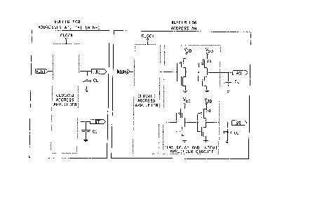
FIG. 1 is a schematic diagram of 2N decoder/driver
circuits according to the principles of the
present invention.
- FIG. 2 is a schematic diagram of N address buffer
circuits according to the principles of the
present invention~
FIGS. 3, 4, 5, 6 and 7 are illustrations of
waveforms of signals at various points in the
circuit shown in FIG. 1.
.
DESCRIPTION OF THE PREFERRED EMBODIiMENTS
A sch~matic diagram of 2N decoder/driver circuits
is shown in FIG. 1. Signal ~PC applied on
YO987-018
7~5~3
gate lead 13 of p-channel device 12 is a precharge
clock signal and signal ~R applied on gate lead 14
of n-channel device 1 is a reset clock signal. In
FIG. 1, a MOSFET device having a circle on the
gate lead, as shown in device 12, is a p-channel
device whereas a MOSFET without a circle on the
gate lead, as shown in device 1, is an n-channel
device. Devices 1,2,3,4 . . . 5,6,7 are connected
in a conventional OR decoder circuit
- 10 configuration, well known to those skilled in the
art. Lines A1 through AN are internal address
lines from the address buffers, shown in FIG. ~,
and the first Al-A~-1 address lines are connected
to the inputs of the OR decoder circuit in the
conventional manner. That is, the gate of each
device in the OR decoder circuit is connected to
either the true or complement address line for the
corresponding address bit from the address
decoders with the circuit drawn in FIG. 1 showing
the details of just one of the 2N OR decoders,
each of which is selected (low output) by a
different unique address while the remainder of
the OR decoders will be unselected (high output).
The true and complement lines or address bit AN
are both connected to the decoder/driver circuit
in the 1 of 2 selection stage, and are shown
explicitly in FIG. 1. The 1 of 2 selection stage
output is the input to the output drive~ stage~
The functional operation of the proposed circuit
will now be described. At the start of a cycle,
the address lines Al, Al, A2, A2, . . . AN, AN are
low as shown in FIGS. 4 and 5. The precharge
signal ~PC applied to the gate of p-channel device
12 on line 13 is low as shown in FIG. 3 and reset
Yog87-018 31~7:~559
signal ~R applied to line 14 is also low as shown
in FIG. 7. Node 16 is low and nodes 17 and 18
were discharged low when reset clock signal ~R on
line 14 went high at the end of the previous
cycle. At the beginning of the cycle, precharge
; clock signal ~PC goes high (see FIG. 3) turning
transistor 12 (Tl) off. It is assumed for
_ purposes of explanation that driver output WLi~1
is to be selected. For this case, address lines
Al,A2 ... AN remain low and Al,A2 ... AN go high.
Since all inputs to the OR remain low, node 16
remains low. Now as soon as signal AN goes high,
the node 18 is charged to VDD through transistors
11 and 20 (FIG. 2). As a result, the driver
output WLi+l is selected and goes high. All other
driver outputs including WLi remain low and thus
are deselected. If, on th~ other hand, signal AN
remains low and signal AN goes high, then node 17
is charged to VDD through transistors 9 and 19
(FIG. 2), selecting driver output WLI; all other
driver outputs remain deselected. If any one of
the address inputs Al through AN-l goes high, node
16 of the OR circuit will be charged to VDD,
turning off devices 9 and 11 and preventing the
charging of nodes 17 and 18, keeping both word
lines WLi and WLi+1 low or deselected regardless
of whether ~N or AN goes high. Thus, 2 N-l OR
circuits will have a node 16 that goes high and
only one of the 2N OR circuits will have a node 16
that is low, allowing a selected word line to rise
when either AN or AN goes high.
The decoding function of the circuit is summarized
in Table 1, where the state of the OR decoder node
16 will be low in precharge and remain low if the
YO987-018
~7~lS~
11
OR is selected; it goes high if the OR decoder is
deselected. If the OR is deselected (node 16
high), neither word line WLi or WLi+1 can be
selected, while if it is selected (node 16 low)
either WLi or WLi+1 will be selected, depending on
whether AN or AN goes high. Only one word line WI,
will be selected for a given address bit pattern.
TAsLE 1
OR DECODER
10 NODE 16 AN AN WLi WLi+1 CON~ITION
Low Low Low Low Low Precharge
Low Low High Low High Select WLi+1
Low High Low High Low Select WLi
High Low High Low Low Deselected
High High Low Low Low ~eselected
Towards the end of the cycle, the clock signal ~R
goes up and all address line signals Al through AN
as well as A1 through AN go low. The nodes 17 and
18 discharge low, pu}ling the selected driver
output low. At the end of the cycle, reset clock
signal ~R and precharge clock signal ~PC go down
as shown in FIGS. 3-7. As a result, node 16 is
pulled low, turning off devices 8 and 10, leaving
nodes 17 and 18 discharged low, but floating. To
avoid charging of the nodes 17 and 18 over a long
cycle time, an n-channel pull down device with
gate connected to VDD can be connected between the
node and ground. $his n-channel device should be
small compared to transistors 9 and 11 so as not
3~ to significantly 510w word line selection.
YO987-018
5~
It is necessary to have the internal address bit
signal AN/AN not arrive too early with respect to
the other address bit signals Al through AN-l. If
the address bit signal AN/~ arrives too early, it
can lead to an erroneous charging to VDD of nodes
17 and 18. For example, if node 16 will charge to
VDD when addresses Al through AN-l arrive, and if
line AN goes high before node 16 has charged to
VDD, then node 18 can at least partially charge up
towards VDD through devices 11 and 20 (FIG. 2) and
this can bring the associated word line WLi~l up
in error. This erroneous signal is transient, and
the circuit will eventually settle into the
correct output condition. On the other hand, it
is desirable to have the address signal AN or AN
arrive as early as possible to minimize delay
through the entire circuit. Thus, there is a
trade off in the early arrival of address bit
AN/AN between minimizing the delay through the
circuit and not causing an erroneous transient
charging. The circuit of this invention can be
readily optimized for minimum delay without
significan~ erroneous transient charging and
without substantial impact on overall performance.
Prevention of significant erroneous transient
charging is provided through two means; by delay-
ing the arrival of the address bit signal AN/AN
-with respect to the other address bit signals Al
through AN-l and through automatic additional
delay of the address bit signal AN/ AN when the OR
decoders are 510w in deselecting. The delay of
the address bit signal AN/AN is provided by adding
two pair of CMOS inverters to the outputs of an
address buffer of the same type as used for the
YO987-018
~7~
address bit signals Al through AN-1 as shown in
FIG. 2. Introduction of the delay of the address
bit signal AN/AN in this way places the same
number of n-channel and p-channel transistors in
the two circuit paths that control whether or not
erroneous transient charging occurs, the path from
the clock in`FIG. 2 to the output of the OR
decoders (node 16) and the path from the clock in
FIG. 2 to the address bit signal AN/AN. Thus, the
combination of the circuits in FIGS. 1 and 2
provides an easy means for equalizing the time at
which the 2N-1 OR decoders cleselect (node 16
rises) with the time at which the address bit
signal AN/AN rises. This provides the minimum
delay through the decoder/driver circuit without
causing an erroneous transient charging.
- Further prevention of significant erroneous
transient charging is provided by the interaction
of the decoder/driver circuits of FIG. 1 with the
~0 ~address buffers shown in FIG. 2 for the address
bit signal AN/AN. If the address bit signal AN/AN
arrives too early with respect to the other
address bit signals A1 through AN-l, then not all
of the 2N-1 OR decoders will be deselected and
address bit signal AN/AN will try to charge node
17 or 18 high in each of the OR decoders that have
not yet deselected. This increases the load
capacitance on the address line AN or ~ which
will slow down its charging to VDD through tran-
sistor l9 or 20 (FIG. 2). Thus, an automaticadditional delay of the address bit signal AN/AN
occurs when the OR decoders are slow in
deselecting. The circuits in FIG. 1 and 2 can be
readily optimized so that this additional delay
provides sufficient time for all of the 2N-l OR
;; ,;
YO987-018
715~39
14
decoders to deselect enough to prevent any
significant erroneous transient charging even in
the case where address bit signal AN/AN arrives as
early as the same time as the other address bit
signals Al through AN-l.
The circuit has a number of advantageous features.
There is only one OR circuit per pair of word
lines which helps to minimize the loading on
address lines. After the address lines switch, no
clocking is required before the selected word line
rises resulting in high performance. By applying
a rising signal to the source node of a p-channel
transistor in the 1 of 2 selection stage, two
stages of amplification can be used in the output
driver to charge a high capacitance word line to
VDD with minimum delay. If a more conventional
n-channel NOR/NAND decoder circuit were used, the
output driver could have only one, underpowered,
slower stage or three stages with greater total
delay. The use of source dotting on the address
lines AN,AN results in less delay in the 1 of 2
selection stage for a given capacitance load on
the address lines AN,AN as compared to a more
conventional n-channel NOR/NAND decoder circuit.
There is no dc power consumed, and dynamic charge
storage is required only for a short, well-defined
portion of the cycle.
It is understood by one skilled in the art that
the invention is not limited to the specific
embodiment shown. For example, the p-type and
n-type devices may be n-type and p-type
respectively, with corresponding changes in the
polarity of the signals and their complement.