Note: Descriptions are shown in the official language in which they were submitted.
4'7 11
The present invention relates to FM receivers and in
particular i9 directed to very qimple, compact FM receivers using two-
terminal negative admittance networks.
BACKGROUND OF THE INVENTION
In the conventional approach to FM receivers typically
one utilizes one separate electrical network for each function to be
performed such as amplification, frequency mixing, demodulation, etc.
- In the present invention, FM receivers include one or a small number of
electrical networks, such as two-terminal negative admittance networks
which perform multiple functions to form complete receivers. The
various functions performed simultaneously by the electrical networks
are primarily based on particular features of the non-linear negative
admittance of the two-terminal negative admittance network.
In another U.S. patent application No. 725,999
entitled "Two terminal negative admittance network" filed on April 22,
1985 by the inventor of the present application (now U.S. Patent No.
4,625,186 issued on 25 November 1986), a pair of active elements such
a3 transistor3 are employed in a novel circuit to form a negative
admittance network. Although the above patent is referred to in the
disclosure of the present application, it is felt that the present
invention would be more readily understood, if a brief description of
the two-terminal negative admittance networks is included in this
disclosure. The brief description will be found below.
Obiects of the Invention
It is therefore a principal object of the present
invention to provide compact and simple FM receivers utilizing negative
admittance networks.
It is another object of the present invention to
provide FM homodyne receivers which employ a negative admittance
netWork
It is a further object of the present invention to
provide FM superheterodyne receivers which use negative admittance
networks .
Summary of the Invention
Briefly stated, an FM homodyne receiver includes a
4~
--2--
two-terminal negative admittance network which has two terminals and
exhibits a negative admittance between them. The receiver further
contains resonance structure which is connected in series with the
negative admittance network. As readily understood by those skilled
in the art, the resonance structure can be made by a coil, a
transmission line structure or the like. Some preferred forms of the
resonance structure will be descrihed later in this application.
The resonance structure operates as an antenna to capture the RF
slgnal. A bipolar transistor is also provided at the point connecting
the negative admittance network and the coil, to produce the
frequency demodulated signal at its output.
In accordance with another embodiment of the present
invention1 a superheterodyne FM receiver is disclosed as containing
first and second two-terminal negative admittance networks, each
having first and second terminals and exhibiting a negative
admittance between the terminals. The receiver further includes a
resonance structure in which an RF signal i.9 induced and the
resonance structure is in series with the first negative admittance
network. A first transistor is connected to the point connecting the
coil and the first negative admittance network. Second transistor is
provided in series with the first bipolar transistor. The
superheterodyne receiver still includes a stage consisting of a
coil and a second negative admittance network connected in series
with each other. The output of the second transistor is connected to
the point connecting the coil and the second negative admittance
network to which point a third transistor is connected. The third
bipolar transistor produces a frequency demodulated signal at its
ouput. The receiver includes further a frequency feedback circuit
which feeds back the demodulated signal to the second transistor.
Brief description of the drawings
For a more complete understanding of the present
invention and for further objects and advantages thereof, references
may be made to the following description taken in conjunction with
the accompanyin~ drawings in which,
Figures 1 and 2 show two typlcal negative admittance
~7~
networks whtch can be used in the present invention and which are the
preferred embodiments for RF and IF frequencies respectively.
Figure 3(a), (b), (c) and (d) are curves showing thatthe
emitter resistance re and the base-emitter capacitance of a bipolar
transistor and the transconductance and gate-source capacitance
Cgs of a field-effect transistor are non-linear.
Figure 4 is a diagram of a FM homodyne receiver
according to the present invention.
Figures 5 (a), (b), (c) and (d) show schematlcally some
antenna tank "coils" which are used in the present invention.
Figures 6 (a), (b) and (c) show equivalent input
circuits of the radio receiver shown in Figure 4.
Figure 7 indicates the current-voltage behaviour Or
various parameters shown in figures 6(a), (b) and (c).
Figures 8 (a), (b) and (c) and 9 (a), (b) and (c) are
curves illustrating the behaviour of the oscillating tank circuit
during build-up period and equilibrium respectively.
Figures 10 and 11 are small signal equivalent circuits
of a homodyne receiver.
Figures 12 and 13 show graphs indicating relationships
of output signal amplitudes and frequencies under certain conditions.
Figure 14 shows graphically the operation of a
synchronous FM discriminator and limiter.
Figure 15 is a circuit diagram of a superheterodyne FM
receiver according to the present invention.
Figure 16 illustrates the linking of the two modules of
a superheterodyne FM receiver in both directionsJ by a coupling
transistor T2.
Figure 17 is a circuit diagram of the frequency
converter stage (module 1) of a superheterodyne FM receiver.
Figure 18 illustrates the action Or the external
frequency feedback loop of a superheterodyne receiver.
Brief description of two~terminal negative admittance networks
The admittance Y of the network shown in Figures 1 and
2, looking into the terminals 1 and 2 or terminals 3 and 4 is
Y = v = C + jB
where Y is complex having G (conductance) t})e real part and B
(susceptance) the imaginary part. '['he admittance is taken to be
negative when the real part C is negative. The input voltage is v
and the input current is 1 for both networks of the figures. The
admittance is non-linear when either G or B or both are a function of
the input current i or the input voltaKe v.
The negative real part, negatLve conductance G of the
admittance is crcased by various mechanism:
a) at low operating frequencles, a paral1el~voltage serie~-current
posltive feedback action creates a negative conductance C.
For medlum and high operating frequencies other rnechanisrns rapidly
overtake the feedback action, i.e.
b) the actlve devices, such as the transistors in the networks,
become increasingly cornple~ due to their small internal
capacitances and dynamLc impedances.
c) the lower effective impedance of Rs and Cs in parallel (shown in
Figures 1 and 2) towards higher frequencies.
d) transit diffusion delay across the base regions of the
transistors.
These effects (b), (c) and (d) are essential in
producing a negative conductance for higher operating frequencies.
I'he negative admittance is non-linear~ This is caused
primarily by the non-linearity in the emitter resistance re and the
base-ernitter capacitance Cbe of the bipolar transistors and the
non-linearity in the gate-source capacitance Cgs and the
tran3conductance of the field~effect transistors shown in Figures 3
(a), (b), (c) and (d). T~lese non linearitles are very essential in
the operations of the FM receivers.
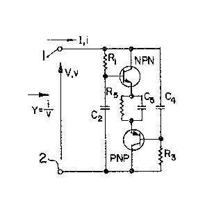
Detailed description of the FM homodyne receiver
.. ..
Referring to Figure 4, it is shown that a basic FM
homodyne receiver circuit uses a two~terminal negative admittance,
designated by a symbol indicated by Y. This symbol Y will be used
7~
throughout this specifLcation to show a two-terminal negative
admittance, sucl1 as those shown in Figures 1 and 2.
In Figure 4, the two~termina] negative admittance ls
connected in series with a coil 11 between the power supply 13 and
the groundplane 15. A bipolar tran.sistor 17 is connected at midpoint
and is fed by the power supply through a resistor 19. The transistor
17 produces a frequency demodulated output signal at the collector
21. The capacitor 23 together with resistor l9 forms a low~pass
filter, by-passing the l1igh frequency signal and satting the low
pass bandwldth of the demodulated output signal. The inter~electrode
capacitance Cbc f the bipolar transistor 17 is included in the
figure to show that the negative frequerlcy feedhack i3 beine
performed. The negative frequency feedback wilL be discussed later
ln this disc]osure.
The homodyne receiver shown in the figure performs,
unlike conventional receivers, all the functions needed for FM signal
reception such as functions of antenna, RF amplifier, local
oscillator, mixer, limiter, synchronous FM discriminator, automatic
frequency control and audio amplifier. It also includes a
frequency-feedback-loop via the base-collector capacitance of
transistor 17.
A detailed description Or these functions will be given
below under separate sub-headings.
Antenna
The receiver, as shown in Figure 4, uses only one
resonance circuit. It consists of an "external" inductor and the
"internal" capacitors, made up of the stray capacitances and the
small interelectrode ca~acitances of the bipolar junction transistor
17 and the susceptance part of the negative admittance.
The RF signal coil 11 forms the external inductor of the
resonance circuit and is optimized to be able to replace the function
of a conventional antenna. This optimization calls for minimum
capacitance in the tank circuit, therefore tunning capacitors are
eliminated. Moreover the susceptance part of the admittance is
minimized selecting high frequency transistors. For the same
resonance i`requency this allows one to increase considerably the
~ ~t7
-6--
inductance of the ~F signal coLl by increa31nK the number Or turns
and/or the diameter of the coil. ~his increase in number of turns
and/or diameter a1lows to capture much more ef`fectively the magnetic
field component and hence to become effectively an inductive antenna.
It wa~ found that mountine the coil over a groundplane further
increases its ability to operate as an antenna.
These "oversized" coils have wirelength which can be a
considerable portiorl of the wavelength. It is therefore more
appropriate to consider the coil a.9 a helix transnlission line mowlted
over a groundplane. For lower frequencies one can use ferrite rods
lnside the helix transmissioll line to maintain reasonable physical
dimen.sions. Various coils used are shown in Figures 5 (a), (b), (c)
and (d). In Flgure 5 (a) is shown a he]lx transmis3ion line 36
indicating a short helix transmission line over the groundplane 37
wLth the termlnals at one esld of t~le line and the groundplane.
Figures 5 (b) and (c) show flat coils etched in printed circuit
boards. The groundplane is desienated by 39 and 40 and the termlnals
are shown by dot;s at the ends of the coi]s. For very high
irequencies a new form of transmission line resonating structure has
been developed. As shown in Figure 5 (d), it consists of a closed
circular conductor mounted parallel to the groundplane 41 at a
height d, shown in tile figure, shorted at one point to the
groundplane. The terminals are taken at 43 opposite to the shorting
connection 45. This structure is particularly useful at frequencies
approaching I G~z where its physical size becomes very attractive.
Local oscillator
Conventional oscillators use positive feedback to create
and maintain oscillations in a re.sonance circuit. With a negative
admittance, however, simply shunting across a suitable resonance
circuit will generate and maintain oscillations if the power supplied
by the negative conductance of the admittance, at the resonance
frequency, is larger than the power dissipated in the resonance
circuit. The inherent non-linearities in the negative admittance
will result in a stable amplitude for the oscillations where power
delivered and power dissipated are exactly equal.
.
~L~7~
The operation of the osclllator is illustrated with
Figures 6 (a), (b), (c), 7, 8 (a), (b), (c) and 9 (a), (b), (c).
Figures 6 (a), (b) and (c) give the equivalent circuit diagrams. In
Figures 6 (a), U is a voltage generated across the coil whose
inductance is L and internal resi~tance is r. Ihe bipolar transistor
has the emitter resistance re and input interelectrode capacitance
Cbe between the base and emitter and CbC between the base and
collector. The negative admittance network is reduced to the
equivalent resistance Req and capacitance Ce~i. Figure 60 (b) is slmplified version of Figure 6 (a) using an equation
R = L
p rCT5
where CT = Cbe + CbC + Ceq and Rp Ls the equivalent
parallel loss-resistance of the coil.
Figure 6 (b) is ultimately sin~plified to Figure 6 (c)
where RT represents resultant resistance of Rp, re and Req
and the current is indicated by i.
Figure 7 shows the current~voltage behaviour of re,
RT, Rp and Req~ In the figure, i1, i2, i3 and i
represent the current flowing through Rp, re, Req and RT
respectively as indicated in Figures 6 (b) and (c).
The resistance RT, at i = 0 and u = 0 as shown in
Figure 7 is negative. Therefore the circuit will start oscillating
at the resonance frequency. The amplitude of oscillation will
continue to increase until some equilibrium is reached. The build-up
of the oscillation voltage and the stable equilibrium value reached
are illustrated in Figures 8 (a), (b), (c) and 9 (a), (b), (c). The
power dissipated in the resonance circuit over one cycle of
oscillation is expressed by:
7~L'7
P -- ~ 0 u(t) i (t) dt.
Ir P is positlve, then power is di.ssipated, whereas if P
i9 negative, power is supplied to the reqonance circult. In Figures
8 (a), (b), (c), P i~ negative hence power is supplied and the
ampLitude of the oscillation continue.~ to increase. In Figure~ 9
(a), (b), (c), the equi]ibrium situation is reached, i.e. P = 0, or
during one cycle, the power dissipated is exactly equal to the power
delivered by the negative resi~tance. Craphically this means that
the positive and negative surface areas have become equal.
RF amplifier, synchronous FM discriminator and limiter
Ihe RF signal is captured by a tank circuit which i8
oscilLatlng at its resonance frequency. It will be ~hown how, when
the RF and the L0-frequencies are very close, synchronizatlon of the
two signals occur.
Furthermore it will be shown how, effectively,
amplificatlon Or the RF signal is obtained. Moreover that, for
certain conditions, the frequency modulation of the RF-signal not
only results in a frequency modulation of the local oscillator due to
synchronization, but also in a linear transfer of the frequency
modulation Or the RF-signal to amplitude modulation of the oscillator
signal, hence frequency discriminator action.
Also, the FM-to-AM conversion will be shown to be
independent of the amplitude of the RF signal, therefore the
equivalent action of a limiter is performed.
Therefore the analysis below will show how the
equivalent functions of RF-amplifier, limiter and synchronous
FM-discriminator are obtained. First some basic relation~ will be
derived to be applied subsequently to analyze the RF-amplification
and the synchronous FM discriminator/limiter action.
Referring back to figure~ 4 and 6 (a), (b), (c) where
the receiver circuit and its equivalent are shown.
~7~ 7
If t~e effective conductance in parallel wlth the
inductance 1. is negative, osci]lations will result. The frequency ls
determined by the value of L and the total equivalent circuit
capacitance Cl in parallel with the inductance L. The amplitude of
5 the oscillation is stabilized by the non~linear behaviour of the
conductance. Both the conductance part of the negative admittance Y
and that of the transistor 17 are non~linear. The non~linearity of
the transistor 17, however, becomes dominant, when the signal exceeds
the base~emitter threshoLcl.
Trans1stor 17 is confL~;ured a.<~ a C-class amplifier.
For small amplitude osclllation, the transl3tor 17 does therefore not
load the resonance circult. Iï the ampl ltude of oscillation
increase.q and exceeds the base-emLtter threshold voltage, then the
transistor starts drawing current durLng the posltive peak3 of the
15 oscillator signal. The loaAing by tran3istor 17 increa3es very
rapldly, therefore the amplitu(le of oscillation stabilL3e3 at the
onset of the threshold voltase, about 0.65 volts.
As seen in figure 5(a), the capacitance of the resonance
circuit consi3ts of the equivalent capacitance Ceq and
20 interelectrode capacitances Cbe and Cbc of the transistor 17.
These capacitances are voltage dependent and hence non-linear.
Now let us consider a small signal with a frequency
equal or very close to the resonance frequency, being introduced into
the oscillating network either by injection from a current source or
25 induced by flux linkage from a remote transrnitter. Both cases are
equivalent to a small voltage source Ein put in series with the
coil as shown in Figure 10. In the figure, the resonant voltage U,
current I and induced signal voltage Ein are shown. It is assumed
that ¦Ein¦¦U¦. The current I through the inductor L can then
30 be considered constant and independent of the voltage source Ein.
Thi3 assumption allows us to replace the voltage source Ein by a
small fictitious complex impedance z which will be given by
35 z = ~r + j~o~L =
:
- l o -
using small disturbances ~L and ~r of inductance L and resistance r
respectlvely. If z is chosen equal to
E.
ln
z
then Figures 10 and 11 are equivalent. The equivalent model of
Figure 11 permits us to analyze the relationship between both
frequency and amplitude of the oscillation as a function of the
induced voltage in terms of a small disturbance of the inductance L
by a small impedance z.
In Figure 11, the following symbols are used:
15I = Ie~
20Ein E e i(~It + ~)
lJ
30 z s ~r + J~0 ~L ~ I
where
~l - frequency of induced signal Ein
= undisturbed resonance frequency of oscillator
= instantaneou~ frequency of oscillator
) s dif~erence in frequency between Ein and
undisturbed frequency of osolllator
(~0 - ~0) = change in oscillator frequency due to induce signal
) = instantaneous beat frequency between oscLllator and
in~ected signal
= instantaneous phase angle between current I and voltage
Ein ~
The differential equation relating Ein and I is
dt (~ o)
.
: ~
.
~. .
:: . : ,
., . ~ ,
d(~/dt represerlts the instantaneous heat t'requency. To slmplif'y the
analysis lt Ls assumed that synchronlz;ltion between induced signal
Ein and 030111ator signa]. U has occured. Theref'ore
d~ = 0
1 !~
hence ~ = constant and w~ = wO .
The frequency ~0 and the amplltude U of oscill.atlon are
non-linear runctions of r and L. For srna.L:L variatlon.q arouncl
operatlng polnt wO and U0, one can linearize these relatLons usLng
expansion in 'I'aylor serles for a function of two variables ancl
retaining only the first order terms.
U = U0+~r aU + ~0 AL ~0 aLI
25 wO = ~0 + ~r aW + ~o~LIl aL (2)
~ 30 Let us consi.der now
au d 1 au
a ~OaL
as the components of a vector A at angle a and aar and - ~Q
as the components Or a vector F at angle ~.
then
~ aU = A cos~ 1 aU = A sill~
~ = F cos~ ~0 aL = F sin~
~27~7
~12~
Meanwhile, the fictitious impedance z is defined as
z = ~n = ln ej(~t~~Ot + ~)
where ~ is a phase angle between Ein and I.
10 Signals are synchronized, hence ~ 0, thus
_ Ein ei~ = (Iln cos ~ + i ( I
Because z = ar + j~o~L~ it follows:
~r = ln
AL Ein
Consequently equations (1) and (2) can be rewrltten lnto:
(U - U0 ) = in A cos (~ ~ ~) (3)
(~0 _ ~o) = in F cos (~~3)
I
Relationships (3) and (4) will be used to analyze the functions of
"RF~amplifier" and "Synchronous FM discriminator".
RF-amplifier
The RF signal is induced into a circuit which is
: oscillating at the frequency o~ the RF-signal (signals are
; synchronized). The RF gain i9 defined as the change, au = Uo-U7 inthe amplitude brought about by the induced RF-signal, Ein.
~: :
~'`
. . . .
. :
.
,
From equatLon (3) above, the I~F-gain Is expressed,
F~F-gain U ~ UO = A cos (~
Optimum RF gain is obtained for minimum I and maximum A.
Various ways of optimizing RF gain are discussed below:
"I" It is obviou.s that I can be reduced by decrea~ing U, the
amplitude of oscilLation, since I is directly proportional to U.
The current I is also reduced by decreasing CT as much as is
possible, allowing the inductance 1. to increase, keeping the
resonance frequency constant. The impedance ~oL is hence
maxlmum and for a given U, minimum current I flows through the
inductance L.
"A" Vector A is composed of two components ar and ~ aL then
A is:
A = {(aU)2 ~ (1 aU )2~1~
To minimize I, L is maximized, therefore minimizing - aaL I~ence
to maximize A one ls left with aL ~ which should be made as large as
possible. This is obtained by striving for the oscillation to be
very marginal. i.e. keeping the non-linearity in the negative
conductance 1/Req as small and smooth as possible. Any resistive
disturbances ~r, will then result in a large shift in the amplitude
of the oscillation. This can be seen readily from an inspection of
Figures 7, 9 (a), (b), (c).
Making 1 aU very small and aU very large yields for :
t~ = ( l au ~ 3U ) O
therefore = ~O With ~ = ~, it follows that cos (~
cos ( ~-lr )= - cos ~ .
., 11_
T~le RF gain, and hence the sensititivy, of the recelver
i8 thus optimlzed with L large, Ceq and U small and f`urthermore
keeping the oscl]lator very marginal, i.e. reducing the non~lLnearity
ln the negative admittance to a minimum.
Synchronous F'M discriminator/limiter
Three basic requirements are implicit in the operatlon
of a limiter and a synchronous YM Aiscriminator:
1) Limiter keeps the output signal constant independent of the
induced RF signal.
2) Synchroni%ation between ~F signal an(l local oscillator signa].
3) ~inear conversion from FM to AM modulatlon.
The synchrorlizatioll has been analyzed above and resulted
in relatlonship expressed by equation (Il). The maximum values for
cos (~ ) are ~1. The maximum range over which syrlchronization can
take place .i9 tilerefore
~ 1n F (}I )
Notice from the expression above that thi~ range is directly
proportional to the amplitude Ein, of the induced RF signal and
inversely proportional to the current, I, and hence U, the amplitude
of the oscillation.
To analyze the limiter action and the linear conver~ion
of FM and AM modulation we will need both relationships (3) and (4).
Eliminating ~ from these equations gives the relationship
cog l{(~o-~o) -E F ~ ~ cos '{(U-UO) E A ~ ) (5)
One can see from the above equation that the change in amplitude of
the o~cillator, (U-UO), is an implicit non~linear function of both
the input frequency change, (~ O) = (~0- ~0) and the amplitude,
Ein, of the induced signal. Hence, the two basic requirements
for a FM discriminator/limiter, i.e. linear FM to AM conversion and
conversion independent of input amplitude, are not satisfied, in
; general. There are however two specific values for (~-~), for which
the above requirements are met and they are (~-~) = O and (~
rad. In these cases equation (5) above becomes:
t;~t~7
~15-
A
U-IJ0 = F (~ O) when (a~~) = 0
U-U0 = F (mO ~ mO) when (~ rad.
These relations aie shown in Figures 12 and 13.
It is shown previously that = ~. Hence ]inear
conversion from FM to AM rnodulatLon 1s obtalned for ~ = 0 or e = Ir.
To show how this condition can be attained we have to look at
relationships derived above:
a~Q = F cos ~ 1 a~Q_ - F sin
ar (J al,
Combining the above equations glves
tg~ _ 1 a Q/ Q
3o
Imposing ~ = 0, ~ requires that
~0 aL ~Q (6)
(For conventiona:L feedback type of oscillators the above
condition (6) is not satisfied, in effect the opposite is true.) As
explained earlier, the oscillator is very marglnal i.e. aU~ar is very
large, hence any change Qr results in a large variation in U.
With CT (Figure 6 (c)) being voltage dependent, a
large variation in U leads to a corresponding large change in the
resonance frequency ~0 (Cbc o~ transistor 17 also plays an
important role as will be described under "frequency-feedback-loop't).
Effectively one has a~0/ar very large and positive
compared to liwo-a~t/aL~ which is small and negative.
Therei`ore the angle ~ is very small. With ~ = 0 and
= ~r it f`ollows that (~
Thus equation (5) can be simplified to:
(U-U0) = ~ F (~ ~ ~) (7)
~'7
- 1 6--
Several irnportant f'eatures f'ollow from relatlon (7)
above.
1) Relation (7) shows clearly that a change in frequency is
converted linearly into a corresporlding amplitude change, hence a
llnear conversion from FM to AM modulation.
2) The conversion gain factor A/F, is only a function of circuit
parameters, independent therefore of the amplitude of both the
injected signal and the oscLllator signal. Therefore one has the
equivalent of a limiter, hence AM reJection.
Relation (7) is shown gr-aphically in Figure l4. Whereas
the conversion gain A/F and hence the slope in Figure l3 is
independent of both the amplitude Eir~ of induced RF signal and
the amplituds of osclllation, one notices, as shown, that the range
of synchronization depends both on the amplltude of induced signal
~in and the amplitude U = (I~oL), of oscil'Lation.
The RF and local oscillator frequencles synchronize
; inside the synchronlzation range. The function of automatic
frequency control of conventional FM receivers is therefore performed
automatically.
Mixer
The function of a mixer, in a receiver, is to
; down-convert the frequency of the RF-signal to a more convenient
lower level, as is commonly done in superheterodyne receivers.
In a homodyne type receiver, however, the RF signal has
the same frequency as the local oscillator and therefore the beat
signal is at DC. The basic requirement of a mixer is to have a
non-linear behaviour so as to be able to produce the beat frequency.
In the two-terminal negative admittance homodyne receiver as shown in
Figure 4, this non-linear behaviour is provided by the two-terminal
negative admittance itself as well as by the non-linear loading of
translstor 17 of the resonant tank circuit.
Demodulator/audio amplifier
As was explained above in connection with RF amplifier
and synchronous FM discriminator/limiter, there is a linear
conversion obtained from the FM modulation of the input RF-signal to
AM modulation of the local oscillator signal. The AM modulation
'.',;:.. .. .
.:^.:..,...,,;.: ..
' ' ' ` ,::
3 ' "7~ " ~
~17~
of the local oscillator slgna] however has to be demodulated to
obtain a base-band output slgnal. The demodulation, audio
amplification and low pass filtering are performed by transistor 17
shown in Figure ll. The transistor 17 has no DC pre--bias. The
positive peaks of the oscillating slgnal forward bias the transistor
producing current pulses into the base. They are amplified by the
transistor and smoothed by the RC low-pass net~lork. The base band
output signal is available at the collector of the translstor.
Frequency - feedback - loop
Referring back to Figure ll, transistor 17, p]ays an
important role in a frequency-feedback-loop, vLa the base~collector
Jurlction capacltor Cbc.
We assume t!lat the negatLve admLttance circuLt has
synchronized ~ith the induced RF-signal, hence ~, = oO.
A change Ln the frequerlcy ~1 of the induced RF-signal,
results ln a corresponding linear change in the osclllator signal U,
as explained earller.
This amplitude change is amplified, rectified and
averaged by the transistor 17 - operating in c:Lass-C mode- and
re~ults in a DC-signal on the collector.
The base-collector capacitance Cbc is voltage
dependent and therefore directly influenced by the voltage on the
collector.
Varying the magnitude of CbC changes the resonance
frequency wO of the tank circuit.
There is thus a frequency-feedback-loop: a change in the
frequency ~, of the RF-signal is sensed by the negative admittance
network and results in a change in the resonance frequency, ~0, of
the tank circuit.
This external frequency tracking reduces the lock-in
effort imposed on the negative admittance circuit to keep the
induced RF-signal (~,) and oscillator signal (~0) synchroni~ed,
resulting in an extended synchronization range.
Superheterodyne FM-receiver and Frequency-converter
The sensitivity of the homodyne receiver can be
substantially improved by using negative admittance circuits to
' ~ ,
~18-
implement a superheterodyne type of' F'M receiver.
This permits signal amplification of the signal at the
intermediate frequency before it is presented to the homodyne
receiving stage, which is now operating at this intermediate
frequency.
The circuit diagram of the negative admittance
superheterodyne receiver i9 shown in Figure 15. It can be separated
into two functional modules which are linked together by transistor
T2, as schematically shown in Figure 16.
The functions performecl by these two modules are:
Module 1: Antenna, RF amplifier, ~F local osci11ator, RF mixer and
IF amplifier
Module 2: IF local oscillator, IF mixer, Synchronous Frequency
discriminator with AM-reJection and Audio amplifier
Module 1 and 2 are further linked by a:
Frequency-Feedback-loop.
Note that f'or the analysis of the IF-amplifier one has
to consider both module 1 and module 2, due to the close integration
of these modules.
Module 2 operates as the homodyne FM receiver, however
it now operates on the IF beat frequency produced by module 1.
The operation of the homodyne FM receiver has been
described in detail above; we retain here only that it synchronises
with the IF signal and that it produces a linear conYersiOn from
frequency to amplitude modulation.
~ he f'unctions of module 1 - also referred to as
frequency converter ~ such as antenna, oscillator and mixer are
essentially as described for the homodyne receiver. Wit~l regard to
the mixer, the difference however is that the beat frequency is not
taken at zero Hz but at a certain IF frequency.
A new function is that of the IF-amplifier. Also there
is an outer frequency feedback loop which results in a substantial
compression of the signal bandwith. These two functions will be
described next.
IF-amplifier
The circuit elements constituting the IF-amplifier are
'" ~'~ .
, 9~
shown in F`igure 17. Tran3lstor Tl ha3 no l)C-preblas. The posltl~/e
peaks of the RF local 03clllator signal jllSt; exceed the base-emitter
~unction threshold of transistor T" producing current pulses in the
transistor. These current pulses contain the IF beat sienal which
are amplifled by transistor T, to produce an IF voltage ~ignal
across the IF tank circuit made up an inductance L2 and total
inherent clrcuit capacitance C2. Capacitor Cl by passes the RF
signal at the collector of transistor Tl. rransistor T2 decouples
the IF signal from transistor Tl, allowing a larger IF gain to be
obtained without oscilLatLng instabilities. Transistor T2 also
complete~ the freqllency-~eedback-loop, described next.
F quency-FePdback-loop
The homodyne stage of the superheterodyne receiver has
lts local frequency-feedback loop. This functions as described for
the homodyne receiver.
There is another frequency-feedback-loop, an outer loop
from output to input module, as indicated schematically in Figures 16
and 18.
In conventional superheterodyne FM receivers there is
some limited fcrm of feedback which iB restricted to DC operation
and is referred to as automatic-frequency-control (AFC). Its role is
to stabilize the frequency of the local oscillator. In the present
embodiment the feedback is dynamic, i.e. all of a the signal output
frequencies are fed back to the input, including the DC components.
The transistor T2 (Figure 16) is an essential "pivot
point" between the two stages of the receiver, handling
simultaneously and independently the information flow between these
two sta~es. In the forward direction, transistor T2 transmits the IF
signal to the following stage and at the same time decouples the
amplified IF signal from the input stage. In the reverse direction,
transistor T2 takes the demodulated FM output signal and feeds it
back to the input stage where it controls the frequency RF local
oscillator. Transistor T2 operates as an unity gain voltage
follower imposing the output signal on the collector o~ transistor
T, and therefore controlling, via the voltage dependent base
collector junction capacitance Cbc of transistor Tl, the
. ,.
.
'7~
20--
frequency of the RF osolLlator.
The essent~al operations of the FM receiver wlth regard
to frequency feedback are il]ustrated in Figure 18. The basic action
of module 1 i3 to down convert the RF frequency to an intermediate
frequency. Module 2 can i1ere by simply consldered as a
frequency-to~voltage converter. Its output, via the feedback loop,
controls the frequency of the RF-osclllator.
~ he first consequence is that the local oscillator
frequerlcy is slaved at a constant offset (LF frequency) to the
RF-frequency. This is comparable to conventional automatic frequency
control.
However all baseband signal frequencles are fed baok.
Thls has an lmportant effect on the 3lgnal bandwidth.
Indlcating variations ln the frequencles by the symbol
f, the following relations follow from inspectlon of Figure 18.
if rf fLo
V0 = ~ ~if
fLo = B V0
where V0 is the output voltage and and ~ are conversion gain
factors of module 1 and module 2.
Combining these relations, one can readily derive for
the overall frequency-to voltage conversion,
3o
VO
frf 1 ~ ~
and for the frequency deviation compression ratio:
rf = 1 +
if
.:..
~7;~ 7
21-
Assulning some typlcal. values ~or ~ and ~, 1 volt/k}lz and
1 MHz/volt respectively one obtains,
. = 1 volt/M}Iz and i~f 1000
frf ~if
Consequently a 100 kHz deviation of the RF frequencies
produces only a 100 Hz deviation of the IF f'requency and an output
voltage change of 100 mV.
It is obvious therefore that, contrary to conventlonal
FM receivers, a substantial signal bandw.i.dth compression takes p],ace
from RF to IF. The IF stage has to pass only the mo~ulatlon
frequencies and not the large associated frequer1cy deviations
inherent in the frequency modulation process.
3o