Note: Descriptions are shown in the official language in which they were submitted.
~ ~J'7~
UNI~ERSAL MODULE INTERFACE
Background of the Invention
This invention relates to modular electronic
systems, and more particularly to an interface
circuit facilitating automatic determination of
module presence and conf iguration.
As technology ~dvances in the fields of data
store, integrated cixcuits, circuit packaging and
interconnection, available modules tend to change
in size and storage capacity. For exa~ple, a new
module of given size may be provided with increased
data-store capacity, or a new version of a module
storing a fix~d amount of data may become smaller
in physical size.
In the past, new technology modules such as
data-store modules were often incompatible with
existing equipment. Replacement of defective
modules in existing equipment with new-technology
modules was often impractical or impossible because
of the need to change either the arrangement of
inter~ace signal connection~, or the mounting
hardware, to accommodate the new module.
Accordin~ly, it is an object of the invention
to provide, in a modular electronic system, an
improved interface between the system and modules
connec;able to the system.
It is another object of the invention to pro~
vide an improved dual-function interface-signal
circuit.
Another object of the invention is to provide
improved apparatus for automatically determining
the size and configuration of connectable modules
such as data-store modules in a modular electronic
system.
.,, , ~ :-
. ,.,:~
r~, ~
The present invention provides a universal moduleinterface circuit wherein a control unit of a central
system communicates interactively via one or more
control signal interface leads with a connectable module
of the system to determine the configuration of the
module, and generates module control signals
corresponding with the configuration determined. The
module includes a control signal generating element that
impresses on the interface lead a signal representing a
physical configuration such as data-store size of the
module. The control signal interface leads are
conventionally used for transmitting control signals
from the control unit to the module; however, to
determine module configuration, the control unit
disables normal generation a control signal on an
interface lead, and enables reading of the module
configuration signal on that lead. The control unit
stores and subsequently utilizes the module
configuration siynal to generate a module control signal
that is impressed on the interface lead for transmission
to the module.
In accordance with one aspect of the invention
there is provided in a modular electronic system, a
universal module interface, comprising: a control unit;
a modular unit connectable to said control unit and
receiving control signals from said control unit when
connected thereto, said connectable modular unit being
capahle of more than one system configuration; means for
transmitting a control signal between said control unit
and said modular unit; means in said modular unit ~or
generating a configuration control signal representing a
system configuration of said modular unit; means in said
control unit for receiving said configuration control
signal via said control signal transmitting means during
a first time period; means in said control unit havlng
an output coupled to said control signal transmitting
means and responsive to said configuration control
signal for generating a module control signal; and means
in said modular unit ~or receiving said module control
signal via said control signal transmitting means during
: ' '
~'7~
2a
a second time period.
Brief Description of the Drawin~
While the invention is set forth with particularity
in the appended claims, other objects, features, the
organization and method of operation of the invention
will become more apparent and the invention will best be
understood by referring to the following detailed
description in conjunction with the accompanying
drawings in which:
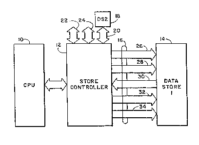
FIG. 1 is a block diagram of a modular electronic
system in which the present invention is utilized;
.: :,
;
9 t;~ r
-L~ ~3
FIG. 2 is a schematic block diagram of one
embodiment of the instant invention; and
FIG. 3 is a schematic diagram of ~ circuit in
accordance with the invention.
Descri tion of the Preferred Embodiment
P ~ . .
Refexring now to the drawings for a more
detailed description of the construction, operation
and other features of the instant invention by
characters of reference, FIG. 1 shows a modular
computer system comprising a central pxocessing
unit (CPU) 10, a store controller 12 and a data
store module 14. The data store module 14 is
connected to the store controller 12 by way an
s interface or input/output port 16. A second data
store module 18 is connected to the store control-
ler 12 by another port ~0 while addi~ional data
store modules (not ~hown) may be connected to
vacant interface ports 22, 24 of the store control-
ler 12.
The interface ports 16, 2n, 22, 24 are eachcomprised of a plurality of signal leads or buses
that form an interface between the store controller
12 and the data store modules connected in the
system. The inter~ace 16 typically includes a
multiplexed address bus 26, a data-in bus 28, a
data~out bus 30, a timing signal bus 32, and a
module and bank select bus 34. The functions of the
various interface buses and lines are conventional
and well Xnown in the art.
The data store of FIG. 1 repre~ents the main
internal ~tore of the computer sy~tem of the
presently described embodiment of the inventl~n.
Such data store may be made from either semi~onduc-
tor devices ox magnetio core modules having ~ycle
times ranging rom 20 to 2000 nano~econds. Datastore is divided logically into separately addres-
sable groups termed herein "fields", and physically
divided into groups called "banks". A logically
addressable field of data store may be physically
lccated in more than one data store bank. A
"module" means a physical arrangement of one or
more banks of data store on a connectable as~embly,
alternatively called a "card" or a "board". Modu-
lar arrangement of the data store may facilitateinternal time-sa~ing operations of the system such
as overlapping and interleaving of the data store.
In the presently described embodiment of the inven-
tion, sufficient address lines are provided in the
interface to address modules having one megabit of
data store. In addition to addxess lines, four
bank select signals, e.g. CAS0-CAS3, and two
module select signals, e.g. CARD0, CARDl, may be
provided on buses such as bus 34. Each of the
modules 14, 18 suitably includes four banks of data
store, each bank having 0.25 million word ~ The
system of FIG. 1, utilizing the two modules 14, 18,
is thus capable of addressing two million words of
data store. If the modules 14, 18 were eaoh
capable of holding, SAy, only two banks of data
store because of physical size limitations imposed
by bit density of the particular technology
~mployed to manufacture the data store ~odules,
then four modules would be rPquired to achieve th~
same two million woxd data store capacity. The
store controller 12 according to the present inven-
tion senses the presence of and determines the siz~
and configuration of each data store module connec-
ted in the system?
Referring to FIG~ 2, an interface circult in
,- ~ ,
,
,.
~7~'7~ S ~ ~
accordance with the present invention includes a
typical m~dule interface lead 40 havin~ a first
portion 40' thereof in the store controller 12 and
a second portion 40" in the data store module 14,
the line ~0 being connected at an interface connec-
tor represented by a dashed line 42. A program-
mable logic array (PLA) 44 receives a control sig-
nal CS2, which may be a data store address signal
or other control signal, for transmission from the
store controller to the data store module 14. A
tri-state logic element or gate 46 of the logic
array 44 receives the CS2 control signal and
regenerates it at an output node 47 under control
of another control signal CSl. The CSl control
si~nal is in a first logic state during a first
time period, and in a second logic state during a
second time period. During the second time period,
the tri-state gate 46 is selected or rendered
active by the CSl control signal on input connec-
tion 48, and the gate 46 will transfer a logical 0
or logical l state of the CS2 si~nal to t-he output
node 47 which is connected to the interface lead
40'. The data store module 14 then receives the
CS2 control signal by way of a gate 50 connected to
the interface lead 40". During the first time
period, the CSl signal disables ~he tri-state gate
46, and the tri-state output appears as an open
circuit of very hi~h impedance at the output node
47. Information in the form of a plurality of
discrete data items representing the confiyuration
of the data store module 14, e.g., the size of the
data store, the number of data store banks on the
module, etc., can be communicated at such time to
the store controller 12 via the control signal
interface leads such as lead 40. For instance, a
:
; ~
. . ,, ~,:
: ', ':
resistor 52 connected in the module 14 from the
interface lead 40" to a positiv~ power source 54
can genera~e a logic 1 data item on the interface
lead 40" while absence of the resistor 52 can
generate a logic 0 on the lead 40".
A logic gate 56 of the PLA 44 is connected to
the interface lead 40', and regenerates the data
item received from the module 14 as a configuration
control signal CS3. A latch circuit 58, which may
be for example an RS bistable, stores the CS3
contrc~l signal in response to the first logic state
of the CSl control signal connected via lead 60 to
an enabling input of the latch circuit 58.
A logic element 64 of PLA 44 is also enabled
by the CSl control signal during the second time
period to provide a regenerated control signal CSNl
for operating the data store module 14. The CS~l
control signal, which may, for example, be a module
select or a bank select signal, is transmitted to
the data store module 14 on interface lead 66. The
CSNl control signal is suitably a logical combina-
tion of control si~nal CSN generated in ~he store
controller and configuration control signal CS3
from the module 14.
A pull down resistor 70 serves to generate a
logic 0 on the interface lead 40' when the resistor
52 is not connected in the module 14, or when ~he
data store module 14 i5 removed from the system.
Means are thus provided which can be used for
detecting physical presence of a ~odule cvnnected
to the interface connector 42.
Ref~rring the FIG. 3, a detailed illustrative
embodiment of the present invention include~ a
programmed logic array 80 receiving address signals
R18-R22, A20-A23: and control signals RST, RFCYCLE
r~
and RFSCRUB from the store controller, and config-
uration control signals CARD0, CARDl, and 4MSIZE
from the data store module. The address signals
A20-A23 represent data store address bits for
normal data store access while the R18-R22 address
signals represent data store address bits for
address generation during a data refresh cycle.
The RFCYCLE and RFSCRUB signals are utilized for
refresh address generation. The RST signal is a
configuration control signal generated in the store
controller, and corresponds to the CSl control
signal of FIG. 2. The CARD0 and CARDl signals are
~odule-select control signals generated by the PLA
80 during the second time period of the configura-
tion control signal (/RST), while the signals CARD0
and CARDl also represent conficuration data items
input to the PLA 80 from the data store module
during the first time period of the configuration
control signal (RST). Bank select signals CAS0-
CAS3 ara logically dexived in the PLA 80 from the
input address and eontro~ signals as shown below i~
logic equations. The CAS0-CAS3 bank select signals
are stored in latch circuit 82 (corresponding to
latch 58 in FIG. 2), respectively as card count
signals MC0 and MCl, card present signal CARDS, and
data store size signal 4MSIZE. The PLA 80
generates the data store control sisnals in accor-
dance with logic equations programmed into the PLA.
The logic structure of the output signa1s is dis-
closed below in the form of Boolean logic equa- -
tions. In the equations, a "+" symbol or logic
operator denotes an OR function, and ~ "*" symbol
indicates an AND function. A "/" symbol prefix of
a log~c na~e means that the signal is the comple-
ment of the named signal (positive logic is uti-
.: ":
''~' ' ' ' , , .
, : '.~''', :, ''
~ .. ..
t~;~rj i
lized), i.e., "/" means that the voltage level
associated with the term is the less positive
leYel, and the term is enabled or high w~en that
level is present ~n the signal node. For example,
the CAS0 signal is enabled when th~ /CAS0 signal
node is at the less positive level, and disabled
when the /CAS0 node is at the more positiv~ level.
A logic term without a suf f ix symbol indicates that
the voltage level associated with the ter~ is the
~ore po~itive level and the term is enabled ~r high
when that level is present on the signal node~ An
"If" logic operator precedes a tri-state gate con-
trol signal such as the signal RST. Th~ PLA 80 of
the present invention is a Model 20L8A pr~grammable
array logic circuit manufactured by Monolithic
Memories Inc.
If /RST /CARD0 = (/RFCYCLE * /4MSIZE * /A21 * /~20 * ,/A23)
~ (/RFCYCLE * /4MSIZE * /A21 * /A20 * ,/A22)
2Q + (/RFCYCLE * 4MSIZE * /A22)
+ (RFCYCLE * RFSCRUB * /4MSIZE * /R21 I /R20)
~ ~RFCYCLE * RFSCRUB * 4MSIZE * /R223
If /RST /CARDl = ~/RFCYCLE * /4MSIZE * /A21 * A20 * /.A23)
~ (/RFCYCLE * /4MSIZE * /A21 ~ A20 * /A22
+ ~/RFCYCLE * 4MSIZE * A22 * /A23)
+ (RFCYCLE ~ RFSCRUB * /4MSIZE * /R21 * R203
+ (RFCYCLE * RFSCRUB * 4MSIZE * R22)
/CAS0 = (/RST * /RFCYCLE * /A23~
~ (/RST * /RFCYCLE * /A22)
3~ + (/RST * RFCYCLE * /4MSIZE * /R19 * /R18)
(/RST * RFCYCLE * 4MSIZE * /R21 * /R20)
+ (RST * /CARDl)
CASl = (/RST * /RFCYCLE * /A23)
+.~/RST * !RFCYCLE * /A22
+ (/RST * RFCYCLE * /4MSIZE * /Rl9 * R18
,
r~~
.~3
t/RST * ~FCYCLE * 4MSIZE * /R21 * R20)
+ RST
/CAS2 = (tRST * /RFCYCLE * /A233
+ ~/RST * /RFCYCLE * /A22)
+ (/RST * RFCYCLE * /4MSIZE * Rl9 * /R18)
~ ~/RST * RFCYCLE * 4MSIZE * R21 * /R20)
+ (RST * /CARD0 * /CARDl)
If /RST /CAS3 = (/RST * /~FCYCLE * /A23j
~ (/RST * /RFCYCLE * /A22)
~ ~/RST * RFCYCLE * /4MSIæE * Rl9 * R18)
~ ~/RST * RFCYCLE * 4MSIZE * R21 * R20)
While the pr:inciples of the invention are
evident from in t'ne foregoing illustrative eMbodi-
ment, there will be immediately obvious to those
skilled in the art many modifications of structure,
arrangement, and components used in the practice of
the invention, and otherwise, which are particular-
ly adapted for specific environments and operating
requirements without departing from those princi-
ples. The appended claims are, therefore, intended
to cover and embrace any such modifications, within
the limits only o~ the true spirit and scope of th~
invention.
~, .
:
- - ; . ~ . . ~ . . ...
. . :: , ,. :
:
.,, .,
-: : ,. :: : .
:
. ~. , . , :