Note: Descriptions are shown in the official language in which they were submitted.
5~
-- 1 --
SE~MICONDUCTOR DEVICE INCLI~DII`IG AN EPITAXIAL LAYER
ON A LATTICE-MISMATCHED SI~IGLE CRYSTAL SUBSTRATE
Background of the Invention
This invention relates to semiconductor
devices including contiguous layers of lattice-
nlsmatched materials.
In a variety oF electronic circuit contexts,
it is desirable to have available epitaxial layers of
lattice-mismatched materials, each of the different
mate~ials being used to provide a device function which
is ~est accomplished using that particular material.
~lowever, because of the lattice mismatch between
different semiconductor materials--e.g., about 0.22
Angstrom or about 4% mismatch between Ge and Si--during
lS epitaxial growth, great stresses are unavoidably
established in the region of the interface of epitaxial
layer and substrate, whereby the epitaxial layer suffers
in quality from such defects as lattice dislocations, so
that transistors formed in the epitaxial layer ~o not
operate properly, if at all. As the epitaxial layer is
made t~icker, the formation of lattice dislocation
becomes more likely. For example, in order to ~row upon
a sincJle crystal silicon substrate a dislocation-free
epitaxial layer of Gex Sil x having a thickness of even
2S as little as 100 Angstrom, the Ge content must be
limited to a mole fraction x less -than about 0.5,
whereas a mole fraction x equal to unity (pure Ge~ is
desirable for optical elements formed in the epitaxial
layer, and in prior art such a layer (with x=l) cannot
be grown dislocation-free upon a silicon substrate
regardless of how small the thickness of the layer is
made. More generally, it is desirable to extend the
~hickness range of dislocation-free heteroepitaxial
layers grown upon single-crystal substrates, such as
comlnercially available semiconductor substrates like Si,
gallium arsenide (GaAs), and indium phosphide (InP).
- .
~ . .
. - ,
~ 7~
-- 2
Summary of the Invention
An arbitrarily thick, dislocation-free
epitaxial layer of lattice-mismatched material, such as
pure Ge, is grown upon the surface of a single crystal
substrate, such as Si, that has been made suitably
porous, castellated, or otherwise has been suitable
submicron patterned. In this way, it is expected that
the total strain energy (per unit area of the layer)
stemming from the stresses due to the lattice mismatch
of the epitaxial layer with respect to the substrate
will not exceed the level at which dislocations would be
generated, as explained in greater detail below. Hence,
the quality of the epitaxial layer will be much
improved; and, thereby, dislocation-free lattice-
mismatched heteroepitaxial layers can be grown to
greater thicknesses. By "lattice-mismatched", it is
meant that the substrate and epitaxial layer differ in
their lattice constants by at least about 0.5% or 0.03
Angstrom units.
In accordance with one aspect of the invention
there is provided a device comprising an epitaxial layer
located upon a patterned surface of an essentially
single crystal body, the epitaxial layer and the body
being significantly lattice-mismatched, the patterned
surface characterized by a plurality of flat plateaus
with gaps formed by grooves situated between the
plateaus, each of the plateaus having a maximum lateral
extent of less than a micron with respect to any
direction along the top surface of the plateau.
Brief Descri~tion of the Drawinq
FIG. 1 is a top view diagram of a typical
castellated surface region of a single crystal
substrate;
35FIG. 2 .is a cross-section diagram of the
typical castellated surface region shown in FIG. l;
FIG. 3 is a cross-sectional diagram of an
epitaxial layer grown upon the lattice-mismatched
~. . ...... .
.
,:
.. .
"
- 2a -
castellated surface shown in FIGS. 1 and 2, in
accordance with the principles of the invention, with
arrows indicating tangential stress in the epitaxial
layer in cases where the horizontal lattice distance of
the epitaxial layer is larger than that of the
substrate;
FIG. 4 is a cross-sectional diagram showing an
epitaxial layer of germanium grown upon a porous single
crystal silicon substrate, in accordance with a specific
embodiment of the inventions; and
~7~
-- 3
FIG. S is a cross-section diagral~ of an
integrated circuit inc1uding an epitaxial layer portion
of lattice-~ismatci~ea s~miconductor grot~n in accordance
witn this invention.
Detai1ed Description
As previous1y noted, an epitaxial layer is
gro~n, in accordance with this invention, upon a porous,
castellated or otherwlse submicron patterned surface.
~y "castellated" i~ is .~eant tnat the cross section of
1~ tne suostrate at the major surface is characterize~ by
steep hills and valleys, the tops of the nills defining
1at plateau surface portions that are mutually
separated from one another by gaps formed oy the
vaileys. In general, by a "subinicron patterned" surface
it is meant that the surface is characterized by flat
plateaus of any arbitrary snape, each platea~ having a
maximum lateral extend of less tilan a .~icron, with gaps
for~ed by grooves located between the plateaus, for
exampie, as ootained by nanometer lithography describe~
in a paper by ~. Douglas et al~ entitled "~lanometer
Molecular Lithography", published in Applied
Letters, Vol. 48 ~lO), pages 676-678 (~.arch 1986~.
It should be noted that the plateau portions
of the single crystal substrates all have the sa~e
2S crystallographic orientation. That lS, because these
plateaus all originate from the same single crystal
substrate, their respective crystal structures have the
same mutual orientations even after the original sur~ace
of the substrate has `oeen made porous, castellated, or
otnerwi æ suitaoly patterned. Despite the lattice
;nis.~àtch, it is expected that suitable patterning of the
surface of the substrate will reduce sources of strain
in the epitaxial layer so that the epitaxial layer is
dislocation-free regardless of thickness, as explained
in greater detail below. Such s~itable patterning is
characterized by plâte~us and gaps whose lateral extents
- . :
. .
; -
satisfy certain criteria. More specifically, the
lateral extent of tn~ gaps should be greater than about
one-third t~e lateral extent of the plateaus in order to
prevent formation of dlslocations by superposition of
stralns arising from diEferent plateaus; but the lateral
extent of the gaps should not exceed approximately the
lateral extent of the plateaus, in order to avoid
undesirable dominance in the epitaxial layer of
polycrystalline growth from areas of the substrate
surfac~ in the c3aps. 2ioreover, the maximum lateral
extent (2L) of the plateaus should not exceed a certain
critical length (2LC) whlch depends somewhat upon the
desired epitaxial layer thickness: for an arbitrarily
thick pure Ge layer grown on Si, this critical length
(2LC) is expected to be about 200 Angstrom. A similar
value of the critical length is expected for growth of
an arbitrarily thick gallium arsenide layer grown on Si.
It should be noted that a suostrate of porous
silicon--wherein gaps and plateaus both ordinarily have
lateral extents of less than 100 Angstrom, typically
about 35 ~ngstrom--satlsfies all these criteria for
epitaxial growth of dislocation-free pure germaniurn of
arbitrary thickness.
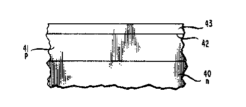
As shown ln FIG. 4, an epitaxial germanium
layer 43 is located upon the surface 42 of a porous
silicon se.~iconductor substrate portion 41. This porous
substrate portion 41 comprises a top p-type portion of a
single crystal n-type bulk silicon semiconductor
substrate 40 ~hich has been made porous at this top
portion, for example, by an anodic reaction with
concentrated hydrofluoric acid. Tl-e anodlc reaction
proceeds faster in p-typ-e than in n-type silicon, as
known in the art~ Such an anodic reaction is described,
for example, in a paper authored by M~I.J. Beale et al.,
entitled "Microstructures and Foundation Mechanism of
Porous Silicon" published in vol. 46, pp~ 85-88 (January
1~86). Ethanol can advantageously be added to the
.. . .
.
~, ::
~ ,:,. . .
undeslraDl~ bubbies during the anodic reaction. The
germanium layer 13 is advantageously grown by ~olecular
beam epitaxy (MBE) upon tne surface of tne porous
substrate after the latter has been suitably cledned.
For exam2le, to clean the surface, the entire substrate
is neated in dry oxy~en to a temperature of about 300
degrees C, to oxidize a surface portion of the porous
silicon; and tnen the substrate is heated in a vacu~
cnamber to a temperature of about 700 to 750 degrees ',
to remove the oxide. Alternatively, the surEace can be
cleaned by oxidizing with a solution of ~lydrogen
peroxide and hydrochloric acid followed by tn~ heating
in tne vacuum chamber. Finally, preferably in the same
vacuum chamber, tne surface of the substrate is
suo~ected to germanium MBE, as known in the art and
àescribed in more detail, for example, in a paper
authorea by J. C. Beant entitled "~lolecular Beam ~pitaxy
of Gex ~ X/ (Si, Ge) Strained-layer Heterostructures
and Superlattices" published in Materials Research
Soci~ Symposla Proceedings, Vol. 37, pp. 245-254
(19~5).
'rhe epitaxial layer 43 and the porous silicon
layer 41 can then ~e patterned into relatively larg_
area(s) as lndicated in FlGo 5, whereby portions of the
silicon substrate 40 are exposed. Then, one or more
opto-electronic elements or devices can be fabricated in
the remaining epitaxial layer 53, with very large scale
integrated (VLSI) circuitry being fabricated ana
integrated in tne exposed portions of the silicon
substrate 40 as known in the art. These opto electronic
aevices and the integrated circuitry can then be
electrically interconnected, illustratively, by
metallization lines 55 and 56. Typically these lines
take the form of aluminum or other suitable metal lines
that are insulated from tne substrate 40 and from the
epitaxial layer 53 by insulating layers (not shown)
except at contact areas of the respective devices anà
~,
except at contact areas of tne respective devices and
circuits through windows in the insulating layers as
known in the art. Alternatively, the epitaxial layer
could be originally grown upon only a limited portion of
the surface of tne substrate. ~lso, instead of, or in
adaition to, having opto-electronic devices fabricated
in the epitaxial layer 53, electronic circuitry can be
fabricated in this epitaxial layer, whereby during
operation in data processing systems, the circuitry in
the epitaxial layer is allocated the task of pèrforming
the more critical data calculations, i.e., the
calculations that are desirably to be performed with
greater speed.
To understand better the underlying principles
of the invention, it is useful to turn to FIGSo 1~ 2 and
3. Here, upon a single crystal substrate 10 havlng a
castellated surface, an epitaxial layer 15 ~FIG. 3) has
been yrown, witi- tangential stress (caused by lattice
mismatch) in the layer at its interface with the
substrate indicated by the arrows in FIG~ 3. The
castellated surface is characterized by flat plateaus 11
(~IG. 2), each of lateral extent 2L, and valleys 12,
each of the valleys having vertical sidewalls 13. The
valleys 12 have bottom surfaces 12 of lateral extent
2S G. Note that the lengths of the arrows are relatively
long at the edges of the plateaus in the immediate
vicinity of the valleys and are relatively short near
the midpoints of the plateaus, indicating relatively
large tangential stress at the edge of the plateaus near
the valleys and relatively small stress near the center
of the plateaus.
The lateral extent G of the gaps, in
accordance with one of the criteria of the invention,
should be sufficiently larye so that the strain fields
that propagate through the epitaxial layer 15 from the
strain sources on different plateaus do not interfere,
i.e. r superposition of strain fields stemming from
. ~ ,- '
': ~: " :- .'
-: ,.. , .
.... .
,;,.'
7 --
separate strain sources is not substantial.
Consequently, tne physical solution to the resulting
boundary value problem involving the establishing of
strain thro~ghout the epitaxial layer is characterized
by exponentially decreasing values of strain as a
function oE distance from the interface. Thus, the
strain enerCJy per unit area of t~e epltaxial layer will
be finite for any arbitrary thickness, no matter how
large. Moreover the strain, energy decreases with
decreasing lateral extent 2L of the plateaus so that for
sufficiently small maximum lateral extent 2L of the
plateaus, tlle strain energy will never exceed the
threshold energy for the formation of dislocations. In
particular, if 2L of plateaus on a surace of Si is less
than about 200 Angstrom, then the pure Ge epitaxial
layers will not have any dislocations regardless of how
thick the layer may be. I~ the lateral extent 2L of the
plateaus of Si is somewhat larger, then the pure Ge
epitaxial layer will still be dislocation-free provided
~0 that its thickness is not too great. In such a case,
the critical layer thickness for dislocation-free growth
of pure Ge upon Si would be finite but greater than that
(10 Angstrom) predicted for growth upon unpatterned
(smooth) Si.
Various modiEications are possible. For
example, instead o~ pure Ge, the dislocation-~ree
epitaxial layer can be Gexsil-x~ ~ith concomitant
somewhat larger allowed values o~ lateral plateau extent
2L depending upon x,or it can be gallium arsenide. More
generally, the su~strate and epitaxial layers can be any
lattice-mi s!na tched crystals, semiconductors or non-
semiconductorsO For example, within the scope of the
invention are binary, ternary, or quaternary III-
~compound semiconductor alloys--generally, (In, Ga, Al)-
(As, P)--grown epitaxially upon lattice-mismatched
su~micron-patterned III-V single crystal substrates--
such as GaAs, InP, or GaP. Note that GaP is only 0
.
~.7~t~.7
lattice mismatcl~ed to Si an~ hence is more nearly
perfectly lattice-matched to Si than are other III-V
compound semiconductors, but by itself GaP has an
in~irect gap and is not as useful for optical devices.
Thus, also within the scope of the invention is the
gro.~th of any III-V lattice-mismatched ~with respect to
GaP) material upon, for example, a submicron patterned
~aP layer which, in turn, has been epitaxially yrown
upon a smooth (unpatterned) surface of a silicon
su~strate.
. ,~, . . .
'.. ~ .