Note: Descriptions are shown in the official language in which they were submitted.
BACKGROUND OF THE INVENTION
Field of the Invention
The present invention is directed to a circuit
arrangement for serial data transmission between a plurality
of subscriber stations, comprising at least two data
transmitters having their output terminals connected to one
and the same data bus which comprises two~leads, and each
having a control input connected to a control arrangement
and being controllable by such control arrangement that, at
most, one of the data transmitters is activated at a given
time, whereby, in their activated condition, the data
transmitters respectively output a voltage of a first polarity
or of a second polarity to the data bus dependent on the
state of a data signal applied to their input, whereby the
data transmitters ha~e a higher internal resistance at the
output in the passive condition than in the active condition,
and whereby at least one data receiver is cannected to the
data bus, the data receiver assuming, in the manner of a
differential amplifier, one of two prescribed signal states
at its output given an existing input voltage and dependent on
its polaritv.
Description of the Prior Art
An arrangement of the type set forth above is
generally known from the periodical "Elektronik", 6/23 March
1984, page 24 and 12/15 June 1984, pp. 97 and ~8.
The known circuit arrangement contains interface
modules for serial ~ransmission, each of which is composed of
a data transmitter and a data receiver and is suitable for
full-duplex or half-duplex operation. In half-duplex
-- 1 --
operation, the output of the data transmitter is directly
connected to the input of the data receiver in every subscriber
station. The subscriber stations which can be a computer
and peripheral devices connected thereto, for example, are
connected to a data bus. The data transmitter and the data
receiver in each subscriber station can be driven into an
active condition or into a passive condition by control
signals.
Since the transmitters, in their active condition,
represent a low-impedance voltage sourc~ at their outputs,
whose voltage is dependent on the logic level o the data
signal applied to the respective input, only one data
transmitted can be activated at a given time~
To this end, a control signal that drives the data
transmitter of a subscriber station into its active condi~ion
can be transmitted to all other subscribers and can be used
at such other subscribers to make an activation impossible for
the time in which the data bus is occupied. It is thereby
obvious to transmit the control signal via control lines or
via a control bus that is provided in addition to the data bus.
SU~ARY OF THE INVE~TION
It is therefore the object of the present invention
to provide a circuit arrangement of the type generally set
forth above such that a mutual control of ~he subscriber
stations occurs via the data bus without the assistance of
additional control lines, this being accomplished such that
the subscriber stations can access the bus on their own when
the bus is not occupied by another subscriber station.
369C3
Given a circuit arranyement of the type general].y
set forth above, all data transmitters are high-impedance
at their outputs given an unoccupied data bus. Proceed.ing
from the perception within the scope of the invention that
this high-impedance tristate condition is exploitable for
control purposes, the circuit arrangement of achieving the
above object is particularly characterized in that the data
bus is provided with a resistor arrangement at at least one
location, each lead of the data bus being connected to a
voltage source via a resistor with the assistance of the
resistor arrangement, and in that at least one of the control
arrangements is preceded by a recognition circuit whichl given
at least approximately identical voltages at all of the leads
of the data bus, outputs a free signal having a first logical
state at its output and, given different voltages at the lines
of the data bus, outputs a busy signal, having a second logic
state, to the control arrangement. The data transmitters can
thereby be connected to the subscriber stations in an
unmediated or a mediated manner, particularly by wa~ of
transmission devices that are provided with modems.
The resistances of the resistor arrangemen~ are to be
dimensioned such that the arrangement defines the potentials
of the data lines at at least one active data transmitter and
the voltage source defines the potentials of the data lines in
the case of exclusively passive data transmitters. When the
data line is provided w.ith terminating impedances of the size
of the characteristic impedance of the data line in view of a
high bit rate of the data signal to be transmitted, then the
resistances of the resistor arrangement are to be dimensioned
adequately low-impedance in comparison to the terminating
impedances but as high-impedance as possible within this
framework. When no terminating impedances are present, the
resistances of the resistor arrangement are to be dimensioned
adequately low-impedance ln comparison to the parallel
connection of the leakage resistances of the modules connected
to the data bus.
An advantage which arises on the basis of the afore-
mentioned measures is that the subscriber stations can acquire
information concerning the occupancy of the data bus with
devices that are simple to realize without a separate control
bus being required for that purpose. With particular
advantage, the busy signal can be used for the control of one
or more modems such that the transmitter of the modem or,
respectively, the transmitters of the modems are driven into
the active condition or the passive condition dependent on the
occupancy of the data bus. When a modem seizes the data bus,
then the data transmitters of all other modems are automatically
activated without switch-over devices comprising involved
control devices being required for that purpose.
In particular, a relay can serve as a recognition
circuit, the winding of the relay being connected to the two
leads of the data bus and the relay responding when the
transmitter is active.
A circuit arrangement for serial data transmission,
as set forth above, has the characteristic that, given an
occupied data line, both leads have at least approximately the
same potential, i~e. the voltage relative to a reference
potential. In accordance with a further feature of the
-- 4 --
3~
invention, this characteristic can be advantageously exploited
in that the circuit arrangement is fashioned and is
particularly characterized in that the recognition circuit
contains evaluation devices for evaluating the voltages
carried by the two leads relative to the reference potential,
and in that, given the voltage level defined by the resistor
arrangement, the evaluation devices form an output signal of
a first type and form an output signal of a second type given
the first prescribed voltage or given the second prescribed
voltage, and in that the output signal of the evaluation
devices are logically operated in the recognition circuit that
the busy signal is formed given at least one output signal of
the second type.
A significant advantage of the foregoing structures
is that the recognition circuit can be composed of electronic
circuits of a standard type. In particular, Schmitt triggers
having a following NAND gate can be employed.
When the data transmitters are of such a nature that
they have a positive voltage in comparison to the reference
potenti~l or, respectively, ground at the one input ~erminal
and havea negative potential in comparison thereto at the
other output terminal, the resistor arrangement can be applied,
for example, to the reference potential as an auxiliary voltage.
When one of the two voltages that the output terminals of the
data transmitters can assume is selected as an auxiliary
voltage, then a greater spacing between the two voltages to be
interpreted occurs, so that these voltages can be more easi].y
distinguished from one another.
- 5
~ ~73~
On the other hand, there are data transmitters that,
in their activated condition, have a first prescribed voltage
at one of the two output terminals and a second prescribed
voltage, higher than the first voltage and of the same
polarity relative to the reference potential, at the other
of the two output terminals, so that differently-polarized
output voltages likewise occur. Data transmitters of inter-
face modules that are conceived for the interfaces RS 485,
RS 422 or the like are, in particular, of this type. The
interface RS 485 is known for half-duplex operation via a two-
wire bus and the interface RF 422 is known for full-duplex or
half-duplex operation via a four-wire data bus.
When such data transmitters and a voltage that is
at least as high as the higher of the two voltages is used as
an auxiliary voltage in a circuit arrangernent of the type set
forth above in which the recognition circuit that contains
evaluation devices for evaluating the voltages on the two leads
relative to the reference potential, then it follows that,
given an occupied data bus, one of the two leads of t~he da~a
bus always lies at the lower of the two prescribed voltages
and, given an unoccupied data bus, both leads are charged with
the higher of the two voltages. Advantageously occurring as a
result thereof is that a single logic element can be provided
as a recognition circuit, this logic element having its inputs
connected to the leads of the data bus, upon in~erposition of
level converters as warranted. In particular, the logic
operation is such that the busy signal is formed given an out-
put ~ignal of the second type.
Advantageously, the circuit arrangement is
constructed in such a manner as to be characterized in tha-t
the vol~age of the voltage source to which the resistors of
the resistor arrangement are connected is higher than the
higher of the two prescribed voltages and in that the control
signal receiver is formed by a logic element connected to the
data bus, the logic element belonging to a circuit family
wherein the lower of the two prescribed voltages corresponds
to one logic state and the higher of the two voltages corre-
sponds to the other logic state.
When the data transmitters belong to circuits for
interfaces of the type RS 4~5,RS 422 or the like, logic
elements in complementary-metal-oxide-semiconductor (CMOS)
technology can be advantageously employed, in particular with-
out having level converters, Schmitt triggers or the like
preceding them. On the other hand, a recognition ci.rcuit
comprisiny an OR gate composed of two diodes and having an
inverter connected thereto via a transistor stage offers the
possibility of adapting the response threshold of the
recognition circuit to the specific conditions of the respective
application on the basis of a suitable selection of the supply
voltage provided for the transistor stage. In particular, a
response threshold that differs only slightly from ground or,
respectively, a reference potential can be realized in this
manner.
With a circuit arrangement of the type set forth
above which is particularly characterized in that a plurality
of resistor arrangements are provided and in that the
respective resistors in the resistor arrangements are
-- 7 --
~3~
connected to the voltage source via a diode which conducts
the voltage of the vo].tage source, the advantage arises that
an outage of the auxiliary voltage, where the voltage decreases,
for example, to the value zero, does not deteriorate the
function of the circuit arrangement for serial data trans-
mission. In particular, a busy state can thereby not be
simulated.
A subscriber station dare not access the data bus
when it has already been occupied by another subscriber. ~hen
a subscriber station has seized the data bus, the recognition
circuit recognizes the same, In this case, however, the data
bus continues to be available to the subscriber station.
When the subscriber station itself does not contain
a device that prevents a self-disconnection of the subscriber
station in the operating state under consideration, then it is
advantageous to forward a busy signal to the subscriber station
only when the data bus is occupied by a different subscriber
station.
Since the data transmitters in the subscriber
stations are activated with the assistance of control signals,
these control signals make criteria available regarding whether
an identified occupation of the bus may possibly occur from
th~ appertaining subscriber station itself. A common
evaluation or logic operation of the control signal and of the
busy signal therefore allows a determination regarding whether
the data bus is occupied by the appertaining subscriber station
or by some other subscriber station. For this purpose the
circuit arrangement is particularly characterized in that a
control input of the subscriber station preceding the assigned
3~
data transmitter i.s respectively preceded by an AND gate
which has a first input connected to the recognition circuit
and a second input, together with the appertaining data
transmitter, is controllable by the subscriber station such
that the AND gate is initialized only given a passively-
driven data transmitter.
Dependent on the type of control circuit with or
without following negation, the AND circuit inhibits the
signal "data bus occupied" when the appertaining subscriber
station itself seized the data bus.
An arrangement that advantageously eliminates
disturbances or, respecti~ely, needle pulses arising due to
switching events is particularly characterized in that the
output of the logic element is connected to a Schmitt trigger
via an RC element so that the Schmitt trigger thereby
simultaneously serves as the AND gate.
With the Schmitt trigger constructed as an AND gate,
the advantage arises that the Schmitt trigger simultaneously
eliminates disturbances and realizes the desired AND operation
or, respectively, NAND operation.
BRIEF DESCRIPTION OF THE DRAWINGS
~ . . ~
Vther objectsl features and ad~antages of the
invention, its organization, construction and operation will
be best understood from the following detailed description,
taken in conjunction with the accompanying drawings~ on which;
FIG. 1 is a schematic circuit diagram of a circuit
arrangement for serial data transmission between a plurality
of digital and transmission assemblies connected to one
~'73~
another via a data bus and comprising a resistor arrangement
connected to the data bus and having recognition circuits
containing NAND gates;
FIG. 2 is a schematic circuit diagram of a circuit
arrangement for serial data transmission wherein each
assembl~ contains its own resistor arrangement, shown as an
excerpt;
FIG. 3 is a schematic circuit diagram of a
recognition circuit comprising an EXCLUSIVE OR gate;
FIG. 4 is a schematic circuit diagram of a circuit
arrangement for serial data transmission in which each assembly
contains a resistor arrangement connected to a negative
auxiliary voltage; and
FIG. 5 is a schematic circuit diagram of a
recognition circuit which comprises two diodes and a transistor.
DESCRIPTION OF THE PREFERRED _EMBODIMENTS
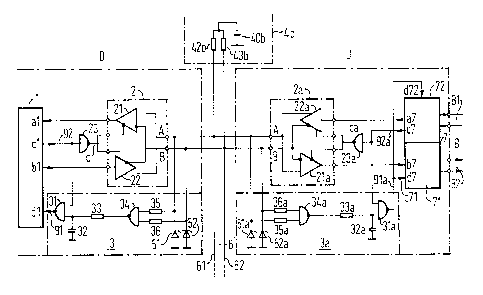
FIG. 1 shows a circuit arrangement for serial data
transmission. The two-lead bus 6 connects a plurality of
assemblies of a remote control apparatus or of a remote control
device, the digital assembly D and t~e transmission assembly U
thereof being illustrated in FIG. 1. In addition to be used
for data transmission, the two leads 61 and 62 of the data bus
6 are also used for the communication of control signals that
serve for the mutual control of the assemblies.
The digital assembly D is a device for executive
sequencing and, as a subscriber station 1 contains a USART 1
controlled by a microprocessor, an interface module 2 and a
~ 10 --
~73~
signal receiver 3.
The transmission assembly U comprises a modem 7
connected to a four-wire audio frequency transmission line 8
which comprises a transmitter 71 and a receiver 72, and
further comprises an interface module 2a and a recognition
circuit 3a. The modem 7 is composed, for example, of an fm
transmitter and an fm receiver. The audio frequency trans-
mission line 8 leads to at least one further subscriber
station and is a component part of a remote control ne~work
comprising a plurality of stations or, respectively, further
subscriber stations in the example set forth herein. The
transmission line is a four-wire line composed of the incoming
line 81 and the outgoing line 82. A two-wire line can be
employed, when warranted, instead of the four-wire line. In
this case, the transmitter 71 and the receiver 72 are to be
connected to the two-wire line.
Further digital and/or transmission assemblies can
be connected to the two leads 61 and 62 of the bus 6. In
particular, such further digital assemblies can be de!vices for
status ~ignal input or output. Further transmission assemblies
can serve the purpose of forwarding the serial data output onto
the bus 6 by a digital assembly or by a transmission assembly
to urther transmission lines and stations connected thereto.
An interface suitable for such a multipoint bus
configuration ser~es as the interface between the assemblies
and the data bus 6, the data transmitters 22 or, respectively,
22a in such an interface and is high-impedance at the output
in the unacti~ated condition. In particular~ the interface
RS4B5 is such an interface.
3~90
In a departure from FIG. 1, the data bus 6 can
be terminated at both ends by a respective resistor between
the two leads 61, 62 which has the characteristic impedance
thereof.
All subscriber stations are connected at a common
ground potential via a connection to ground that is not shown
on the drawing.
For connection to the data bus 6, the assemblies
(of which the drawing illustrates one digital assembly D and
one transmission assembly V) are each provided with a
respective interface module 2 or, respectively, 2a which, for
example, can be of the type SN75176a.
In the interface module 2 of the digital assembly D,
the output terminals A and B of the data transmitter 2 are
directly connected to the input of the data receiver 21. The
terminal A is connected to the lead 61 and the B is connected
to the lead 62 of the data bus 6.
The data transmitter 22 and the data receiver 21
each have their control terminals connected to a common control
line C and can be alternately driven active and passive by
control signals, so that only the data transmitter 22 or the
data receiver 21 can be respectively active at one and the
same time.
The interface module 2a of the transmission assembly
U is constructed like the interface module 2 of the digital
assembly D. The output of the data transmitter 22a is
directly connected to the input of the data receiver 21a. The
data transmitter 22a and the data receiver 21a each have
- 12 -
their control terminals connected to the a common control
line Ca.
The interface module 2 of the digital assembly D
is connected to the USART device 1. The interface module 2a
of the transmission assembly U is connected to the modem 7.
The interface modules 2 and 2a represent level
converters that are operated with TTL levels at that side
facing away from the data bus 6. Depending on the logic state
of the T~L logic level applied to the control line C, however,
the data receivex 21 in the interface module 2 is activated
and the data transmitter 22 is passive, or vice-versa. In a
corresponding manner, the data receiver 21a at the interface
2a is activated and the data transmitter 22a is passive, or
vice-versa, dependent on the logic level of the control si~Jnal
applied to the control line Ca.
On the other hand, it can be advantageous in the
digital assembly D to control only the data transmitter 22 via
the control line C and to always leave the data receiver 21
switched on. Therewith, the data signal transmitted onto the
bus 6 by the digital assembly D can be simultaneously
evaluated for supervision.
In the digital assembly D, the output of the data
receiver is conducted to the data input al of the USART device
1. The input of the data transmitter 22 is connected to the
data output bl of the USART device 1. The control input of
the data receiver 21 and the control input of the data trans-
mitter 22 are directly connected to one another and to the
control line C. The control output cl of the USART device is
connected via the inverter 23 to the control line C of the
~736~
interface module 2.
A resistor arrangement 4b is connected to the data
bus 6. A series circuit comprising a pair of resistors 42b
and 43b of the resistor arrangement 4b is connected between
the two leads 61 and 62 of the bus 6. The junction of these
resistors is connected to the positive pole ~f the auxiliary
voltage source ~Ob which outputs an auxiliary voltage UH. The
negative pole o~ the auxiliary voltage source 4Ob is connected
to ground.
The recognition circuit 3 of the digital assembly 1
D contains a NAND gate 34 whose inputs are connected to the
leads 61 and 62 of the data bus 6 via a respective resistor 35
or 36. The output of the NAND gate 34 is connected to the
signal input of a Schmitt trigger 31 via an RC element
composed of a resistor 33 and a capacitor 32. A control input
of the Schmitt trigger 31 is connected to the control output
cl of the USART device 1.
The two inputs of the Schmitt trigger 31 are linked
to one another in a manner of an AND gate. The inverting
output of the Schmitt trigger 31 is connected to the control
input dl of the USART device 1 via the control line 91.
The digital assembl~ D further comprises an arrange-
ment for protection against overvoltages on the data bus 6.
This arrangement is composed o~ the Zener diode 51 connected
between the lead 61 and ground of the Zener diode connected
between the lead 62 and ground.
The control signal receiver 3a of the transmission
assembly U comprises a NAND gate 34a whose inputs are connected
to the leads 61 and 62 of the data bus 6 by way of respective
- 14 -
3L2~3~
resistors 35a and 36a. The output ~ the NAND gate 34a is
connected to the signal input of the Schmitt trigger 31a via
an RC element composed of the resistor 33a and the capacitor
32a. A control input of the Schmitt tri~ger 31a is connected
to the control output c7 of the modem 7.
The two inputs of the Schmitt trigger 31a are linked
to one another in the manner of an AND gate. The inverting
output of the Schmitt trigger 31a is connected to the control
inputs d71 and d72 of the modem 7 via a control line 91a.
The transmission assembly U further comprises an
arrangement for protection against overvoltages on the data
bus 6, this arrangement being composed of a Zener diode 51a
connected between the lead 61 and ground and a Zener diode 52a
connected between the lead 62 and ground.
NAND gates whose inputs exhibit a Schmitt trigger
characteristic advantageously serve as the Schmitt triggers
31 and 31a. In a modification of the illustrated circuit, such
a NAND gate can be replaced by a Schmitt trigger connected to
the RC element and having a following NAND gate that does not
exhibit Schmitt trig~er characteristics at its inputs.
When the remote con~rol station illustrated in FIG.
1 transmits, the transmission data are applied at the output
bl of the US~RT device 1, are converted to the interface level
in the data transmitter 22 of the interface module 22 serving
as a driver, are fed by way of the lines 61 and 62 of the data
bus 6 to the data receiver 21a of the interface module 2a, are
converted to the TTL level by the latter and are output ~o the
input b7 of the transmitter 71 contained in the modem 7.
~.~73~
In the receiving condition of the remote control
station, the received data are applied at the output a7 of
the receiver 72 contained in the modem 7, are converted to
the interface level in the data transmitter 22a of the
interface module, are fed via the leads 61 and 62 of the data
bus 6 to the data receiver 21 of the interface module 2, are
converted to the TTL level by the latter and are output to
the data input al of the USART device 1.
The tristate cGndition of the RS485 data bus 6
corresponding to a logical level "O" on the control line C or,
respectively ~a, signals the connected assemblies that they
car. access the data bus. When an assembly accesses the data
bus 6, then the data bus assumes a non-tristate condition. The
evaluation of this condition leads to the formation of a control
signal in the further assemblies which switches the control
line 91 or, respectively, 91a to the logic level "O" and there-
fore inhibits the access of all other assemblies to the bus.
This control signal also drives the transmission assembly
(assemblies) such that their transmitters 71 become active
toward the transmission lines 8 and such that their receivers
72 are inhibited.
The USART device 1 can be, for example, of the type
SAB 8251 A.
The control of the interface module via the bus 6
comprises the following operating conditions:
a) When the da~a bus 6 is not occupied, i.e~
when all data transmitters 22, 22a are in the
high-impedance tristate condition, then the
two leads 61 and 62 of the data bus lie at
- 16 -
~ ;~73~i9~
positive potential of, in particular, about
UH=12V, lying thereat via the resistors 42b,
43b. Voltage to which the logical level "1"
corresponds, therefore, respectively derive
at the two inputs of the CMOS NAND gates 34
or, respectively, 34a. The outputs of the
NAND gates 34 and 34a therefore have the
logic level "0". The output of the Schmitt
trigger 31 or, respectively, 31a is therefore
switched to the logic level "1", regardless of
the logic level of the control signal fed to its
control input.
In the digital assembly D and, under given conditions
in further digital assemblies, the logic level "1" on the
control line 91 signals the USART device 1 that the data bus
6 is not occupied. In this case, the audio frequency trans-
mission line 8 ~ the remote control networ]~ is also not
occupied. In the transmission assembly and, under given
conditions, in further transmission assemblies~ the logical
"1" on the control line 91a drives the receiver 72 to receive
and inhibits the transmitter 71.
b) When the data bus 6 is seized by the
digital assembly, then, in the seizing of
the digital assembly, control outputs cl of
the USA~T device 1 switches the control line
92 connected thereto to the logic level "0".
The inverter 23 activates the data trans
mitter 22. The output of the data trans-
mitter 22 is therefore in a low-impedance
condition. Dependent on the logic state at
~7;~
the data output bl of the USART device 1,
a logical "1" or a logical "0" is trans-
mitted via the data bus 6.
The two prescribed voltages at the output terminals
A, B of the data transmitters 22, 22a can assume relative to
the reference potential have the same polarity.
In the case of the interface RS 485, the voltage
3.7V for e~ample, is at the output terminal A of the interface
module 2 given a logic level "1" and the voltage l.lV ~o
ground, for examplel lies at the output terminal B. Given a
logic level "0", the voltage l.lV, for example, lies at the
output terminal A and the voltage 3.7~, for example, lies at
the output terminal B. Given an activated interface module
and a bus 6 thereby occupied, one of the two leads 61 or 62
therefore basically lies at the low voltage of, for example,
l.lV. The logic level "0" at the input of the CMOS NAND gate
34 corresponds to this potential. Thi.s con~ition switches the
output of the NAND gates 3~ and 3~a to the logic level "1l'
in all assemblies.
In the active digital assembly D, ~his signal is not
forwarded since the Schmitt trigger 31 is inhibited by a logical
"0" from the control output cl of the USART device 1.
In the operating condition under consideration,
further digital assemblies (not shown on the drawing) which may
be present are not active, by contrast, so tha~ the Schmitt
triggers are opened by a logical "1". The logical "1" at the
output of the NAND gate therefore drives the control line to
the logic level "0" via the following Schmitt trig~er, informs
the USART device that the data bus 6 is occupied ~y another
- 18
~L2~3~
assembly and therefore inhibits access to the data bus 6.
In the transmission assembly U and, under given
conditions, in further transmission assemblies, the logical
"1" at the output of the NAND gate 34a drive the control
line 91a to a logic level "O" via the following Schmitt
trigger 31a therefore inhibits the receiver 72 and switches
on the transmitter 71.
c) When the data bus 6 is occupied by the
transmission assembly U, then the receiver
72 receives a message from the remote control
network via the audio frequency line 8. ~he
control line 92a switches to a logical "O",
therefore inhibits the Schmitt trigger 31a
and activates the data transmitter 22a via the
.inverter 23a so that the data transmitter 22a
works onto the data bus 6. The analogous case
applies to a further transmission assembly in
case this occupies the data bus 6 instead of
the transmission assembly U.
In the digital assembly D connected to the data bus
6, the NAND gate 34 recognizes the busy condition and, with a
logical "O" that proceeds to the control input dl of the USART
device 1 via the control line 91, inhibits the access of the
USART device 1 to the bus 6. The same likewise applies to
further digital assemblies connected to the bus 6.
When further transmission assemblies U are connected
to the bus 6, then their NAND gates 34a recognize the busy
condition and, via the follow~ng Schmitt trigger 31a switch
off the receiver 72 and switch on the data transmitter 71.
-- 19 --
~.~73~
Branching functions in transmission networks can
be realized in an especially simple manner with the assistance
of the control arrangement without having a requirement for
additional logic operations or control signals or control
signal lines between the transmission assemblies.
In a modification of the illustrated arrangement,
it can also be advantageous not to drive the receiver active
or passive dependent on the occupancy of the data bus, but to
always keep it ready to receive in that its control input is
permanently applied to ground potential.
Referring to FIG. 2, a circuit arrangement for serial
data transmission is illustrated which largely agrees with
that of FIG. 1. In a departure therefore, a plurality of
decentralized resistor arrangements 4 and 4a are pro~ided
instead of a single resistor arrangement 4b. Each of the
assemblies connected to the data bus 6 has its resistor
arrangement assiyned thereto, this being preferably accommodated
by the appertaining assembly. The resistor arrangements 4
and 4a are respectively constructed like the resistox
arrangement 4b of FIG. 1.
In the digital assembly D, a series connection
comprising the resistors 42 and 43 of the resistor arrangement
4 applies between the two leads 61 and 62 of the data bus 6.
The junction of the resistors 42 and 43 is connected to the
cathode of a diode 41 whose anode is connected ~o the positive
pole of the auxiliary ~oltage source 40 that outputs the
auxiliary voltage U~. ~he negative pole of the auxiliary
voltage source 40 is connected to ground.
- 20 -
~,~ 7 ~ 6 ~
In the transmission assembly U, a series connection
comprising a pair of resistors 42 and 42b of the resistor
arrangement lies between the two leads 61 and ~2 of the data
bus 6. The junction of the resistors 42a and 43a is connected
to the cathode of the diode 41a whose anode is connected to
the positive pole of the auxiliary voltage souxce 40a that
outputs the auxiliary voltage UH. The negative pole of the
auxiliary voltage source 4Oa is connected to ground.
The exemplary embodiment illustrated in FIG. 2 has
the advantage that no separate assembly is required for the
resistor arrangement.
FIG. 3 illustrates a recognition circuit which
largely coincides with the recognition circuit in the
arrangement of FIG. 2. The only departure is that an
EXCLUSIVE OR gate 37 is provided instead of the NAND gate 34.
This recognition circuit can replace the recognition circuit
3 or, respectively, 3a in the circuit arrangements of FIG. 1
and FIG. 2. The EXCLUSIVE OR element 37 has the advantage
that a positive or a negative auxiliary voltage can be
utilized in the resistor arrangements 4 and 4a. As in the
other exemplary embodiments, the auxiliary voltage must be of
at least approximately the same magnitude in all resistor
arrangements that are connected to the data bus 6.
The portion of the circuit arrangement for serial
data transmission shown in F~G. 4 shows that case wherein a
negative auxiliary voltage -l1H is employed in all resistor
arrangements 4 and 4a instead of a positive auxiliary voltage.
The diodes 41 and 41a are therefore respectively polarized
such that their cathodes lie at the auxiliary voltage -UH.
- 21 -
~.~7~
The recognition circuit illustrated in FIG. 5
contains two diodes and a pnp transistor. The diodes 305
and 306 each have their cathode connected to a lead 61 or,
respectively, 62 of the data bus. The anodes of the diodes
305 and 306 are directl~ connected to one another and are
connected to the base of the transistor 302 via a resistor
304. The transistor 302 has its emitter connected to the
supply voltage +Uv and has its collector connected to ground
via a resistor 303 and directly connected to the input of the
NAND gate 31 via the RC element composed of the series
resistor 33 and the shunt capacitor 32. The NAND gate 31 has
its other input connected to the control line 92. The control
line 91 is connected to the output of the NAND gate 31.
The supply voltage Uv amounts to, for example, 5V.
Two diode thresholds and a resistor are respectively effective
between the leads 61 and 62 of the data bus 6 and ground, in
particular the respective diode threshold o~ the appertaining
diodes 305 and 306 and the diode threshold of the base emitter
path of the transistor 302. Given an occupied data bus, one
of the leads 61 or 62 has approximately ground potential there-
on. The appertaining diode 305 or 306 becomes conductive and
through~connects the transistor 302 which, therefore, assumes
a potential at its collector that corresponds to a logical "1".
The output of the driver 301 outputs the same logic level.
When one or more diodes, polarized such that they
are isodirectionally connec~ed in series with the base-emitter
diode, are inserted between the emitter of the transistor 32
and the supply voltage ~Uv, then the response value of the
recognition circuit can be selected in a comparatively broad
- 22 -
~ \
~3~
range.
Although we have described our invention by
reference to particular illustrative embodiments thereof,
many changes and modifications of the invention may become
apparent to those skilled in the art without departing from
the spirit and scope of the invention. We therefore intend
to include within the patent warranted hereon all such changes
and modifications as may reasonably and properly be included
within the scope of our contribution to the art.
- 23 -