Note: Descriptions are shown in the official language in which they were submitted.
~27459~;
HIGH-SPEED LINK FOR CONNECTING PEER SYSTEMS
1. Field of the Invention
The present invention relates to data processing
6ystem6 and more particularly to systems for
linking component systems together to form a
data processing system.
2. Description of the Prior Art
In the prior art, parallel buses have generally
been used to connect components of a single
computer system and serial links have been used
to link peer systems toqether. The parallel bus
has offered high speed, but has generally
.,., . '
' , '
'
~L27~ 6
presumed that at least some of the connected
components were not peers, i.e., were required
in order for the system to operate at all. The
serial link has been used to connect peer
systems, and consequently could operate as long
as any of the systems connected to it was
operable. Data transmission over a serial link
is, however much slower than over a parallel
bus. What is needed, and what is provided by
the present invention is a link which offers the
high speed typical of the bus together with the
peer relationship of the components typical of
the serial link.
Summary of the Invention
The present invention relates to links for
connecting components of computer systems. The
invention is a high-speed link for connecting a
plurality of peer component systems. Each
component system includes an input-output
system. The link is connected to each
input-output system and includes data lines and
control lines. Included in the control lines
. ' ~ '. ~, ~ .
:'. ' ' ' ' '
,
~274596
are the following types: system status lines
showing status of all connected component
systems to each component system, arbitration
lines for indicating whether the high-speed link
is currently in use and which of the connected
component systems wishes to commence
transmission, and receiver acquisition lines for
specifying which of the component systems is to
receive the transmission and whether the
specified component system is able to receive
it.
The link further includes a device adapter in
each input-output system connected to the data
and control lines. In the device adapter are
included the following: system status detection
logic connected to the status lines for
inhibiting transmission of data to a component
system which is not ready therefor, arbitration
logic connected to the arbitration lines for
determining whether a component system may have
access to the link at any given time, receiver
acquisition logic connected to the receiver
acquisition lines whereby a transmitting
input-output system may specify a receiving
..
~274~;96
input-output system, the specifed system may
acknowledge its selection and ability to
receive, and the transmitting system may verify
that the specified system has been selected and
is able to receive data, data providing logic
responsive to the receiver acquisition logic for
providing data to the data lines after selection
of a receiving system has been verified and data
receiving means in the receiving system
responsive to the receiver acquisition logic for
receiving data from the data lines.
It is thus an object of the invention to provide
improved means for linking computer systems;
It i6 a further object of the invention to
provide a high-speed link for peer systems~
It is another object of the invention to provide
a high-speed link connecting peer systems
wherein each system may determine the status of
the others.
It is an additional object of the invention to
provide a high-speed link wherein a transmitting
., ~ .
~274~9~
system may verify that it has the specified
receiving system and that the receiving system
can receive the data before commencing a
transmission.
Other objects and advantages of the present
invention will be understood by those of
ordinary skill in the art after referring to the
detailed description of a preferred embodiment
contained herein and to the drawings, wherein:
Brief Description of Drawings
Fig. 1 is a block diagram of peer systems
employing the present invention:
Fig. 2 is a detailed logical diagram of the
high-speed link of the present invention;
Fig. 3 is an overview block diagram of an 1/0
system employing the high-speed link of
the present invention;
,, , ~
~274596
Fig. 4 is a timing diagram of the start of a
transmission operation over the
high-speed link;
Fig, 5 is a timing diagram of the normal
termination of a transmission operation
over the high-speed link;
Fig. 6 is a detail of the logic controlling RDY
lines 203 in the high-speed link;
Fig. 7 is a detail of the logic generating clock
signals in the high-speed link;
Fig. 8 is a detail of the bus arbitration logic
in the high-speed link:
Fig. 9 is a detail of the sequencer logic
controlling start of a data transmission
in the high-speed link; and
--6--
- . ' -
~4596
Fig. 10 is a detail of the logic controlling
start of reception of data in the
high-speed link.
Reference numbers in the figures have three or
more digits. The two least-significant digits
are reference numbers within a drawing; the more
significant digits are the drawing number. For
example, the reference number 1003 refers to
item 3 in drawing 10.
DESCRIPTION OF A PREFERRED EMBODIMENT
The following Description of a Preferred
Embodiment will first describe the system of
peer computer systems in which the present
invention is employed, then describe the signals
and timing in the HSL in detail, and finally
describe an I/O processor which operates the HSL
in detail.
--7--
~2~
l. System in which the HSL is employed: Fig. 1
A preferred embodiment of the ~SL is employed in
the loosely-coupled computer system shown in
Fi~ure 1. Loosely-coupled system 102 of that
figure is composed of up to 4 stand-alone
computer systems 103, each one of which
functions as a peer system. Each computer
system 103 includes a CPU 105, a physical memory
(PMEM) 107, and a set of I/O processors (IOPs)
117. Each IOP is connected to one or more
input/output devices. Shown in Figure 1 are a
mass storage device (MS) 119 connected to IOP
117(a) and a group of terminals (TERM) 121
connected to IOP 117(n). The number of IOPs 117
may vary in a system 103, as may the type and
number of I/O devices attached to an IOP 117.
The IOPs 117, CPU 105, and PMEM 107 are
connected by means of system bus 113. Both CPU
105 and individual IOPs 117 have direct access
to PMEM 107 via bus 113.
System 103 in preferred embodiment is a
multiprocess system. Operations performed by a
system 103 are p-reormecl eor the E~rocess which
- 8--
g6
is presently executing on CPU 105. When system
103 performs an I/O operation for a process, CPU
105 places an I/O command word (IOCW) 109
specifying the operation at a location in PMEM
107 known to the IOP 117 which must perform the
operation, signals the IOP 117 that it has an
operation to perform, and ceases executing
instructions for the process that requested the
operation until the I/O operation is complete.
While the I/O operation is being completed, the
process is barred from CPU 105 and CPU 105
executes instructions for another process.
IOP 117 responds to the signal from CPU 105 by
retrieving IOCW 109 from PMEM 107 and performs
the operation specified therein, referencing
PMEM 107 directly as required to read data from
PMEM 107 to an I/O device or to write data from
the I/O device to PMEM 107. When the operation
is complete, IOP 117 places an I/O status word
(IOSW) 111 indicatirg the status of the
operation at a special location in PMEM 107 and
signals an interrupt to CPU 105. CPU 105
responds to the interrupt by executing system
interrupt code which examines IOSW 111 to
determine the outcome of the operation and then
performs the processing required to permit the
process for which the I/O operation was
performed to resume execution on CPU 105. In a
preferred embodiment, systems 103 may be VS
computer systems manufactured by Wang
Laboratories, Inc. Loosely-coupled system 102
may consist of up to four VS computer systems of
the types VS 85, VS 90, VS 100, or VS 300.
Different models may be combined in the same
system 102.
When system 103 is part of loosely-coupled
system 102, one IOP, shown in Figure 3 as HSL
IOP 115, is specally adapted to be connected to
HSL 101 connecting the given system 103 to up to
three other systems 103. Since HSL 101 is
connected to an IOP, a given system 103 can
transfer data to and receive data froM another
system 103 in exactly the same fashion as it
transfers data to and receives data from any
other I/O device.
--10 -
~2~4~96
2. Detailed Description of HSL lOl: Fig. 2
Continuing with a detailed description of HSL
101, Figure 2 presents a high-level overview
thereof. HSL lOl consists of 30 logical lines
connecting system 103(x), which is transmitting
data, and system 103(y), which is receiving
data. Any system 103 connected to HSL 101 may
use HSL lOl to either transmit or receive data.
The 30 logical lines are subdivided into 16 data
lines D 201(0..15), making up data lines 219,
and 14 control lines 221. All lines are
bidirectional. The 16 data lines are used to
transfer packets consisting of a 16-bit message
word followed by a sequence of 16-bit data words
between system 103(x) and 103(y). The message
word contains the HSL address of system 103(x)
and the number of data words in the
transmission.
Control lines 221 may be subdivided into the
following functional groups: the system status
lines, the HSL arbitration lines, the receiver
acquisition lines, the parity lines, and the
1274596
clock line. The system status lines are RDY
203(0..3). Each of these lines corresponds to
one system 103 connected to HSL 101 and
indicates whether that system 103 is ready to
receive data. The HSL arbitration lines are REQ
205(0..2) and BUSY 209. These lines provide
signals which determine which HSL IOP 115 will
use HSL 101 next and will seize the bus for that
IOP 115. The receiver acquisition lines are RA
207, which provides the address of the receiving
HSL IOP 115 to the receiver and receives the
confirmation of that address from the receiver
and ACR 211, which first indicates that the
receiver has received the request and then
indicates whether the receiver is in condition
to receive data.
The parity lines, DP 215 and PAR 213 permit
parity checking to ensure that no error occurred
in transmission of data and message words across
HSL 101. The clock line, XCL 217, finally,
carries timing signals which control the setting
up of a transmission and the transmission of the
data and message words.
`
,
- ' -
127~;96
RDY 203(0..3): These lines are ready lines, one
for each system 103 which may be connected to to
HSL 101. When a HSL IOP 115 for a system 103 is
operating, that system 103's line in RDY 203 is
high. Each system 103 sets its own RDY line and
reads the other ready lines. If a system 103's
ready line falls during a transmission to that
system, the transmission is terminated.
REQ 205¢0..2): These are lines by which systems
103 request use of HSL 101 for transmitting
data. Each request line is assigned to one of
the systems 103, and the line's number
determines the system 103's access priority for
HSL 101. If two systems 103 attempt to transmit
data on HSL 101 at the same time, the one with
the highest access priority is given access to
HSL 101 and the other is excluded. The system
103 having REQ 0 has the highest priority, the
system with REQ 1 the next, and so on. The
lowest priority belongs to the system 103 which
does not have a REQ line 205, and that system
103 may begin transmitting data on HSL 101 only
when no other system 103 is requesting use of
HSL 101.
-13-
'-,'
. . .
~274596
BUSY 209 is received by all systems 103. The
line indicates whether HSL 101 is currently in
use and if it is, inhibits other systems 103
from starting transmission.
RA 207(0..1): These lines carry addresses of
systems 103 on HSL 101. In a preferred
embodiment, there is a maximum of four systems
103, and consequently, addresses can be
expressed in two bits. After a transmitting
system 103(x) has gained access to HSL 101, but
before receiving system 103(y) has accepted
anything on data lines 219, it sets RA 207(0..1)
to the address of the receiving system 103(y).
System 103(y) responds to RA 207 specifying its
address by putting its own address on RA 207.
System 103(x) then compares the address it
receives on RA 207 with the address it
originally specified, and if they differ, system
103(x) abandons the attempt to transmit.
ACR 211 carries acknowledgements from from
receiving system 103(y) to transmitting system
103(x). Receiving system 103(y) sets ACK 211
acknowledging that it has been selected at the
-14-
~''
,
'
~27~96
same time that it sends its address on RA 211.
If receiving system 103(y) cannot receive data,
it later resets ACK 211. Transmitting system
103(x) samples ACK 211 twice before beginning to
transfer data. The first time, it samples to
make sure that ACK 211 has been set, the second
time, it samples to make sure that ACK 211 has
not been reset.
DP 215 transmits the odd parity value for the
message or data word currently being sent on
data lines 219 from system 103(x) to system
103(y). System 103(y) checks the parity of the
message or data word it has received with the
parity value it received for the word via DP
215. If the two do not agree, system 103(y)
sets PAR 213. When system 103(y) sets PAR 213,
transmitting system 103(x) discontinues the
transmission.
XCL 217 is a transmission clock signal which
system 103(x) which has seized HSL lO1 provides
to all other systems 103. XCL 217's signals
synchronize selection of a specific system
103(y) and following that, the transmission
-15--
12~
itself. In a preferred embodiment, the period
of XCL 217 may be adjusted as required for HSLs
101 of various lengths.
HSL 101 is implemented physically as a
60-conductor flat twisted pair cable in which
each twisted pair is a differential pair for one
of the thirty logical lines described above.
Systems 103 connected by HSL 101 are
daisy-chained together, i.e., each system has a
panel with two connectors for the cable.
Connected to the connectors is piece of the
cable with another connector at its center.
This connector is connected to the system 103.
In the first system 103, one panel connector
receives a bus terminator and the other receives
the cable to the second system 103. In the
second system 103, the cable from the first
system 103 is connected to one of the panel
connectors and the cable to the thitd system 103
is connected to the other panel connector, and
so forth. In a preferred embodiment HSL 101 may
employ up to 160 total feet of cable to link
systems 103 into a single system 102. In other
embodiments, XCL 217 may be adjusted to permit
greater cable lengths.
12~74S96
3. Operation of HSL 101: Figs. 4 and 5
Operation of HSL lO1 during a data transmission
between system 103(x) and 103(y) will be
described using the timing diagrams of figures 4
and 5. Figure 4 is a timing diagram of the
start of a transmit operation. Beginning at the
top, DACLK represents a clock signal internal to
HSL IOP 115 for system 103(x), henceforth HSL
IOP 115(x). XCL 217 is derived from DACLK, and
it is DACLK whose period is adjusted as required
by the length of HSL 101. DAGRANT is another
signal internal to HSL IOP 115(x) which is
produced by grant logic which determines from
the values of RFQ 205(0..2) and BUSY 209 whether
system 103(x) may access HSL 101. As seen in
Fig. 4, DAGRANT in a preferred embodiment goes
high when system 103(x) has access. The
remaining signals in the timing diagram are
those carried on the lines of HSL 101.
Before starting a transmission, HSL IOP 115(x)
checks whether RDY 203(y) for receiving system
103(y) is high. If it is, HSL IOP 115(x) sets
REQ 205(x) for transmitting system 103(x) low,
-17_
.. . .
. . ~ . , , ' .
'. ' ~ ' -
~4~
indicating a request from system 103(x). The
grant logic responds to the states of BUSY 209
and the REQ 205 lines for the other systems
103. If BUSY 209 is low, indicatinq that HSL
101 is free and the REQ 205 lines indicate that
system 103(x) has priority, the grant logic
delays 8 DACLK periods to allow for propagation
delay and then permits signal DAGRANT to go
high. One DACLK period before DAGRANT goes
high, system 103(x) puts the message word onto
data lines 201. In response to DAGRANT, REQ
203(x) goes high and BUSY 209 goes high, seizing
HSL 101 for system 103~x).
One DACLK interval after the bus has been
seized, HSL IOP 115(x) gates the HSL address of
recelving system 103(y) onto RA(0..1) 207. Two
DACLK intervals later, HSL IOP 115(x) produces a
pulse, XCL(l), on XCL 217. At the end of that
DACLK interval, HSL IOP 115(x) ceases gating the
adress of system 103(y) onto RA 207. That
address appears in Figure 4 as XRA. In response
to XCL(l), HSL IOP 115 of system 103(y),
henceforth HSLIOP 115(y), reads RA 207, compares
the address therein with its own address, and if
..~
-18-
~2~74~g6
they are the same, produces an internal receive
enable signal, RCV EN on the next clock. In
response to RCV EN, HSLIOP 115(y) sends its own
address (RRA in Figure 4) on RA 207 and raises
ACR 211, indicating that it has been selected to
receive.
After sending XRA, HSL IOP 115(x) waits five
DACLK intervals to permit time for XRA to
propagate to HSL IOP 115(y) and for RRA and the
ACK signal to propagate back to HSL IOP llS(x).
Thereupon, HSL IOP 115(x) produces XCL(2). In
the next DACLR interval thereafter, it puts the
first data word of the packet being transmitted
onto D 201. At the same time, HSLIOP 115(x)
samples RA 207 and ACK 211, as indicated by RRAS
and ACKS1 respectively. HSL IOP 115(x) compares
RRA with the address which it sent in XRA in the
next DACLX cycle. If they are not the same or
if ACK 211 is low, indicating that HSLIOP 115(y)
is not empty and therefore cannot receive data,
HSL IOP 115(x) terminates the transmission by
lower;ng BUSY 209. If HSLIOP 115(y) can receive
data, it responds to XCL(2) by clocking MW into
a register.
-19--
.
,: ' ' '
~2~
If HSL IOP 115(x) has not terminated the
transmission in response to RRA or ACR 211, it
waits five DACLK intervals after XCL(2) in order
to permit the signal on ACX line 211 to
propagate back to HSL IOP 115(x). It then
samples AC~ line 211, and if it is low (shown in
dashed lines in figure 4), terminates the
transmission. If the transmission is not
terminated, HSL IOP 115(x) produces XCL(3) and
the following XCL pulses, one for each DACLK
interval. Each pulse is accompanied by a data
word on D 202, and HSL IOP 115(y) receives the
data word in response to the XCL pulses.
As mentioned in the discussion of DP line 215,
each time HSL IOP 115(x) transmits a message or
data word, DP 215 indicates the word's parity.
In a preferred embodiment, the indicated parity
is odd. HSL IOP 115(y) receives the parity
signal on DP 215 together with each transmitted
word. HSL IOP 115(y) checks the parity of each
received word and compares the result with the
signal received on DP 215. If both do not show
the same parity, HSL 115(y) raises PAR 213, and
in response thereto, HSL IOP 115(x) terminates
_20-
~27~S96
the transmission. In figure 4, the dotted lines
on PAR 13 show a response to a parity error in
MW, the message word~
Continuing with figure 5, that figure shows the
timing for the termination of a transmission.
Termination may be either because all of the
data words in the packet have been transmitted
or because RDY 203(y) went low or PAR 213
indicated an error. When the termination is
normal, i.e., because all of the data words have
been transmitted, XCL 217 ceases producing
pulses after the last word sent prior to
termination is on D 201. HSL IOP(x) then waits
6 DACLK pulses to ensure that the last word sent
and DP 215 for the word have propagated to HSL
IOP(y) and any signal on PAR 213 indicating a
parity error has propagated back and lowers BUSY
209, releasing HSL 101. When the termination
occurs because RDY 203(y) went low or PAR 213
indicated an error, BUSY goes high the next
DACLK tick after the error is detected in HSL
IOP(x).
. ' '
~ ' '
- .
~27~;96
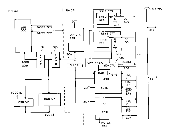
4. Overview of HSL IOP 115: Fig. 3
In a preferred embodiment, HSL 101 is controlled
by HSL IOP 115. Figure 3 is a high-level block
diagram of HSL IOP 115. HSL IOP 115 contains
two main subsystems: I/O controller (IOC) 301,
which controls operation of HSL IOP 115 and
device adapter (DA) 321, which performs the
actual transfer of data between HSL IOP 115 and
PMEM 107. Beginning with IOC 301, IOC 301 has
two main buses: bus 113, which connects it to
PMEM 107 and CPU 105, and IOP bus 309, which
connects it to DA 321. IOC 301 controls its own
operation and that of DA 321 by means of
microprocessor system (uPS) 303. Included
therein are a microprocessor and the attendant
program and data memories. uPS 303 is connected
to IOPB 309 and can read and write the contents
of other devices connected to IOPB 309. To read
and write, uPS 303 provides addresses as
indicated by IADDR 305. Information by which
uPS 303 controls operation of DA 321 flows
between uPS 303 and DA 3Zl by means of control
signals (DACTL) 307 and by means of IOPB 309.
IOPB 309 carries instructions from uPS 303 to DA
1274~g6
321 and status information from DA 321 to uPS
303.
Bus 113 is connected via DAR 317 to IOPB 309.
DAR 317 contains registers used for transferring
data between bus 113 and DA 321 and for
addressing the locations in PMEM 107 which are
the source or the destination of the data being
transferred by IOP 115. The data transfer
registers include separate sets for data
received in IOP 115 and transmitted from IOP 115
and the address register includes logic for
incrementing the address. XCVRs 311 and 313,
which operate under control of uPS 303, permit
data to be transferred between DAR 317 and uPS
303 or DA 321.
Control and status register (CSR) 315 contains
three kinds of information: IOP control
information, bus control information, and IOP
status information. The IOP control information
determines what operation IOP 315 is to perform
and is received from IOCW 109 defining the
operation. The bus control information is
information by which CSR 315 controls operation
,
~L2~4596
of bus 113 when it is reading data from or
transferring it to PMEM 107. The IOP status
information indicates the current status of IOP
115. The information contained therein is
provided at the end of an operation to IOSW 111.
Continuinq with DA 321, DA 321 is connected by
IOPB 309 to DAR 317 and uPS 303 and to HSL 101
by HSL interface (HSLI) 327, which, in a
preferred embodiment, consists of differential
drivers and receivers connected to the paired
lines in HSL 101. In figure 3, HSLI 327 is
divided into two halves, one for data lines 219
and the other for control lines 221. Connected
to the half for data lines are transmit system
(XSYS) 323 and receive system RSYS 337. XSYS
323 is connected to IOP~3 bus 309, whence it
receives the data to be transmitted, and to DO
329, whereby it provides the data to HSLI 327.
In XSYS 323, X latch (XL) 326 stores the next
word to be put out to lines 219, while XRAM 325
stores the data words in a packet. XSYS 323
further contains an address counter used to
generate addresses for XRAM 325 and a data word
counter used to count the number of data words
-24_
', ' ' ~ ~
.. . .
1274596
transferred from XRAM 325 to data lines 219.
The data counter is loadable and readable by uPS
303.
RSYS 337 receives data from ~SLI 327, to which
it is connected by DI 331, and provides it to
IOPB 309. In RSYS 337, message latch ~ML) 336
receives and holds the message word with which a
packet begins, while RRAM 335 stores the data
words received in the packet. RSYS 337 has an
address counter which is readable by uPS 303.
XSYS 323 and RSYS 337 are separately controlled,
and consequently, it is possible to load XRAM
325 from IOPB 309 while RRAM 335 is receiving
data from DI 331 and vice-versa.
Direct memory access control (DMA CTL) 339
controls the transfer of data words between DAR
317 and XSYS 323 or RSYS 337 in response to
signals of DACTL 307. Included in DMA CTL 339
is a counter which terminates a data transfer
after a specified number of words have been sent
or received. When data is being transmitted,
the number comes from IOCW lO9: when it is being
received, it comes from the packet's message
-25-
~274596
word. The separate control of XSYS 323 and RSYS
337 mentioned above makes it possible to perform
a DMA operation on XRAM 325 or RRAM 335 while
the other RAM is being used to transmit or
receive data. uPS 303 sets the counter in
DMACTL 339 and provides the signal which starts
a transfer operation. SB 341 is a buffer which
contains status information about DA 321 and is
readable by uPS 303.
RDYCTL 345 reads RDY 203 lines from other
systems 103 and sets the state of its own RDY
203 line. The values of the lines read by
RDYCTL 345 are output to SB 341, while RDYCTL
345 sets its own RDY 203 line in response to an
instruction received on IOPB 309 from uPS 303.
The parts of DA 321 which respond to and produce
signals on control lines 221 are XCTL 349, which
controls transmission of a packet, and RCTL 353,
which controls reception of a packet. XCTL 349
and RCTL 351 are further responsive to signals
in DACTL 307 and respectively produce XCTL
signals XCTLS 343, which control XSYS 323, and
RCTLS 353, which control RSYS 337. Arrows
1:27~;9~i
connecting XCTL 349 and RCTL 351 with HSLI 327
indicate which control lines affect operation of
the respective component and whether the
component produces signals on the lines,
consumes them, or both. Thus, XCTL consumes RDY
203, ACK 211, and PAR 213, produces DP 215 and
XCL 217, and both produces and consumes REQ 205,
BUSY 209, and RA 207. XCTL 349 further includes
RAD 348, a latch loadable from IOPB 309 which
contains the address of the destination of a
transmit operation.
5. Operation of HSL IOP 115
HSL IOP 115 performs a transmit operation in
three steps: first, transmitting HSL IOP 115(x)
determines whether receiving system 103(y) is
ready and if it is, sets up the transmission.
HSL IOP 115(x) next performs a DMA operation
loading one paoket of the data to be transmitted
from PMEM 107 into XRAM 325. Finally, XCTL 349
seizes HSL 101 and transmits the data. If more
data is to be transmitted than is contained in
one packet, the second and third steps are
' "'' ~ ' ; ~ ~"
, - :
~2~g~
repeated until the specified amount of data has
been tranmitted.
Before HSL IOP 115 can begin operation, a
program executing on system 103(x) must prepare
an IOCW 109 for the operation at a special
memory location known to HSL IOP 115 and execute
a SIO ~start I/O) instruction specifying system
103(y). In response to the SIO instruction, CPU
105 places a signal for IOP 115 and a value
indicating the destination system on bus 113.
In response to the signal, uPS 303 latches the
value indicating the destination system into CSR
315 and then issues a command to bus 113 to
fetch IOCW 109 from PMEM 107. IOCW 109
specifies the I/O operation, the address in PMEM
107 at which the data to be transferred is
stored, the number of words in the data, and the
HSL bus address of the destination. uPS 303
first reads SB 341 to determine whether
destination system 103(y) is ready. If it is
not, uPS 303 makes an IOSW 111 indicating that
fact, places it in PMEM 107 at a location
associated with system 103(x) and generates an
interrupt to CPU 105. If it is, uPS 303 places
~2~74~;96
the memory address specified in IOCW 109 in the
memory register of DAR 317 and places the kind
of operation, the number of words to be
transferred, and the receiving system in CSR
315.
uPS 303 next performs the DMA operation. First
it sets the operation up by computing the size
of the first packet to be transmitted and
loadin~ the word counters in DMACTL 339 and XSYS
323 with the number of words in the first
packet. UPs 303 then starts the DMA operation,
specifying the direction of transfer, which in
this case, is from BUS 113 to XRAM 325. Under
control of DMACTL 339, DAR 317 provides the
address of the next word of data to be fetched
to bus 113 while CSR 315 provides a read
command. The data is fetched from PMEM 107 and
goes via bus 113 and IOPB 309 to XRAM 325. As
each word is fetched, the address counter in
XRAM 325 is incremented and the word stored in
XRAM 325's next location.
When the entire packet has been loaded into XRAM
325, uPS 303 begins the transmit operation. uPS
-29-
~L274~;96
303 first makes a message word containing the
HSL address of system 103(y) and the number of
words in the packet (from XSYS 323's word
counter) and loads the messsage word into XL
326. Then it checks agai~ whether system 103(y)
is still ready. If it is, loads RAD 348 with
the address of system 103(y) and outputs control
signals on DACTL 307 which specify the HSL
address of 103(y) and cause XCTL 349 to lower
REQ 205(x) and enable the logic in XCTL 349
which will seize HSL lOl. In response to these
signals, XCTL 349 proceeds as described in the
operation of HSL lOl to first seize control of
the bus, then transmit the message word and
confirm that the proper system 103(y) is able to
receive the data, and finally to transmit the
data words of the packet. Transmission
continues until it is terminated by an error or
until the counter in XSYS 323 indicates that all
words have been transmitted. At that point,
XCTL 349 lowers the BUSY line as previously
described and sends an interrupt to uPS 303 via
DACTL 307. Status at the end of the
transmission is contained in SB 341. If the
transmission was not completed, the value in
-30-
~Z7~96
XSYS 323's data word counter informs uPS 303 how
many words remain in XRAM 325. If there is more
than one packet's worth of data, uPS 303 repeats
the DMA and transmission operations just
described. When the operation is complete, uPS
303 constructs an IOSW lll indicating the status
of the completed operation, places it at the
proper location in PMEM 107, and generates an
interrupt to CPU 105.
At the receiving end, HSL IOP 115(y) is enabled
to receive data when it has received a signal
via DACTL 307 from uPS 303 indicating that RRAM
335 has been emptied, BUSY 209 is high, XCL(l)
goes low, and the address of HSL IOP 115(y)
appears on RA 207. RCTL 351 in HSL IOP 115(x)
returns its address to the sender and sets ACK
line 211 as previously described. If RRAM 335
is empty, RCTL 351 latches the message word into
ML 336 in response to XCL(2). If RRAM 335 is
not empty, RCTL 351 resets ACK line 211, causing
the sender to terminate the transmission. On
the third pulse of XCL 217, RCTL 351 begins
strobing data words from data lines 219 into
RRAM 335 in response to XCL 217. Each time a
-31-
,
'- ;
i274~;9~
data word is strobed into RRAM 335, the address
counter for RRAM 335 is incremented, so that the
next word is stored at the next address. RCTL
351 continues strobing in data on each pulse of
XCL 217 until BUSY 209 goes down, setting the
signal which indicates that RRAM 335 is full and
generatinq an interrupt in DACTL 307 to uPS
303. In response thereto, uPS 303 reads RSYS's
address counter and ML 336 and compares the
values to determine whether all of the words
specified in the message word were in fact
transferred.
The next step is reading the received data into
PMEM 107 of system 103(y). On receipt of an
interrupt from DA 321 indicating that a packet
of data has been received in RRAM 335, uPS 303
makes an IOSW 111 indicating system 103(x) from
which the data was received and the number of
data words in the packet. uPS 303 then stores
the IOSW 111 into a location in PMEM 107
associated with system 103(x) and generates an
interrupt to cpu 105. In response to the
interrupt, CPU 105 examines IOSW 111, sets up an
IOCW 109 for system 103(x) specifying a read
i27~596
operation, the number of data words given in
IOSW 111, and the location in PMEM 107 to which
the packet is to be transferred, and issues an
SIO instruction specifying system 103(x).
uPS 303 responds to the SIO instruction by
setting up a DMA operation as previously
described, except that in this case, the address
in DAR 317 is the address in PMEM 107 to which
the words are being transferred, the number of
words is the number of words in the packet in
RRAM 335, and the specified transfer is from
RRAM 335 via IOPB 309, DAR 317, and BUS 113 to
PMEM 107. When all of the data words have been
transferred, uPS 303 again provides an IOSW 111
to PMEM 107 and resets the signal in DACTL 307
which inhibits HSL IOP 115 from receiving.
6. Detail of Logic in RDYCTL 345: Fig. 6
As indicated in the discussion of RDY 203 above,
RDYCTL 345 for a given HSL IOP 115(z) has two
functions: to raise RDY 203(z) and to monitor
the RDY 203 lines for the other systems 103.
-33-
,: . -
-
- ~ - ' . .
,: . ' , ' " ' ' .
12t74~;96
The logic implementing these functions in a
preferred embodiment is shown in figure 6.
Beginning with outgoing ready logic 601, that
logic raises RDY 203(z) in response to an
instruction received from uPS 303 on IOPB 309
when uPS 303 is initializing DA 321. The logic
consists of outgoing ready flag (ORFL) 603, a
latch whose input is connected to IOPB 309 and
which is cleared in response to an
initialization signal (INIT) 605 of DACTL 307.
After uPS 303 has cleared ORFL 603, it sets the
flag by means of an instruction on IOPB 309.
Output from ORFL 603 forms the input for RDR
609, the driver for the differential pairs
making up RDY 203(0..3). Which of RDY 203(0..3)
is enabled is determined by RDREN lines 611,
which are set by REND 613, a decoder, in
response to two lines, DV0 612 and DVl 614 which
carry the HSL address of system 103(z). These
lines are connected to dip switches (DSW) 615
which are set when HSL IOP 115(z) is installed.
Consequently, logic S01 only raises RDY 203(z).
Continuing with incoming ready logic 617, that
logic consists of RRE 619, which is the receiver
-34-
' '- ~ ' "
' ,
.
,
~274~96
for the differential pairs making up RDU 203 in
HSL 101. Lines carrying the signals from ~DY
203(0..3) go to SB 341, where their values may
be read by uPS 303, and to a mux, RMUX 621,
which selects one of the four lines. Which one
is selected is determined by XRA 622, two lines
of DACTL 307 which carry the HSL address of the
system 103 to which data is being transmitted.
The selected line is input to a latch, IRFL 623,
which is cleared by RESX 624, a signal of DACTL
307 which DA 3Zl receives when uPS 303 wishes to
clear DA 321. IRFL 6Z3's clock input is driven
by DACLK, but as may be seen from OR gate 635
and NAND gate 637, DACLK is masked except when
DAGRANT and XBUSY are both active, i.e., from
the time when HSL IOP 115 has seized HSL 101 to
the time when HSL IOP 115 ceases transmitting.
If, during that period, the selected line of RDY
203 goes down, IRFL 623 is reset. Output from
IRFL 623 goes to SB 341, where it is available
to uPS 303, and to error termination logic 633.
Error termination logic receives inputs NOT NOT
RDY, which is high unless RDY 203 from the
selected receiver has not fallen, NOT CMP, which
-35-
1 274~i9~
is high unless RRA failed to match XRA, NOT NAK,
which is high unless ACK 211 was not raised at
ACKSl or had fallen at ACKS2, and NOT PAR, which
is high unless a parity error has been detected.
If any of these lines go low, NAND gate 627 sets
the latch XRFL 629, whose output is the signal
NOT XERR, which indicates a transmission error
when it falls.
7. Detail of Logic Generating DACLK
As previously explained, the period of DACLR,
the clock signal which controls operation of
XCTL 349 and from which XCL 217 is derived, can
be adjusted to ensure that HSL addresses on RA
207 and the raising of BUSY 209 and PAR 213 and
the raising and lowering of ACK 211 have time to
propagate across HSL 101 and to overcome signal
degradation resulting from increasing length of
HSL 101. The logic generating DACLK is shown in
figure 7. DACLK logic 701 has the following
main components: high dip switches (HDSWS) 703,
low dip switches (LDSWS) 705, oscillator (OSC)
707, binary counters Cl 709, C2 710, and C3 713,
-36-
`- ~274S96
and D latch 719. HDSWS 703 is a set of 8 dip
switches whose settings determine the length of
time during a clock interval that DACLK stays
high. LDSWS 705 is a set of 4 dip switches
whose settings determine the length of time
during a clock interval that DACLK stays low.
OSC 707 is a 20 MHz oscillator. Cl 709, C2 710,
and C3 713 are loadable 4-bit binary counters
with ripple carry (RC). The T and P inputs
control counting and the carry: both must be
high to enable counting and T enables output on
RC. When counting is enabled, the counters
increment by 1 in response to the pulses
generated by OSC 707. D latch 719 has as its
outputs DACLK 711 and IXCL 721, the internal
clock signal from which XCL 217 is derived. As
may be seen frorn figure 7, DACLK 711 and IXCL
721 are complements of one another.
Operation of logic 701, beginning when Cl 709
overflows, producing an output at RC, is as
follows: When RC of Cl 709 goes high, latch 719
is set and IXCL 711 goes low. At the same time,
the output of NAND gate 715 goes low, inhibiting
Cl 709 and C2 710 from counting and enabling C3
~,, ' ' ' .
~.274~96
713 for counting. As will be explained later,
C3 has been loaded with a value obtained from
the settings of LDSWS 705. C3 713 counts until
it overflows, producing a signal at RC which,
combined with the high output from RC of 70g,
produces a low output at NAND gate 717, which in
turn causes C3 713 to be loaded from LDSWS 705
and Cl 709 and C2 710 to be loaded with a value
obtained from the setting of HDSWS 703. When Cl
709 is loaded, RC in that counter goes low, the
output of NAND 715 goes high, IXCL 721 goes
high, and C2 710 begins counting. When C2 710
overflows, its RC output goes high, setting the
T input of Cl 709 high, and enabling Cl 709 to
begin counting. When Cl 709 overflows, its RC
output goes high, beginning the cycle again.
As can be seen from the above description, the
settings of LDSWS 705 determine the time that
IXCL 721 is low, while the settings of HDSWS 703
determine the time that it is high. In a
preferred embodiment, IXCL 721 is high for lOOns
and low for 50 ns. In embodiments with longer
HSLs lOl, the time periods would be longer. 8.
GRANT Logic 801
-38-
,: '
:', , .
. ' ' .
~274~596
As explained in the discussion of operation of
HSL 101, a given HSL IOP 115(z) may seize HSL
101 only if BUSY is low and no higher-priority
HSL IOP 115(z) is requesting HSL 101. Figure 8
shows GRANT logic 801, the bus mediation logic
in HSL IOP 115(z). A key element in logic 801
is shift register (SR) 815, which receives
single-bit inputs at its D input and then shifts
the bits through SR 815. If a bit in a given
position has a 1 value, the corresponding Q
output of SR 815 is high. Shifting is done at
the rate determined by DACLK 711. A low input
at CL clears SR 815.
When HSL IOP(z) is ready to begin a transmittal,
NOT RESX 624 of DACTL 307 is high . If HSL IOP
115(z) has not yet seized HSL 101, NOT GRANT 823
is high. Consequently, AND gate 831 has a high
output, which enables transmit request latch
(XREQL) 829. When uPS 303 has set up XRAM 325
and XL 326 as required for the transmittion, it
raises NOT STXMT 830 of DACTL 307. In response
to NOT STXMT, XREQL 829 sets itself, raising
transmit request (XREQ) 827). This signal and
IREQ (0..2) 802 serve as inputs to NAND gate
-39-
~274~;96
803. IREQ (0..2) are produced by logic
responsive to DV0 612 and DVl 614, specifying
HSL IOP 115(z)'s HSL address which enables the
receivers only for those REQ 205 signals from
HSL IOPs 115 having higher priorities than that
of HSL IOP 115(z). Only if all of those REQ 205
signals are high, i.e., if no HSL IOP 115 with a
higher priority is requesting and HSL IOP 115(z)
is itself requesting does NAND gate 803 have a
low output. Only in this case does NAND gate
803 provide a low output to NOR gate 807, which
receives as its second input BUSY 805, which is
connected to the receiver for BUSY 209. If BUSY
805 is low, indicating that HSL 101 is free and
NOR gate 807 is receiving a low input from NAND
803, OR gate 809 and AND gate 811 receive high
inputs, The output from OR gate 809 further
goes to AND gate 813, where it serves to inhibit
clearing of SR 815 as long as NOT XERR 631
indicates that there is no error in the
transmission. If NOT XMTCMPLT 827 is high,
indicating that the transmission for which the
bus is sought is not complete (NOT XMTCMPLT 827
goes low when XSYS 323's word co~'nter
overflows), a 1 bit is loaded into SR 815 at
-40-
~'' ',
:, , ~ '.
1274596
every pulse of DACL~ 711. Six pulses after the
first 1 bit is loaded into SR 815, XBUSY 825,
which is connected to the driver for BUSY 209,
goes high. On the next pulse, XBUS EN 819 goes
high, providing a high input to OR gat0 809 and
ensuring that 1 bits will be provided to SR 815
until NOT XMTCMPLT 827 indicates that the
transmission is terminated. On the following
pulse, DAGRANT 821 goes high, enabling the
driver for BUSY 209, permitting output of XBUSY
825 and seizing HSL 101.
SR 815 continues to receive 1 inputs at D until
NOT XMTCMPLT 827 signals completion of the
transmission. When this occurs, SR 815 begins
receiving 0 inputs. Consequently, 6 DACLX 711
pulses after a transmission is complete, XBUSY
825 goes low, freeing HSL 101. In the case of a
transmission error, indicated by NOT XERR 631,
SR 815 is cleared and XBUSY 825 goes low
immediately.
-41-
" ' ' ~ ' ' ' ' ~ ~
' ' ''
'~
~274596
9. Logic Controlling XCLK 217 and Sampling of RA
207 and ACK 211:
Fig. 9
As indicated in the discussion of operation of
HSL 101, a transmitting HSL IOP 115 produces a
first pulse on XCLK 217 and sends with it its
own XRA on RA 207, pauses for five DACLK 711
pulses, then sends another XCLK pulse and a
message word and samples ACK 211 and the
returned RRA on RA 27, waits five more DACLK 711
pulses, again samples ACK 211, and if the
recsiving HSL IOP 115 can receive the data,
waits two more DACLK 711 pulses and then begins
producing an XCLK pulse and sending a data word
with every DACLK 711 pulse. The above sequence
of events is managed by sequencer logic 901,
shown in figure 9.
The components of that loqic are SCTR 903, a
loadable binary counter, SROM 905, a read-only
memory containing 8-bit words, and SL 907, a
latch for receiving the words output from SROM
905. SCTR 903 increments its contents in
response to DACLK 711 when enabled by INCR 917
-42-
1274596
and outputs its current value when enabled by
DAGRANT 821. The va].ue serves as an address
(SRADDR 904) for SROM 905, which outputs a word
(SRW 906) to SL 907 in response to SRADDR 904.
When enabled by DAGRANT 821, SL 907 receives the
current SRW 906 in response to DACLK 711 and
outputs the current SRW 906 to 7 control lines.
The control lines and their functions are the
following:
INCR 917 causes SCTR 903 to increment,
providing the address of the next SRW in
SROM 905.
XCLKEN 921 enables output of IXCL 925,
which in turn produces XCL 217 on HSL
101 .
XLEN 919 enables the address counter in
XRAM 325 and enables output from XL 326
to data lines 219.
XRA EN 909 enables output of XRA on RA
207.
-43-
'~ ~
1274596
RACOMP EN 911 enables sampling of RRA on
RA 207 and comparison with XRA.
ACKSl 913 enables the first sampling of
ACK 211.
ACKS2 915 enables the second sampling of
ACK 211.
The functions involved in beginning a data
transmission can thus be sequenced by loading
SROM 905 with a sequence of SRWs 906 whose bits
are set so that the proper signal lines will be
hiqh or low. For example, in a preferred
embodiment, the first SRW 906 to be addressed by
SCTR 903 contains ls corresponding to the lines
INCR 917 and XRA EN 909. Consequently, XBA is
output on RA 207 and SCTR 903 is increment0d,
causing the next SRW 906 to be addressed. That
word contains ls corresponding to XRA EN 909,
XCLEN 921, and INCR 917, and in consequence,
XCL(l) is produced on XCL 217, XRA remains on RA
207, and the next SRW 906 is addressed.
Continuing in this fashion, sequencer logic 901
causes transmitting HSL IOP 915 to perform the
. ' . .
~27~596
functions described in the discussion of
operation of HSL 101. The last SRW 906 in SROM
905 to be executed raises XCLEN 921 and XLEN
921, thus permitting the first data word to be
output from XL 326 and enabling the address
counter in XSYS 323. Since INCR 917 is not
raised, no further SRW 906 is output to SL 907
and sequencer logic 901 thus continues to
execute the last instruction, causing the data
words to be output from XRAM 325 to data lines
Z19.
As may be further seen in figure 8, the pulses
carried by XCL 217 are produced from DACLR 711.
Their output is enabled only when a SRW 906 in
SL 907 raises XCLEN 921 and XMIT CMPT 923, a
signal which rises when the data word counter in
XSYS 323 overflows, is high. The logic is the
following: XMIT CMPT serves as the input to XCL
latch (XCLL) 909, which is enabled by DAGRANT
821 and latches in the current value of XMIT
Cr~PT 923 in response to DACLK 711. Thus, after
HSL 101 has been seized and until the
transmission is complete, the NOT Q output of
XCL 909 is high. That output and XCLEN 921
-45-
127A596
serve as inputs to NAND gate 911, and
consequently, the output of that gate is high
e~cept when XMIT CMP 923 and XCLEN 921 are both
high, i.e., when a transmission is going on and
a pulse is to be produced on XCL 217. The
output of NAND gate 911, together with DACLK
711, serve as the inputs to OR gate 912, which
generates IXCL 925, which in turn is connected
to the driver for XCL 217. As shown in figures
4 and 5, XCL 217 clock pulses are produced when
XCL 217 goes low. Output from OR gate 912 goes
low only when the output of gate 911 is low and
DACLK 711 goes low, i.e., only when XMIT CMPT
923 is low and XCLEN 921 is high.
10. Logic Controlling Reception of Data: Fig. 10
The interaction of receiving HSL IOP 115(y) with
HSL 101 previously described is produced by
receive logic 1001, shown in figure 10. Logic
1001 performs the following functions:
-46-
,, ~
~274596
It inhibits reception until uPS 303 has
performed a DMA operation emptying RRAM
335;
When BUSY 209 is active, it compares the
HSL address received on RA 207 w;th the
HSL address of IOP 115(y) and if they are
the same, responds to the proper ~SL
address on RA 207 and to an active BUSY
209 by enabling reception and outputting
its own HSL address on RA 207,
It provides timing signals derived from
XCL 217 as required to strobe the message
word into ML 336 and to increment RRAM
335's address counter and strobe the data
words into RRAM 335.
It raises and lowers ACR 211 as required
by the results of the comparison of HSL
addresses and the condition of RRAM 335.
The main components of logic 1001 are RACOMP
1003, which compares XRA with the HSL address of
IOP 115(y), receive enable logic (RCVENL) 1005,
-47-
~274~96
which generates RCV EN 1007, the signal which
enables IOP 115(y) to begin receiving data,
receive timing logic (RCVTL) 1011, which
provides pulses of XCL 217 to RSYS 337, ACK
logic (ACKL) 1025, which controls ACK 211, and
receive full logic (RECFL) 1017, which inhibits
IOP 115(y) from receiving further data before
uPS 303 has emptied RRAM 335.
Beginning with RECFL 1017, that logic generates
a signal RCV FULL 1023 upon termination of any
transmission which resulted in a portion of a
packet being received in IOP 115(y). When RCV
FULL 1023 is set, RCVTL 1011 resets ACKL 1025 in
response to XCL(2). Two events are required to
set RCV full: the reception of NOT CLRRCVMS 1013
in RECFL, indicating that the packet's message
word has been received, and BUSY 805 going down,
indicating that the transmission has been
terminated. Once set, RCV FULL 1023 is cleared
by NOT RESRCVF 1019, a signal of DACTL 307 which
uPS 303 produces after it has performed a DMA
operation which empties RRAM 335. Thus, until
this occurs, RECFL 1017 generates RCV FULL 1023,
keeping ACR 211 low. After NOT RESRCF has been
-48-
~274596
asserted, NOT RCVFULL 1024 goes high, enabling
RCVTL 1011 when BUSY 805 is asserted.
Continuing with RACOMP 1003 and RCvENL 1005,
RACOMP 1003 and RCVENL 1005 are enabled when
BUSY 805 goes high. When RXCL 1009, connected
to the receiver for XCL 217, receives XCL(l),
the result of a comparison between RRA, received
on IRA0 1005 and IRAl 1007, and the HSL address
of IOP 115(y), received on DV0 612 and DVl 614
from dip switches DSW 615, is latched into
RCVENL. If XRA and the HSL address are the
same, RCVEN 1008 is asserted. RCVEN 1008
enables the drivers for RA 207, ACK 211, and PAR
213, thereby permitting output of RRA and the
signals on ACR 211 and PAR 213 to which the
transmitting IOP 115(x) responds while
initiating and carrying out the transmission.
RCVEN 1008 further enables RCVTL 1011 to
commence operation.
As previously mentioned, RCVTL 1011 is cleared
when both BUSY 805 and NOT RCVGFULL 1024 are
asserted and then produces NOT CLXRCVMS 1013 in
response to XCL(2), the first pulse received on
-49-
12'7~S96
RXL 1009 following the assertion of RCVEN 1008.
ML 336 responds to NOT CLKRCVMS by latching the
message word into ML 336. From the next
(XCL(3)) and following pulses on RXCL 1009
RCVCTL generates NOT RCVWP 1015, which
increments the address counter in RSYS 337 and
clocks data words into RRAM 335. Additionally,
RCVTL 1011 produces NOT CLKRCVMS 1013 in
response to NOT RDRCVMES 1009, a signal of DACTL
307 by which uPS 303 reads ML 336.
ACKL 1025, finally, produces IACK 1027, which is
connected to the driver for ACK 211. ACKL 1025
is cleared when RCV EN 1008 goes low and enabled
when RCV EN 1008 goes high in response to XCL(l)
on RXCL 1009. At that point, IACK 1027 is
high. If RCV FULL 1023 is asserted, NOT RCV
FULL 1024 i6 not asserted at AND gate 1021, and
RCVTL 1011 is cleared, resetting line 1029 and
causing IACK 1027 to yo low in response to
XCL(2) on RXCL 1009.
-50-
~27~596
11. Parity Logic
The logic used to generate DP 215 in
transmitting IAP 115(x) is standard parity
generation logic which receives D 201(0..15) as
its inputs and generates an odd parity result,
which is provided to the transmitter for DP
215. In receiving IAP 115(y), D 201(0..15) are
connected to parity checking logic which also
receives DP 215. If the parity of the word
received on D 201(0..15) is different from that
indicated by DP 215, an error signal is
generated which RXCL 1009 strobes into a latch.
The output of the latch is connected to the
driver ~or PAR 213. The latch is reset by a
reset signal of DACTL 307 from uPS 303.
12. Conclusion
The foregoing disclosure has shown how a novel
high-speed link for connecting peer systems may
be constructed and operated. The disclosure has
included a detailed description of a
presently-preferred embodiment of the high-speed
-
~LZ74596
link and of its use to connect peer VS computer
systems manufactured by Wang Laboratories, Inc.
As will be clear to those skilled in the art,
the invention may be employed to connect
computer systems of other types and there may be
other embodiments of the logic which controls
operation of the high-speed link. Further, the
loqic levels of lines may be reversed and
protocols may be modified without departing from
the spirit of the high-speed link disclosed
herein. Moreover, the high-speed link may
maintain its basic form while connecting a
greater or lesser number of peer systems and
providing for the transfer of data words having
more or fewer bits than those transferred in the
present implementation. The preferred
embodiment described herein is thus to be
considered in all respects as illustrative and
not restrictive, the scope of the invention
being indicated by the appended claims rather
than the foregoing description, and all changes
which come within the meaning and range of
equivalency of the claims are intended to be
embraced therein.
- 52 -