Note: Descriptions are shown in the official language in which they were submitted.
5~
BACKGROUND OF THE INVENTION
1. Field of the Invention
The present invention relates to a master slave
latch circuit, more particularly, it relates to an
improvement of a circuit construction thereo.
2. Description oE the Related Art
Usually, a latch circuit is ~ormed by a clock
driver gate which outputs a positive clock and
negative clock, a data gate which inputs one of the
output clocks of the clock driver gate and a data
signal/ a latch gate which inputs the other outpu~
clock of the clock driver gate and an output of the
latch circuit, and an output gate which inputs the
output of the data gate and the output oE the latch
gate, and then outputs an output signal.
A master slave latch circuit is formed by using
more than two latch circuits, as mentioned above.
But, the clock driver can not be commonly used to
obtain a skew required for the circuit operation, as
explained in detail later.
Further, as will be explained later, in the
master slave latch circuit mentioned above, a racing
phenomenon may occur because each gate in the master
slave latch circuit has a different operation
characteristic4
SUMMARY OF T~E INVENTION
A feature of one embodiment of the present
invention provid2s a master slave latch circuit having
a circuit construction by which the possibility of
such ra~ing is removed.
Another Eeature of one embodiment of the present
invention provides a master slave latch in which the
number of gates is decreased so that a high density
circuit can be obtained.
3S The above-mentioned features can be achieved by
providing a master slave latch circuit formed by a
.
:
5;~
-- 2 --
master latch circuit for outputting a master output
signal a~d a slave latch circuit for outputting a slave
output signal, wherein a latch gate of the master latch
ci~cuit is formed 50 that it uses a data gate in common
with the slave la~ch cl~cuit.
Concretely, the above mentioned features can be
achieved by a master slave latch circuit formed by a
clock dri~er gate for.outputting a positive phase clock
and an inverted phase clock, a data gate for inputting
one of the output clocks of the clock driver gate and a
data signal; a fixst latch ga~e for inputting the other
of the output clocks of the clock driver gate and a
master output signal; a master output gate for inputting
the output of the data gate and the output of the first
la~ch qate and for outputting a master output signal; a
second latch gate for inputting an input clock for t~e
cloc~ driver gate or on~ of the output cloc~s of the
clock driver gate as one input and fox inputting ~he
slave ou~put signal as another input, and a slave output
gate or inputting the output of the first latch gate as
~ne input, for inputting the output of the second latch
gate as another i~put, and for outputting a slave output
signal~
Fur~her features and advantages of the present
invention will be apparent xom the ensuing description
with reference to the accompanying drawings to which,
howe~er, the scope o~ the inven~ion is in no way limit-
ed .
BRXEF DESCRIPTION OF ~HE DRAWINGS
Figures lA and 1~ are block diagrams of an example
o ~wo kinds or conventional latch circuits;
Fiy. 2 is a block diagram of one example of a
conventional master slave latch circuit;
Fig. 3 shows a time chart of signals in the master
slave latch circuit shown in Fi~. 2;
Fig. 4 is a GiXCUit block diagram of a fixst
embodimen~ o~ a master slave latch circuit according ~o
f
' "' ' ~ ~ . - - - . .
- ' ' '
.' " '
the present învention;
Fig. 5 is a circuit block diagram of a second
embodiment of a master slav2 latch circuit according to
the present invention;
Fig. 6 shows a time chart of signals in the master
slave latch circuit shown in Fig. 4;
Fig. 7 is a circuit diagram of one example of the
gate 12 shown in Fig. 4;
Fig. 8 is a circuit diagram of one example of the
10 gates 16, 17, and 18 shown in Fig. 5;
Fig~ 9 is a circuit block diagram of a third
embodiment of the pres~nt invention;
Fig. 10 is a circuit block diagram of a fourth
embodiment of the present invention;
Fig. 11 is a circuit block diagram of a fifth
embodiment of the present invention;
Fig. 12 is a circuit block diagram of a sixth
embodiment o~ the present invention,
Fig. 13 is a circuit block diagram of a seventh
em~odiment of the present invention;
Fig. 14 is a circuit block diagram of an eighth
embodiment of the present invention;
Fig. 15 is a diagram for explaining an example of
the operation of the clock driver CV;
Fig. 16 is a diagram for explaining an example of
the operation of the clock driver CD';
Fig. 17 is a diagram showing an example of the
circuit of the clock driver CD;
Fig. 18 is a diagram showing an example of the
wa~eform in the clock driver CD.
DESCRIPTION OF T~E PREFERRED EMBODIMENTS
Figure lA and Fig. lB show two examples of a
conventional latch circuit. In Fig. lA a latch circuit
is formed by OR gates, a data signal (+D3 is input to an
OR gate l(A) (an input gate), a negative clocX (-CLK) is
input from a clock driver CD to the OR gate l(A), a
positive clock (+clock) is input from a clock driver CD
~7~
4 --
to the OR gate 2(B), and the OR gate 2(B) and a dot
gate 3~C) ~a collector dot AND gate~ are cross-connected
as a flip-flop.
Figure lB shows a latch circuit forrned by NOR
gates, a data signal (+D) is input to a NOR gate 4(D)
(an input gate) wherein ~he data signal is inverted, and
NOR gates 5(E) and 6(F) are formed as a flip-flop.
When two of these latch circuits are suitably
combined, a master slave latch circuit can be formed.
Figure 2 shows a master slave latch circuit formed by
two of the latch circuits shown in Fig. lA. In Fig. 2,
1', 2', 3', CD' denote gate circuits the same as 1, 2,
3, CD. These clock drivers CD an CD' can not be common-
ly used because they have opposite phases, and if they
were commonly used, the necessary skew could no~ be
obtained.
Figure 3 shows a time chart of a signal in the
master slave circuit shown in Fig. 2. In Fig. 3, "+D"
is a data signal, CLOCK is an input clock signal, a is
an output line a signal (-CLR) from a clock driver, b is
an output line b signal ~CLK) from the clock driver CD,
c is an output line c signal (~CLK) from the clock
driver CD', d is an output line d signal (-CLX) from the
clock driver CD', e is an e line signal from a flip-flop
gate of a master portion, and f is an output line
signal f fr~m a slave portion.
If such a circuit construction is formed, the
operation characteristic of each gate becomes different,
and accordingly, a negative (-) signal from the e line
arrives prior to a positive (~ signal from the c lin
which is skewedt and thus racing (malfunction) occurs.
In Fig. 3, the solid lines for c and f are wave-
forms in a normal operation~ and the broken lines are
waveforms during a malfunction.
In a normal operation, when a signal fal~s, the
data signal "-~D" appears as the output signal e of the
gate 3. When the output signal e appears, the signal c
r~
3vGc~ ~'~.
-- 5
rises, and thus ~he OR gate 1' does not transmit the
signal e to the output side that is, the OR gate 1' is
in a so called closed state. Thlereafter, when the
signal c falls, ~he OR gate 1' transmits the signal e to
the output side. That is, the OR gate 1' is opened, and
the signal e is output from a gate 3' as the signal f.
Namely, in a normal operation, the master slave
latch outputs the output when a front edge of the clock
signal reaches the master side latch. During this
clocks sîgnal period, the slave side latch is closed,
and the output appears when a rear edge of the clock
signal reaches the slava side latch. Here, as shown by
the broken line in Fig. 3, when the signal c arrives
later than the signal e, the OR gate 1' is open at the
time the signal e appears, and the OR gate 1' then
transmits the signal e to the output side. As a result,
the gate 3' outputs the signal e as the signal f. On
the other words, the racing operation occurs in which
the output appears at the slave side at a front edge of
the clock signal~ This phenomenon is not limited to the
master slave circuit shown in Fig. 2, but occurs also
when other kinds of latch circuits are combined.
The pre~ent invention provides a master slave
circuit having a circuit construction by which the
possibility of racing is avoided.
The above problems can be solved, according to the
present invention, by a master slave latch circuit
wherein a latch gate of a master latch circuit is
commonly used as a data gate by a slave latch circuit.
That i5, in the present invention, the master slave
latch circuit is fonmed so that one specified gate is
commonly used by the master latch circuit and the slave
latch circuit.
Accordingly, racing can be avoided and the number
of gates can be decreased.
Hereinafter, the embodiments will be detailedly
explained by referring drawings.
5;~
-- 6 --
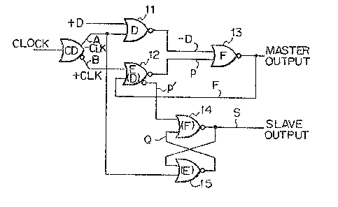
Figu~e 4 is a block diagram of one embodiment of a
master slave latch circuit according to the present
invention. In this embodiment, two of the conventional
latch circuit formed by the NOR gates shown in Fig. lB
ar~ combined, and one gate thereof is commonly used. In
Fig. 4, 11, 12, and 13 form a gate of the master latch
circuit (wherein 12 and 13 are formed as a flip-flop),
and 12, 14, and 15 form a ga~e of the slave latch
circuit (wherein 14 and 15 are formed as a flip-flop~.
As shown in Fig. 4, the gate 12 is formed as a dual NOR
output circuit and i5 commonly used by the màs~er latch
circuit and the slave latch circuit.
That i5, the gate 12 operates as a flip-flop gate
for the master latch circuit, and as a data gate for the
slave latch circuit.
Figure 5 is a block diagram of a second embodiment
of the master slave latch circuit according to the
present invention. In this embodiment, the latch
circuits shown i~ Fig. lA and Fig. lB are combined and
20 one gate is used in common. In Fig. 5, 16, 17, and 18
form a gate of the master latch cixcuit (wherein 17
and 18 are formed as a flip-flop), and 17, 19 and 20
form a gate of the slave latch circuit (wherein 19, 20
are formed as a flip-flop). As shown in Fig. 5, the
gate 17 is commonly used by the master latch circuit and
the slave latch circuit.
In this construction, when the signal is applied
via the gate 12 of the master latch circuit to the gate
of the slave latch circuit (see Fig. 4), and similarly,
via the gate 17 to the gate 19 of the slave latch
circui~ (see Fig. 5), then theoretically, racing can not
occur~ Further, as one gate 12 is commonly used, o~ly
one clock driver i9 used, and thus the da-ta gate ex-
clusively used for the slave latch circuit can be
omitted, which considerably reduces the number of gates.
Figure 6 shows a time chart o the master slave
circuit shown in Fig. 4. In Fig. 6, "~D" is a data
-
-- 7
signal, A is an output line A signal t-CLK) from a clock
driver CD, B is an output line B signal (+CLK) from the
clock driver CD, -D is a signal from the output line -D,
F is an output (master) signal from the gate 13~ P' is
an output of the gate 12 and an input signal of the
gate 14, and S is a slave output signal.
Figure 7 is a concrete example of the circuit of
the gate 12 commonly used by the master and slave latch
circuits. The symbols in Fig. 7 correspond to those
used in Fig. 4. In FigO 7I Ql is a transistor for
inputting the clock signal ~+CLK), Q~ is a transistor
for inputting the mas~er output signal, Q3 is a tran-
~istor for inputting a reference voltagel and Q~ and Q5
are emitter follower transistors for taking out the
lS output.
Here, to avoid mulfunction of the slave latch
circuit in such a master slave latch circuit, the signal
transmission speed of the clock ~ +CLK ~ P' must be
slower than the signal transmission speed of the
clock ~ -CLK -~ P. This can be achieved by providing a
skew in the ~CLK signal or slowing the fall of P'. To
delay the fall of P', it is necessary ~o make the
emitter follower resistance of the transistor Q5 larger
than the emitter ~ollower resistance of the tran-
sistor Q4 or to add the capacitor to the output of thetransistor Q5. Alternatively, a delay gate may be
inserted a~ P'.
~ Figure 8 shows a concrete exampl~ or the circllits
of the commonly used gate 17 in the master slave latch
circuit shown in Fiq. 5 and a gate 16 adjacen~ to the
gate 17. The circuit of the gate 17 is on the left in
~- the figure and the circuit of the gate 16 is on the
right. The connecting portion between the gates 16
and 17 is a circuit of the gate 18.
Figure 9 is a block circuit diagram of a third
embodiment of the present invention. In Fig. 9, 30 is a
cl~ck driver, 31, 32, and 33 are gates orming a master
'
" ' '
.
.
'
~75~3
Iatch circuit, and 3~, 34 and 35 are gates forming a
slave latch circuit. In this embodiment, 32 is the gate
used in common.
The embodiment shown in Fig. 9 is a modification of
the embodiment shown in Fig. 5. In this embodiment,
control signals CMTl and CNT2 are added to the clock
driver, two wires of the input data line are connected
to the data gate of the master latch circuit. In this
construction, the inverted output signal Q of the master
and slave is also output. In Fig. 9, reference numer-
al 91 designates a wired OR (emitter OR) circuit.
Figure 10 i5 a block circuit diagram of a fourth
embodiment of the present invention. In Fig. 10, 40 is
a clock driver, 41, 42, and 43 are gates forming a
15 master latch circuit, 42, 44, and 45 axe gates forming a
slave latch circuit, and 46 and 47 are gates which are
added when necessary, i.e., ~f the input data is in-
crPased. In this embodiment, 42 is the gate used in
common, and 92, 93, and 94 are wired OR circuits.
Figure 11 is a block circuit diagram of a fifth
embodiment of the present invention. In Fig. 11, 50 is
a clock driver, 51, 52, and 53 are gates forming a
master latch circuit, 52, 54, and 55 are gates forming a
slave latch circuit, and 56 and 57 are gates which are
added when necessary, i.e., îf the input data is in
creased. In this embodimentt 52 is the gate used in
common, and 95 and 96 are wired OR circuits.
The embodiment shown in Fig~ 11 is a slight modifi-
cation of the embodiment shown in Fig. 4.
Figure 12 is a block circuit diagram of a sixth
embodiment of the present invention. In Fig. 12, 60 is
a clock dri~er, 61, 62, and 63 are gates forming a
master latch circuit, and 62, 64, and 65 are gates
forming a slave latch circui*. In this embodiment~ ~2
is the gate used in commo~ and 97 is a wired OR cir-
cuit.
The embodimen~ shown in Fig. 12 is similar to the
embodiments shown in Fig. 5 and Fig. 9, but differs
there~rom in that the clock input oE the latch gate 64
of the sla~e latch ~ircuit is i~troduced from an input
side of the clock driver 60.
Figure 13 is a block circuit diagram of a se~enth
embodiment of the present invention. In Fig. 13, 70 is
a clock driver, 71, 72? and 73 are gates forming a
master latch circuit, 72, 74 and 75 are gates forminy a
slave latch circuit, and 76 and 77 are gates which are
added when necessaryJ i.e., if the input data is in-
creased. In this embodiment, 72 is the gate used in
common, and 98r 99, 100 are wired OR circuits.
The embodiment shown in Fig. 13 is similar to the
embodiment shown in FigO 10, but differs therefrom in
that the clock irlput of the latch gate 74 of the slave
latch is introduced from an input side of the clock
driver 70O
Fiyure 14 is a circuit block diagram of an eighth
embodiment of the present invention. In Fig. 14, 80 is
20 a clock dri~er, 81~ 82, and 83 are gates forming a
master latch circuit, 82, 84, and 85 are gates forming a
slave latch circuit, and 86 and 87 are gates which are
added when necessary, i.e., if the input data is in-
creased. In this embodiment, 82 is the gate used in
25 common, and 101, 102 are wired OR circuits.
The embodiment shown in Fig. 14 is similar to the
embodim2nt shown in Fig. 4 and Fig. 11, but differs
therefrom in that the clock input of the latch gate a4
of the slave latch is introduced from an input side of
the clock driver 80.
Figure 15 is a diagram for explaini~g an example of
the operation of the clock driver CD shown in Fig. 4, 5,
9, 10, and 11. In Fig. 15, CLK is an input clock
signal, SM is a sample signal, HD is a hold signal, tG
is a delay per one gate stag~, and ts is a skew value.
In this example, the values of tG ~ tS for each rise and
fall may be different.
, ,
- 10 -
Figure 16 is a diagram Eor e~plaining an example of
the operation of the clock driver CD' shown in FigsO 12,
13, and 14. The same elements as shown in Fig. 15 are
gi~en the same symbolsO In the construction shown in
FigsO 12 and 13, and 14, the clock driver CD may be used
instead of the clock driver CD' shown in Fig. 16.
Further, when the clock driver shown in Fig. 1~ is used
in the construction shown in Figs. 12, 13 and 14, a time
required for one stage of the clock driver can be used
instead of the skew value at the front edge of the clock
driver, and the speed of the master latch is improved by
the skew time o at the front edge of the signal.
Figure 17 i5 a diagram showing an example of the
clock driver CD, and Fig. 18 is a diagram showing an
lS example of the waveforms in the clock driver CD. In
Fig. 17, when the resistors RCSl, RCS2 are not add~d,
the sample signal SM and the hold signal ~D are varied
as shown by broken lines in Fig. 18. When the resis-
tors RCSlo SCS2 are added, the sample signal SM and the
hold signal HD are varied as shown by the solid line in
Fig. 18, in such a manner that the low level side has a
deep fall. This is because the current from the differ-
ential transistor is a constant current, and thus a
superfluous voltage drop is generated by an amount due
to adding the resistors, and this result appears in ~he
sample signal SM and the hold signal HD. Accordingly,
the rise of the waveform of both the SM and the HD signal
is delayed, and thus the skew time t~ is obtained.
When the rise of the SM signal alone is delayed, as
shown in Fig. 16, the resistor RCSl in the circuit shown
in Fig. 17 may be omitted.
As understood from the above description and
accompanying drawings of the embodiment, according to
the present invention, racing can be avoided and the
number of gates can be reduced, and therefore the
advantage of an increase in ~he density of the circuit
can be obtained.
: ' . ' , : ,
: