Note: Descriptions are shown in the official language in which they were submitted.
~ ~s ;3~
IMPROVED PHOTOVOLTAIC HETEROJUNCTION
STRUCTURES
Background
Photovoltaic technology offers great potential as an
alternative source of electrical energy. That potential has not
yet been realized because of the difficulty in making
photovoltaic devices that efficiently transform light, such as
sunlight, into electricity at a cost that is competitive with
conventional energy sources where they are available.
Accordingly, researchers are continually striving to improve the
efficiency of photovoltaic structures.
With respect to junction photovoltaic devices prepared
from semicondllctor materials, various approaches have been taken
to improve efficiency. For example, photoYoltaic structures
including several cells connected in series both electrically and
optically, with respect to incident light, yield improved
efficiency, but at a higher cost of production.
Certain idealized semiconductor structures have been
proposed based on particular theoretical energy band
configurations that would produce improved efficiency. However,
selecting materials that can produce the desired energy band
configurations and actually making examples of the idealized
structures are problems that have not been solved before. One
such theoretical band configuration employs a three layer
structure having a wide bandgap energy window layer for passing
light without significant loss. The next lower layer, lower with
respect to the direction of light incidence, employs a different
material having an optical bandgap energy selected to maximize
absorption from the spectrum of incident light. A final, still
lower or deeper layer, of the same conductivity type as the
middle layer, but formed of a different material, acts to aid
collection of majority charge carriers, but impede the collection
of minority carriers. This heterojunction between the middle and
deepest layer is sometimes referred to as a minority carrier
mirror since it, in effect, reflects minority carriers.
JAW P 1563 1 ~L75 3~6
The promise o the idealized three layer structure
described has not been previously realized. The number of
availahle semiconductor materials from which to select is
limited. The deposition processes for the available materials
considered to date to produce the desired energy band
configuration usually result in the creation of deleterious
interfaces between the different materials.
Summary Of The Invention
In the invention, polycrystalline semiconductor materials
are used to produce a structure having the desired energy band
configuration and improved efficiency performance. Embodiments
of the improved structure have been prepared by employing
electrodeposition technology and show the desired improvement in
performance.
The desired energy band configuration is achieved
according to the invention in a three layer polycrystalline
structure, each layer being composed of a different semiconductor
compound. Two adjacent touching layers are of the same
conductivity type and the other layer is of the opposite
conductivi~y type. At least two of the layers contain cadmium
and at least two of the layers contain tellurium as a principal
constituent of thé compound. The compounds form heterojunctions
at the junctions between the layers. The relatively wide optical
bandgap energy material is advantageously n-type cadmium sulfide
or n-type cadmium sulfide containing zinc in place of some of the
cadmium. The middle layer in which most of the absorption of
light energy occurs to produce charge carriers is advantageously
chosen to be n- or p-type cadmium telluride, cadmium telluride in
which some of the cadmium is replaced by one of the mercury and
zinc or zinc telluride in which some of the zinc is replaced by
mercury. The deepest layer of the novel structures may be p-type
cadmium telluride in which none, some or all of the cadmium atoms
are replaced by zinc or in which some of the cadmium atoms are
replaced by mercury or manganese, provided that the compositions
of the middle and deepest layers are different. Where there is a
JAW-P-1563 3 ,~ S3~L6
substitution of a different element for some of the cadmium atoms
in any of the layers, but particularly in the middle layer, the
amount of that substltution may vary along a line passing ~hrough
the layer and connecting the heterojunctions. This concentration
gradient may improve charge carrier collection efficiency, and/or
the ~hermal expansion coefficient and/or cryskalline lattice
match between adjacent layers. Light conversion efficiency in
excess of 9 percent has been achieved in a structure prepared
according to the invention from electrodeposited layers of
cadmium sulfide, mercury cadmium telluride and cadmium telluride.
Brief Description of the Drawings
Figure 1 is a diagram of an idealized configuration of
energy band edges of an improved photovoltaic structure.
Figure 2 is a diagram of another idealized configuration
of energy band edges of an improved photovoltaic structure.
Figure 3 is a cross sectional schematic view of an
embodiment of a device according to the invention.
Figure 4 is a plot of measured performance results for a
photovoltaic device including a structure in accordance with the
invention.
Detailed Descriptions of
Preferred Embodiments
It is known in the art of semiconductor photovoltaic
devices that multiple layer cells arranged in series optically
provide certain advantages. The layers are referred to as in
series optically because incident light enters one of the layers
and after passing through that layer enters the next layer, etc.,
until it has passed through all the layers or is entirely
absorbed. The top layer, i.e. the layer that first receives
incident light, preferably has a wide optical bandgap energy so
that little of the incoming light from the sun or another light
:. ' - '- . :
JAW-P-1563 fi ~753~
source is absorbed in that layer. For passage of sunlight, it is
desired that the optical bandgap energy of the first layer be
relatively large, perhaps 2.0 electron-volts (ev) or more. The
top layer functions as an electrical contact for collecting light
generated charge carriers. The next deeper layer, deeper with
respect to the direction of travel of light, has a smaller
optical bandgap energy, preferably one that is selected to
optimize absorption of the incident light considering its
spectral distribution. Most of the incident light is absorbed in
that layer and generates electronic charge carrier pairs that are
collected at the terminals of the device as the photovoltaic
current. For the solar spectrum, an ideal optical bandgap energy
for the middle layer is about 1.4 to 1.5 eV. If the three layer
structure is used as a unit cell in a cascade structure
incorporating several unit photovoltaic cells arranged in series
optically, then the bandgap energies of the middle layers of each
of the unit cells should be different, with the narrowest bandgap
energy material being disposed in the deepest cell. Since in the
unit cell the optical bandgap energies of the top and middle
layers are different, it is obvious that the layers in the
desired structure are each formed of different materials.
Therefore, their interfaces are heterojunctions. Likewise, it is
obvious that for the three layer structure being described, it is
necessary that the top and middle layer form a rectifying
junction, i.e. be of opposite conductivity types, in order to
achieve acceptable photovoltaic performance.
The deepest layer preferably forms with the middle layer a
minority charge carrier mirror. The minority carrier mirror
"reflects" minority carriers back toward the middle layer, but
encoura~es collection of majority carriers. The effect is to
reduce the diode saturation current, enhancing the open circuit
voltage and, thereby, the efficiency of a photovoltaic cell.
Such charge carrier mirrors are known in the art and are achieved
by making thè conductivity types of the middle and deepest layer
the same and more strongly doping the deepest layer relative to
the doping level of the middle layer. Use of a heterojunction at
..
JAW- P- 1 5 6 3 5 ~L~7~3~ ~
the junction of the middle and deepest layers is an alternative
and supplementary method of realiæing a minority carrier mirror.
An energy band edge diagram of the three layer structure
just described, i.e. with three layers disposed in sequential
touching contact and optically in series, is shown in Figure 1.
There, the conventional Fermi level, EF, is shown at equilibrium
as a constant energy level throughout the three regions of the
structure. In accordance with the usual convention, the
conduction band edge, Ec, is shown disposed abo~e the Fermi level
and the valence band edge, Æv, is shown below the Fermi level.
In region 1, i.e. the top layer, the wide optical bandgap energy
material is shown as n-type material, i.e. a material in which
electrons are the majority charge carriers. In region 3, i.e.,
the middle layer, a relatively narrow gap p~type material is
shown. The band edges between regions 1 and 3 are oblique
because the transition in conductivity types between the regions
forms a space charge region. The space charge region sweeps
charge carriers generated by absorbed light toward the terminals
of the structure aiding their collection.
In addition, there is a discontinuity in the valence band
edga because of the heterojunction, i.e. the narrowing of bandgap
energies as the depth of light penetration in the cell increases.
The discontinuity occurs in the valence band edge by judicious
choice of the materials forming regions 1 and 3, bearing in mind
their respective electron affinities. Preferably the electron
affinity of the material in region 1 should be greater than that
o the material in region 3. However, the electron affinity of
the material of region 1 can be smaller than that of region 3,
but not more than abou~ 0.1 eV smaller. ~ccording to the rule
commonly applied, the difference in the electron affinities of
the two materials equals the discontinuity in the valence band
edges between the region 1 and 3. However, it is also recognized
that that rule ls not always applicable.
In region 5, the deepest layer of the structure with
respect to the direction of light penetration, is another p-type
JAW-P-1563 6 ~L~7~;33..6
material that is of wider bandgap energy. Preferably, the Fermi
level in region 5 is closer to the valence band edge than in
region 3. The material in region 5 has a smaller electron
affinity than the material in region 3, accounting for the
discontinuity the conduction band edge. It is this discontinuity
that acts as a minority charge carrier mirror.
Constructing a three layer structure having an energy band
configuration like the ideali2ed diagram shown in Figure 1
requires numerous practical considerations. Layers 1 and 3 and
layers 3 and 5 should preferably have nearly the same thermal
coefficients of expansion and lattice constants (assuming ordered
and not amorphous materials are used). ~or example, in the case
of a lattice constant mismatch, interface states can be created
at the heterojunction that adversely affect the performance
characteristics of the structure. An undesirably high
concentration of interface states can result in excessive charge
carrier recombination, severely reducing collected current. When
materials containing at least three principal constituents (i.e.
elements that are present in amounts to form a significant part
of the atomic lattice and not in relatively small quantities as
dopants or trace contaminants) are used in a layer, the relative
amounts of two of the constituents can vary with position ln one
of the layers, such as the middle layer. An example is
illustrated in Figure 2, where the middle layer has an optical
bandgap energy that varies with position along the direction of a
line connecting the two heterojunctions. As a result of that
variation, at least one band edge is tilted and therefore aids
collection of charge carriers. The compositional variation can
also reduce the effects of mismatches in thermal expansion
coefficients and/or in lattice constants.
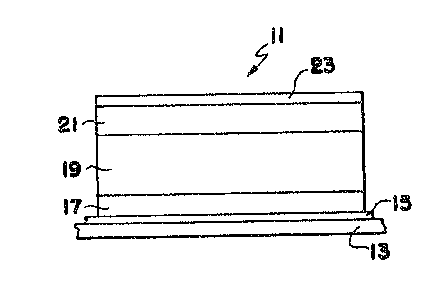
The structure described needs additional physical elements
to function as a photovoltaic cell. An example of a completed
unitary cell device 11 incorporating the structure is shown in
Figure 3. ~evice 11 includes a substrate 13 on which, if
necessary, an electrically conducting layer 15 is disposed. The
three layers 17, 19 and 21 of the novel structure are disposed on
.
.
. ~ ~
JAW-P-1563 7 ~ ~7~3~
conductive layer 15 and a second conductive layer 23 is disposed
on layer 21. Substrate 13 may be transparent~ such as glass, or
may be opaque In the former case, light passes through the
substrate into layer 17 which may be the top cell of the
structure. A transparent dielectric substrate 13 requires a
transparent, electrically conducting layer 15 to form one
terminal of device 11. Appropriate conducting layers can be made
from tin oxide, indium tin oxide, zinc oxide and other
transparent, electrically conducting oxides as is well known in
the art. In an inverted form of device 11, layer 21 may be the
top layer in which case layer 23 may be transparent, as well as
electrically conductive, and may be in the form of or include a
current collecting grid. In this case, substrate 13 may be
opaque and electrically conducting, meaning that layer 15 may be
unnecessary.
The problem in realizing the idealized three layer
structure described is the selection of available semiconductor
materials that have the characteristics described and can be
united in the structure without loss of per~ormance. sy means of
the invention, the structure can be realized using
polycrystalline semiconductor materials. The so-called II-V
polycrystalline semiconductors (referring to the IIs and VIA
columns of the Periodic Table of Elements as published by the
American Chemical Society) that can be prepared by
electrodeposition can be used to construct the structure and
achieve the performance that previously has only been discussed
theoretically.
An appropriate material for the "topl', i.e. window, layer
of a structure according to the invention is cadmium sulfide
which has an optical bandgap energy greater than 2 eV. Cadmium
sulfide can be deposited by numerous methods including
electrodeposition and p.lasma spraying. Cadmium sulfide can be
modified by substituting zinc for some of the cadmium atoms, i.e.
to form CdyZn1_yS, where y ranges from more than zero to no more
than one, resulting in an increase in optical bandgap energy with
~2~5~
JAW-P-1563 8
increasing zinc. These materials generally exhibit n-t~pe
conductivity.
In a unit ce~l, as shown in Figure 3, when cadmium
sulfide is used as the top layer, zinc oxide can be used
advantageou.sly as the electrically conductive transparent ~ilm
15. It is desirable that the cadmium sul~ide layer be as thin
as possible to minimi~e the amount of light absorbed in the
top layer and be heavily doped to minimize ohmic losses.
However, a charge depletion region is formed at the junction
of the top and middle layers of the cell when those layers are
of opposite conductivity types. If the cadmium sulfide layer
is ~ery thin and not too heavily doped, the depletion layer
can extend almost all the way through the cadmium sulfide
layer. However, because zinc oxide has a different electron
affinity from that of tin oxide/ with or without indium, its
use is preferred since with it a thinner cadmium sulfide layer
may be used.
Cadmium telluride alone and with the substitution by
one of mercury and zinc for some of the cadmium atoms and
mercury zinc telluride are appropriate materials for the
middle or photovoltaic layar of the structure in which most of
the light is absorbed. The optical bandgap energ~ of cadmium
telluride is about 1.5 e~ which is nearly ideal for absorption
of light from the solar spectrum. Cadmium telluride may be
electrodeposited on a conducting substrate, such as on a layer
of cadmium sulfide, using known technology. See U.S. patents
4,388,483, to Basol et al., 4,400,2~4 to Kroger et al. and
4,425,194 to Kroger et alO Inclusion of mercury in place of
some of the cadmium can reduce the optical bandgap energy of
cadmium telluride to an even more optimal value for light
absorption from the solar spectrum. ~ method for
electrodepositin~ mercury cadmium talluride, CdxHg1xTe where x
ranges from more than zero to less than one, is disclosed in
U.S. patent 4,548,681 to Basol et alO Similarly CdxZnlxTe and
HgxZn1xTe where x ranges from more than zero to less than one,
are suita~le for use in the photovoltaic layer. CdxZnlxTe and
JAW-P-1563 9
S3~i
HgxZnl_xTe can be electrodeposited yenerally following the
techniques disclosed in the Kroger and ~asol patents. The ions
in the electroplating bath must be changed and the plating
potentials must be adjusted because of the different quasi-rest
potentials of zinc and mercury compared to that of cadmium.
These middle layer materials are generally n-type when
electrodeposited. However, if heat treated for sufficient time
at a high enou~h temperature, as described in U.S. patents
4,388,483 and 4,548,681, for CdTe and CdHgTe, these materials can
be converted to p-type conductivity.
The deepest layer of the structure can be formed of
cadmium telluride, zinc telluride (generally Cd~Zn1_zTe),
CdzHgl~zTe or CdzMnl_zTe where z is more than zero and no more
than one. The appropriate material depends on the material used
in the middle, photovoltaic layer. The energy bandgap of zinc
telluride is about 2.3 eV and it forms a continuous series of
compounds with cadmium telluride. 17 Sov. Phys. Semiconductors,
#5, pp. 585-86 (1983). Therefore, by adjusting the ratio of zinc
to cadmium, an optical bandgap energy greater than that of
cadmium telluride can be achieved. Of course, if the bandgap
energy of the light-absorbing material in the middle layer is
less than that of cadmium telluride, as is the case with mercury
cadmium telluride, then the deepest layer of the structure can be
cadmium telluride. Zinc telluride characteristically exhibits p-
type conductivity and, as previously explained, electrodeposited
cadmium telluride usually has n-type conductivity, but can be
converted to p-type conductivity with a heat treatment.
Electrodeposition is a particularly advantageous method of
preparing structures according to the invention.
Electrodeposition processes are carried out at temperatures of no
more than about 100C~ Preferably, a deposited layer is very
quickly transferred from one electrodeposition bath to another
for growing the next layer. The very limited exposure time
between the deposition of different layers and the relatively low
temperatures used, discourage the formation of oxides or other
interfacial layers that could adversely afect ~he performance of
- - ' ~ ''
~- . .: '
,
' ' '
JAW-P-1563 ~ ~ ~53~
the resulting structure. Any heat treatment step for
conductivity type conversion of any of the layers is preferably
carried out after all layers are deposited rather than between
deposition of different layers. Other low temperature deposition
processes are also expected to produce structures according to
the invention having good pe~formance characteristics.
Particularly appropriate combinations of materials for the
layers of the novel polycrystalline photovoltaic structure are
listed in Table I.
Table I
Examples of Structures In Accordance With the Invention
Example Layer A Middle Layer Layer B
1 n CdS p CdxHgl-xTe p CdTe
2 n CdS p CdxHg1_xTe p ~dzHgl-zTe
3 n CdS n CdTe p ZnTe
4 n CdS p CdTe p CdzZnl_zTe
n CdyZn1_yS P CdxZn1_xTe p CdzZnl_zTe
6 n CdyZn1_yS P CdxHg1_xTe p CdzZnl_zTe
7 .n Cd5 p CdTe p CdzMnl_zTe
8 n CdS p Hgxznl-xTe p CdTe
Thus it is noted that the preferred polycrystalline
semiconductor materlals employed in these structures include
cadmium as a principal constituent in at least two and,
frequently, all three of the layers. Likewise, sulfur is always
present as a principal constituent in one of the layers.
Tellurium is present as a principal constituent in two of the
layers. Selenium is never intentionally present in any of the
layers. Selenium can migrate during deposition processes and
during heat treatment of layers, creating unwanted interfaces or
junctions that adversely affect performance of the structure.
Structures having middle layers including three chemical
elements can have the graded energy band structure of Figure 2.
, ~, , : .
:: '
' .
'~ ' '
JAW-P-1563 11
~753~
The grading is accomplishing by varylng the relative quantities
of the two group II elements that are present in the layer, e.g.
Cd and H~ Cd and Zn, along a line passiny through the middle
layes and connecting the two heterojunctions. With respect to
~xa~ples 2 and 5, z must be greater than x or the minority
carrier mirror will not be formed.
Example 3 in Table I is a somewhat different structure
from the other examples. In Examples 1, 2 and 4-8, layer A is
the window layer through which light first enters the structure.
This arrangement is apparent since in those examples the window
layer and the light-absorbing layer are of opposite conductivity
types. In the desired structure, the light-absorbing layer and
layer that form the minority carrier mirror are of the same
conductivity type. In Example 3, the same conductivity type
layers are layer A and the middle layer. In the other examples,
the same conductivity type layers are the middle layer and layer
C. That is, Example 3 is an "upside down" structure relative to
the other examples. It can he formed on an opaque substrate
assuming, as is conventional, that the cadmium sulfide layer is
deposited ~irst. A molybdenum substrate or thin layer of
molybdenum disposed on another substrate is an appropriate base
for a photovoltaic cell usiny the structure of Example 3. The
middle layer is kept n-type by avoiding any processing steps at
temperatures sufficiently elevated to convert the conductivity
type of the cadmium telluride middle layer. With the other
examples of Table I, it is contemplated that glass or another
transparent substrate bearing a transparent, electrically
conductive layer, if necessary, will be used with the structures
in photovoltaic cells. In that case, the layers will be usually
be deposited in the sequence of layer A, middle layer and layer B
sequence.
Figure 4 displays the measured performance characteristics
of a photovoltaic device having a single cell constructed of the
materials of ~he Example 1 type from Table I. The electrical
contacts forming the electrical terminals of the devices were
indium tin oxide contacting the cadmium sulfide and gold
.
", ~
,,
JAW-P-1563 12
~ ~753~
contacting the cadmium telluride. This heterojunction cell hss
the characterlstics llsted in Table II. The efficiencies of
cells according to the invention have shown about 10~ improvement
in efficiency compared to similar cells without a minority
carrier mirror. The efficiency improvement is largely
attributable to increases in open circuit voltage and, to a
lesser degree, improvements in fill factor.
Table II
Measured Characteristics of an Embodiment of a
Photovoltaic Cell In Accordance with The Invention
Figure 4
Efficiency (percent) 9.7
Open circuit voltage !volts) 64
Short circuit current (mA) 1.8
Fill factor 0.53
The foregoing description concerns a three layer
photovoltaic structure that can be part of a photovoltaic device.
One such structure may be incorporated in a single cell
photovoltaic device or several of the three layer structures may
be included in a multiple cell, cascade device with the cells
arranged in optical series and, perhaps, connected in series
electrically.
The invention has been described with respect to certain
preferred embodiments. Various modifications and additions
within the spirit of the invention will occur to those of skill
in the art. Accordingly, the scope of the invention is limited
solely by the following claims.
', , ' ' . . , :
:, :
..
,