Note: Descriptions are shown in the official language in which they were submitted.
1;275~456
BACKGROUND OF THE INVENTION
This invention relates generally to latch-up protection
circuitry for integrated circuits using complementary MOS circuit
technology and, in particular, to latch-up protection circuitry
which largely voids occurrence of latch-up effects.
In general, integrated circuits which use complementary
MOS technology have a semiconductor substrate which does not lie
at the ground potential of the integrated circuit, but is
negatively charqed by a substrate bias generator. ~t is known
that biasing a semiconductor substrate reduces the transistor and
barrier layer capacitances and improves the switching speed of
the integrated circuit. For example, for a semiconductor
substrate of p-conductive material having inserted therein
n-conductive, well-shaped semiconductor zones, the substrate is
typically negatively biased in the range -2 to -3 volts. The
~ource regions of field effect transistors that are provided on
the semiconductor substrate and which are outside of the well-
shaped semiconductor zone are connected to a ground potential,
since the semiconductor substrate has a negative bias.
When a positive supply voltage for the integrated
circuit is switched on, the p-conductive semiconductor substrate
is initially in a condition of nfloating'l, that is, it is not
connected to any external potentials.
This floating condition terminates when the substrate
biased generator takes effect. The time span between the turn on
of the positive supply voltagè and the activation of the
substrate bias genexator is essentially influenced by such
factors as clock frequency, existing coupling capacitances and
existing capacitive load. During the time of "floating", t~he
semiconductor substrate can be temporarily charged to a positive
~.Z~54~
bias via the barrier layer capacitances which are present, first,
between the well-shaped semiconductor zone and the substrate and,
second, bet~een the substrate and the source regions of the field
effect transistors which axe connected to ground potential. This
initial positive bias is not removed until the substrate bias
generator takes effect, that is, until the negative substrate
bias gradually builds up at the output of the substrate bias
~enerator. Even during operation of the integrated circuit, high
currents that are diverted from the semiconductor substrate via
the substrate bias generator to a terminal of the substrate lying
at ground potential can lead to a positive bias of the
semiconductor substrate. This is due to voltage drop off at the
internal resistor of the substrate bias generator. Positive
biases, however, represent a high safety risk for the integrated
circuit since a latch-up effect can be triggered thereby
disabling the integrated circuit.
For a clearer understanding of the latch-up effect, it
can be assumed that four successive semiconductor layers of
alternating ccnductivity types are ~enerally present between a
terminal of a field effect transistor of a first channel type
lying in the well-shaped semiconductor zone and a terminal of a
field effect transistor Gf a second channel type located outside
of this zone on the semiconductor substrate. The terminal of the
former transistor forms the first semiconductor layer, the well-
shaped semiconductor zone forms the second, the semiconductor
substrate forms the third, and the terminal of the latter
transistor forms the fourth semiconductor layer. As a
consequence of this structure, a parasitic bipolar pnp transistor
and an npn transistor are created. The collector of the pnp
transistor corresponds to the base of the npn transistor, and the
1 2~S45~
base of the pnp transistor corresponds to the collector of the
npn transistor. This structure forms a four layer pnpn diode, as
is typicall~ found in a thyristor. When the semiconductor
substrate has a positive bias, the pn junction between the third
and fourth semiconductor layers can be biased such that a current
flow occurs between the latter transistor terminals, this current
path to be attributed to a parasitic thyristor effect within the
four layer structure. The current path then continues to exist
even after the positive bias is removed from the substrate and
this current path can thermally overload the integrated circuit.
For reducing the transistor and barrier layer
capacitances, it is known to use a negative substrate bias in
NMOS technology, which is generated by a substrate bias generator
on the integrated circuit (Ralbleiter Elektronik, 14, H. ~eiss,
K. Horninger, "Integrierte MOS-Schaltungen", pp. 247-248). The
latch-up effect resulting from positive semiconductor substrate
biases is also described in this reference on pages 111 through
112. The proposed solution to the latch-up problem presented in
this reference is a modification of the doping profiles in the
design of the semiconductor wells. Another proposed solution for
suppressing the latch-up effect is presented in the publication
of D. Takacs et al, 7'Static and Transient Latch-Up Hardness in n-
well CMOS With On-chip Substrate Bias Generator", IEDM 85,
Technical Digest, pp. 504-508. This reference discloses a
clamping circuit which prevents the latch-up effect in that the
semiconductor substrate potential is limited to a value which is
not sufficient for activating the parasitic bipolar transistors
in the semiconductor substrate. To accomplish this, the clamping
circuit diverts the high capacitance charging currents to grsund.
~ ~5~56
However, the prior art clamping circuit does not
fundamentally exclude the possibility of a positive charging of
the semiconductor substrate, rather the effects of latch-up are
merely compensated in that, should a positive charging of the
semiconductor substrate occur, a low impedance connection to
ground is utilized to eliminate the positive charging.
The present invention overcomes these drawbacks in the
prior art and in a circuit embodying the present invention the
occurrences of latch-up effects are largely avoided.
SUMMARY OF THE INVENTION
The present invention is a novel latch-up protection
circuit for use in integrated circuits using complementary MOS
circuit technology. The integrated circuit has a substrate bias
terminal in a doped semiconductor substrate. The substrate bias
terminal is connected to an output of a substrate bias
generator. A capacitor has a first surface which is integrated
in the doped semiconductor substrate. An electronic protection
circuit is connected to and is responsive to a voltage on the
substrate bias terminal. The electronic protection circuit is
connected to a second surface of the capacitor and has at least
one first transistor with a predetermined threshold voltage. A
capacitor bias generator provides a prede~ermined voltage and is
connected to the electronic protection circuit. The electronic
protection circuit disconnects the capacitor bias generator from
the second surface of the capacitor when a voltage on the
substrate bias terminal is greater than a difference between a
reference potential and the threshold voltage of the first
transistor in the electronic protection circuit. SimilarlyJ the
electronic protection circuit connects the capacitor bias
~.275455
generator to the second surface of ~he capacitor when a voltage
on the substrate bias terminal is lower than the difference.
The electronic protection circuit has a comparator for
comparing the voltage on the substrate bias terminal to the
difference defined above. Also, the circuit has an amplifier
connected to the comparator which in turn is connected to an
electronic switch such that the switch is controlled by the
output of the amplifier and connects or disconnects the second
surface of the capacitor and the capacitor bias generator.
The present invention has the advantage that the
undersirable high charging currents of the semiconductor
substrate which can trigger a latch-up effect are eliminated in a
straightforward and simple manner.
BRIEF DESCRIPTION OF THE DRAWINGS
Features of the present invention which are believed to
be novel as set forth with particularity in the appended
claims. The invention, together with further objects and
advantages, may best be understood by reference to the following
description, taken in conjunction with the accompanying drawings,
and the several flgures of which like reference numerals identify
like elements, and in which:
FIG. 1 is a schematic view depicting an integrated
circuit having a one transistor memory cell and using latch-up
protection circuitry of the present invention;
FIG. 2 is a schematic illustration of the FIG. 1
integrated circuit with the addition of a clamping circuit;
FIG. 3 is a general block diagram of the latch-up
protection circuit used in FIGS. 1 and 2;
FIG. 4 is a schematic diagram of the FIG. 3 latch-up
protection circuit using an ohmic load;
S4~i5
FIGS. 5 and 6 are schematic diagrams of alternative
embodiment of the FIG. 3 latch-up protection circuits using
capacitive loads; and
FIG. 7 is a schematic diagram of an implementation of an
electronic switch used in the FIG. 3 latch-up protection circuit.
DESCRIPTION OF THE PREFERRED EMBODIMENT
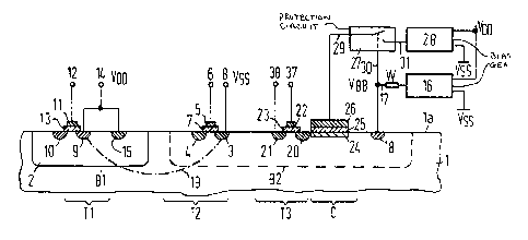
The present invention has general applicability but is
most advantageously used in an integrated circuit of the type
shown in FIG. 1. The FIG. 1 integrated circuit utilizes the
latch-up protection circuit of the present invention which is
constructed on a semiconductor substrate 1 of doped semiconductor
material, for example, p-conductive silicon. The semiconductor
substrate 1 has an n-conductive, well-shaped semiconductor zone 2
that extends up toward the boundary surface la of the
semiconductor substrate 1. Also, n+-doped semiconductor regions
3, 4, 20 and 21, which form source and drain regions of two
n-channel field effect transistor~, T2 and T3, are inserted into
the semiconductor substrate at a location outside of the
semiconductor zone 2. In this example, a capacitor C may be
arbitrarily fashioned, but is shown composed of a planar
dielectric layer 25, of a planar polysilicon layer 26 and of a
planar, n-doped layer 24. This capacitor C, together with the
n-channel field effect transistor T3, form a one transistor
memory cell into which information can be written or from which
information can be read o~t. The channel region lying between
regions 3 and 4, and similarly between regions 20 and 21, are
covered by gates 5 and 22, respectively. Gates 5 and 22 are
provided with terminals 6 and 37, respectively, and are separated
on the boundary surface la by thin, electrically insulating layer
7 and 23, respectively, which may be, for example, SiO2. the
~z~s~
drain region 21 is connected to a terminal 38, whereas the source
region 3 is connected to a terminal 8 which is at the ground
potential vss. Further, p -doped regions 9 and 10, ~hich are the
source and drai.n regions of a p-channel field effect transistor
Tl, are inserted into the semiconductor zone 2. The channel
region lying between the regions 9 and lO is covered by a gate ll
which is connected to a terminal 12 and separated from the
boundary layer la by thin, electrically insulating layer 13,
which may also be composed of SiO2. The source region 9 of the
field effect transistor Tl is connected to a terminal 14 which in
turn is connected to a supply voltage VDD. The semiconductor
zone 2 lies at the supply voltage VDD via an n -doped contact
region 15 which is connected with the terminal 14.
A substrate bias generator 16 generates a negative
substrate bias of, for example, -2 to -3 volts, and is also
connected to a reference potential, which is shown as the ground
potential Vss in the present embodiment of FIG. l, and to the
supply voltage VDD. An output 17 of the substrate bias generator
16 is connected to an input 30 of the latch-up protection circuit
27. Also, the output 17 is connected to a p+-doped substrate
voltage terminal 18 that is inserted into the semiconductor
substrate l. Semiconductor substrate l is thus at the negative
substrate bias VBB generated by the substrate bias generator 16,
whereas the source regions, for example, region 3 of the field
effect transistor T2, are connected to the ground potential
Vss. As a result thereof, the barrier layer capacitances of the
drain and ~ource regions of the field effect transistors in the
semiconductor substrate are reduced. In order to avoid a
latch-up effect that might occur along the four layer structure
3, 1, 2 and 9, along the broken liné 19 between the terminals 8
l.Z~ 55
and 14, the electronic protection circuit 27 reduces the
capacitive charging currents of the capacitor C to valuPs which
are insufficient for charging the substrate 1 to such a positive
degree that a latch-up effect i5 triggered. Depending on the
voltage level appearing at the input 30 of the electronic
protection circuit 27, an input 31 may be electrically connected
to an output 39 which in turn i.s connected to capacitor surface
26 of the capacitor C. The input 31 is connected to a capacitor
bias generator 28 that is in turn connected to the referenc~
potential VSs and to the supply voltage VDD. The output voltage
of the capacitor bias generator 28, for example, can amount to
half the supply voltage, that is, it may have a value of up to
VDD/2. The input 30 of the electronic protective circuit 27 is
simultaneously connected to the output 17 of the substrate bias
generator 16 and to the p~-doped substrate bias terminal 18.
Under turn-on conditions of the integrated circuit and where
voltages VBB are higher than an internal reference voltage, for
example, Vss, of the electronic protection circuit 27, the
circuit 27 causes an interruption between the input 31 and the
output 29. Therefore, when the substrate potential approaches a
given positive value, the capacitive charging currents from the
capacitor bias generator 28 into the capacitor C are
suppressed. For example, this may occur when the voltage supply
VDD is switched on and the semiconductor substrate 1 tends to
rise to a positive bias due to the capacitive charging currents
during the time period before the substrate bias generator 16
reaches its full negative bias level. In normal operations, that
is, when tne substrate is negatively biased, the capacitor
surface 27 is connected to the capacitor bias generator 28 in a
low impedance faRhion via the electronic protective circuit 27.
- l.Z75~
FIG. 2 shows a second embodi.ment of the present
invention that differs from FIG. 1 in that an additional clamping
circuit is ~dded to the FIG. 1 embodiment. The output 17 of the
substrate bias generator 16 is connected in FIG. 2 to a circuit
point that is situated at the ground potential V~s. This is
achieved by an electronic switch, field effect transistor T4. In
the illustrated embodiment, the circuit point is terminal 36
which is connected to the reference potential Vss.
More specifically, the output 17 of the substrate bias
generator 16 as shown in FIG. 2 is connected to an n -doped
semiconductor region 32 which ~s inserted into the semiconductor
substrate 1. Another n+-doped semiconductor region 33 in the
semiconductor substrate 1 is connected to terminal 36 which is at
the ground potential Vss. The region of the semiconductor
substrate 1 lying between the regions 3~ and 33 is covered by a
gate 35 that is separated from the boundary surface la by a thin,
electrically insulating layer 34 composed, for example, of
SiO2. Together with the gate structure, 34 and 35, the regions
32 and 33 form the n-channel field effect switching transistor
T4. The drive for transistor T4 is derived from output 17 which
is connected to the gate 35.
The switching trans.istor T4 in FIG. 2 should have a low
threshold voltage which is lower than the forward voltage for the
pn junction between regions 1 and 3. This can be achieved in the
traditional way, for example, the region of the semiconductor
substrate 1 lying between the regions 32 and 33 doe~ not have any
doping in addition to the basic doping which, for example,
amounts to 1015cm 3. The channel regions of the remaining field
effect transistors, for example, T2, are provided with an
additional doping which intensifies the basic doping. This may
_g_
1 2~7~5~
expediently be introduced by way of an implantation with a dose
of about lOl~cm 2. When two different insulating layer
thicknesses are available in the manufacturing technology
employed, then the smaller is expediently used for region 34, for
example, approximately 15 nm, whereas a thickness of about 20
thro~gh 25 nm is selected for the layer 7 and 13. When the
semiconductor substrate 1 is at a positive bias, for example~
during the turn-on period of the supply voltage VDD and when the
substrate bias generator has not yet reached its full negative
voltage level, then the gate 35 is also correspondingly
positively biased. This leads to the fact that the switching
transistor T4 becomes conductive when the low threshold voltage
is exceeded. The voltage at the output 17 of the substrate bias
generator 16 is thus limited to the value of the low threshold
voltage.
Whereas the electronic pro~ective circuit 27 prevents a
positive charging of the semiconductor substrate 1 by
interrupting the capacitive charging current of the capacitor C,
the additional clamping circuit of transistor T4 operates to
prevent all other possibilities of positive substrate charging.
This may occur, for example, when high currents derive during
operation of the integrated circuit. These high currents may
flow to the ground potential Vss via a current path consisting of
the semiconductor substrate l, the terminal 18, the output 17 and
the substrate bias generator 16. When this occurs, then a
voltage drop off can arise at the internal resistor W of the
substrate bias generator 16, thus causing the output 17 and
therefore the semiconductor substrate 1 to receive, at least
temporarily, a positive bias. In this situation, these currents
--10--
~ 275~
are eliminated by the additional clamp~.ng circuit shown as field
effect transistor T4 in FI~. 2.
The substrate bias generator 16, electronic protection
circuit 27, and the capacitor bias generator 2B shown in FIGS. 1
and 2 are expediently co-integrated on the semiconductor
substrate.
FIG. 3 shows a basi.c circuit in general block diagram
form of the electronic protection circuit 27. As shown, th~
circuit has three discrete components, a comparator K having an
input 30, an amplifier V and an electronic switch S which has an
input 31 and an output 29. The comparator R compares the voltage
appearing on input 30 wi~h an in~ernally derived voltage value
or, for example, to the ground potential Vss. When the result of
the comparison is positive, a corresponding signal is sent to an
output 30a. This signal i6 amplified by amplifier V and con~rols
electronic switch S. Electronic switch S connects the input 31
to the output 29 depending upon the results of the comparison
made in the comparator K. When the voltage appearing on input 30
is lower than the internal voltage value, the input 31 and the
output 29 of the electronic switch S are electrically connected
to one another. The amplifier V can be optionally inte~rated
depending on the required matching on the output signal of
comparator K to the electronic switch S.
FIG. 4 shows one embodiment of electronic protective
circuit 27 having an ohmic load. As shown, it is composed of
only two components, a comparator K and an electronic switch S.
A series circuit of an n-channel field effect transistor T5 and
an ohmic load element forms the comparator K. In the present
embodiment, the ohmic loaa element is formed by a p channel field
effect transistor TS whose substrate is connected to its source
--11--
~ ~7S~55
terminal. The gates of the field effect transistors T5 and T6
are interconnected and also connected to the grou~d potential
Vss. One terminal (the source of field effect trar,sistor T6) of
the series circuit on the ohmic load element side is connected to
the supply VDD and the other terminal of the series circuit, that
is, the substrate terminal of the field effect transistor T5 are
connected to the input 30 of the electronic protection circuit
27. The electronic switch S is formed by a p-channel, field
effect transistor T7. Source and drain terminals respectively
form the input 31 and the output 2~ of electronic protection
circuit 27. A junction 39 is the connection of the gate of the
p-channel field effect transistor T7 to the drains of transistors
T5 and T6. The substrate terminal of the field effect transistor
T7 is connected to the supply voltage VDD.
Whether during turn on or during operation of the
integrated circuit, if the voltage at the input 30 exceeds the
reference potential Vss less the threshold voltage, UT, of the
field effect transistor T5, then the output voltage of the
comparator K at the junction 39 rises. The field effect
transistor T5 becomes non-conductive and the junction 39 has a
voltage level equal to the supply voltage VDD through the load
element, that is, the p-channel field effect transistor T6. For
this reason, the p-channel field effect transistor T7 becomes
non-conductive and the connection between th~ input 31 and the
output 29 is interrupted. Given a substrate bias at the input
30, which is lower than the difference tVSs-UT), the field effect
transistors T5 and T7 assume a conductive state, so that the
input 31 and the output 29 are electrically connected to one
another. A 15w forward current will flow through the field
-12-
~.275~56
effect transistors T5 and T6 d~ring operation in accordance with
their parameters.
FIGS. 5 and 6 show two alternative embodiments of an
electronic protection circuit 27 having a capacitive load. They
are similarly composed of two components each, a comparator K and
an electronic switch S. As shown in FIG. 5, the capacitive load
can be formed by a p-channel field effect transistor T9 connected
as a capacitor or, as shown in FIG. 6, can be formed by proper
dimensioning of the gate capacitance of the p-channel field
effect transistor T7. Electronic protection circuit 27 shown in
FIGS. 5 and 6 differ only in the implementation of their
capacitive load elements. The p-channel field effect transistor
T9 utilized for this purpose in FIG. 5 has its source, drai~ and
substrate terminals connected to the supply voltage VDD. The
field effect transistor T9 may be eliminated as shown in FIG. 6
if the parameters of the field effect transistor T7 are properly
established in order to effect the desired gate capacitance.
When the voltage at the input 30 in the FIGS. 5 and 6
embodiments exceeds the voltage Vss-UTl then the n-channel field
effect transistor T5 becomes non-conductive. The voltage level
at the junction 39 is substantially equal to the supply voltage
VDD via the uncharged capacitor. The field effect transistor T7
becomes non-conductive and interrupts the connection between the
input 31 and output 29. When the voltage on the input ~erminal
30 falls beolow the voltage Vs~-UT, then the field effect
transistor T5 becomes conductive and charges the capacitor. The
field effect transistor T7 is likewise placed in a conductive
state and the connection between the input 31 and output 29 is
established. During normal operation, the capacitor of FIG. 5
and the gate capacitance of FIG. 6 are charged and, $herefore,
75~
the electronic protection circuits of FIGS. 5 and fi differ from
that shown in FIG. 4 in that ~hey are free of fcrward currents.
The elec~ronic switches S in FIGS. 4, 5 and 6 where
formed exclusively by p-channel field effect transistors. FIG. 7
shows an alternative embodiment in which the electronic switch s
is replaced by an n-channel field effect transistor T8. This may
be necessary, for example, when an electronic switch having
higher current yield is required. To accomplish this, the
n-channel field effect transistor T8 is preceeded by an inverter
I. The substrate terminal of transistor T8 is connected to the
substrate bias VBB, which appears on the output 17. Source and
drain terminals are connected respectively to the input and
output, 31 and 29. The inverter I is connected to the supply
voltage VDD and the reference potential VSs. An input of the
inverter I is connected to the junction ~9.
In addition to the embodiments described above, the
invention also envisions embodiments wherein an n-conductive
substrate is provided with p-conductive, well-shaped
semiconductor zonesO The conductivity types of all silicone
parts and the polarities of all voltages are replaced by their
respective opposite counterparts.
Furthermore, embodiments derived from those shown in
FIGS. 1 and 2 may be envisioned having the following
modifications. The boundary line Bl may be omitted and the
substrate 1 and the zone 2, may be considered to both be an n-
conductive substrate. Therefore, a p-conductive, well-shaped,
semiconductor zone must then be inserted into t~is n-conductive
substrate. This p-conductive zone is separated from the
n-conductive substrate by the broken line B2 and contains the
circuit elements T2, T3, C, T4 and terminal 18.
-14-
i456
A preferred application of the present invention is
utilized in circuits of dynamic semiconductor memories having
high packing density. These periphery circuits are
monolithically integrated with the memory cells.
The invention is not limited to the particular details
of the apparatus depicted and other modifications and
applications are contemplated. Certain other changes may be made
in the above described apparatus without departing from the true
spirit and scope of the invention herein involved. It is
intended, therefore, that the subject matter in the above
depiction shall be interpreted as illustrative and not in a
limiting sense.
-15-