Note: Descriptions are shown in the official language in which they were submitted.
5'~
P87,0748
VPA86P1699
INTEGRATED CIRCUIT IN COMPLEMENTARY CIRCUIT
TECHNOLOGY COMPRISING A SUBSTRATE BIAS GENERATOR
Background of the Invention
The invention is directed to an integrated circuit in
complementary circuit technology having a substrate bias
generator.
In circuits of this type, the semiconductor substrate
does not lie at the ground potential Vss of the circuit but
at a substrate bias VBB which is generated by the substrate
bias generator. Given a semiconductor substrate of p-
conductive material having an inserted, n-conductive well-
shaped semiconductor zone, a negative substrate bias of
about -2 through -3 volts is used. ~he source regions of
field effect transistors, which are provided outside of the
well-shaped semiconductor zone on the semiconductor
substrate, are connected to the ground potential Vss.
At the moment the positive supply voltage VDD is
switched on, the p-conductive semiconductor substrate is
initially "floating", i.e., it is disconnected from external
potentials. The depletion layer capacitances which are
present, first, between the well-shaped semiconductor zone
and the substrate and, second, between the source regions
connected to the grounded potential and the substrate, can
thereby be temporarily charged to a positive bias, which
persists until the substrate bias generator takes effect and
is replaced as the negative substrate bias gradually builds
up. Positive biases, however, represent a high safety risk
for the integrated circuit since a latch-up effect can be
triggered which generally means the destruction of the
integrated circuit.
1 Z7S~L57
20365-2754
For an understanding of the latch-up effect, one can
assume that four successive semiconductor layers alternating in
conductivity type are generally present between a terminal of a
field effect transistor of the first channel type lying in t'ne
well-shaped semiconductor zone and a terminal of a fielcl effect
transistor of the second channel type placed outside of this
zone on the semiconductor substrate, whereby the one terminal
region of the former transistor is formed by the first semi-
conductor layer, the well-shaped semiconductor zone is formed
by the second layer, the semiconduetor substrate is formed by
the third layer, and the one terminal region of the latter
transistor is formed by the fourth semiconductor layer. Given
a positive bias of the semiconduetor substra-te, the p-n
junction between the third and the fourth semieonduetor layers
ean be forward biased to such a degree that a eurrent path
arises between the transistor terminals, attributable to a
parasitie thyristor effeet within this four-layer strueture.
The eurrent path also remains after a dismantling of the posi-
tive substrate ~ias and ean thermally overload the integrated
eircuit.
Summary of the Invention
The object of the invention is to specify a circuit
of the above speeies wherein the oeeurenee of lateh-up effeets
is largely avoided. This is aehieved in the present invention
by a eireuit ineorporating a switeh eonneeted between the out-
put of the bias generator and ground, and eontrolled by the
supply voltage -through a delay deviee.
The advantage obtainable with the invention is
partieularly that simple means can be utilized to prevent the
semieonduetor substrate from being eharged with a bias
.
-- 2
1 275~L~7
20365-27~4
of an undesired polarity when the supply voltage is switched
on, this bias potentially trigger:Lng a latch-up effect.
According to a broad aspec~ of the invention there ls
provided, in an integrated circuit executed in complementary
circult technology comprising a pair of field effec~
transistors of different channel ~ypes, said first field effect
transistor beinq provided in a doped semiconductor s~bstrate of
a first conductivity type and at least one second fleld effect
transistor being arranged in a well-shaped semiconductor zone
of a second conductivity type provided in said semicsnductor
substrate, said semiconductor zone adapted to be wired ~o a
supply voltage, whereby a terminal region of at least one first
field effect transistor is charged with a grounded po~ential,
the semiconductor substrate adapted to be connected to the
output of a substrate bias generator to which the grounded
potentlal and the supply voltage are supplied and which biases
the p-n junction between the terminal region of the first field
effect transistor lying at ground potential and the
semiconductor substrate in non-conducting direction, the
co~bination comprising:
an electronic switch for connecting the output of the
substrate bias generator to ground potential; and
a time delay circuit connected between said electronic
switch and said supply voltage for controlling said switch in
respon~e to said supply voltage after a predetermined time.
Other objects and advantages will become clear on
review of the following descrlption and the accompanying
drawings.
SuDoarY of the Dra~inqs
The invention shall be set forth in greater detail
below with reference to a preferred exemplary embodiment shown
~.Z7S~57
20365-2754
in the drawings, in which
Figure 1 illustrates a preferred exemplary embodiment
of the invention in a partially schematic illustration; and
Figure 2 illustrates an expedient formation Gf a sub-
circuit of Figure 1.
Preferred Embodi~ent
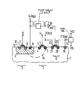
Fi~ure 1 shows an integrated circui~ of the inven~ion
which is constructed on a semiconductor substrate 1 of doped
semiconductor material, for example p-conductive silicon. The
substrate 1 has a~ n-conductive, well-shaped semiconductor zone
2 which extends up to the boundary surface la of the substrate
1. Outside of the semiconductor zone 2, n -doped semiconductor
regions 3 and 4 are inserted into the substrate 1, these
forming the source and drain regions of an n-channel field
effect transistor T1. The channel region lying between regions
3 and 4 is covered by a gate 5 which is provided ~ith a
terminal 6 and which is separa~ed from the boundary surface la
by a thin, electrically insulating layer 7 o~, for example,
SiO2. The source region 3 is connected to a termlnal 8 which
lies at a ground potential Vss. Further, p -doped regions 9
and 10 are inser~ed into the ~emiconductor zone 2, the~e
representing the source reglon and the drain region of a p-
3a
- ~ 275~57
channel field effect transistor T2. The channel region
lying between the regions 9 and 10 is covered by a gate 11
which is provided with a terminal 12 and which is separated
from the boundary surface la by a thin, electrically
insulating layer 13 of, for example, SiO2. The source
region 9 of T2 is connected via regions 2 and 15 to a
terminal 14 which is wired to a supply potential VDD. The
semiconductor zone 2 lies at the supply voltage VDD via the
n -doped contact region 15 which is in communication with
the terminal 14.
A substrate bias generator 16 is also provided, this
generating a ne~ative substrate bias of, for example, -2
through -3 volts. The output 17 of the substrate bias
generator is connected to a p -doped contact region 18 which
is inserted into the semiconductor substrate 1. The
semiconductor substrate 1 is thus held at the negative
substrate bias generated by 16, whereas the source regions,
for example 3, of the transistors, for example T1, situated
in the semiconductor substrate 1 are connected to ground
potential Vss. What is achieved, among other things, is
that the depletion layer capacitances of the source regions
of the transistors arranged in the substrate 1 are
diminished.
In order to avoid a latch-up effect which could occur
within the four-layer structure 3, 1, 2 and 9 lying along
the broken line 19 between the terminals 8 and 14, the
output 17 of the substrate bias generator 16 is connected to
a circuit point situated at ground potenti.al, being
connected thereto via an electronic switch S1. In the
illustrated exemplary embodiment, this circuit point is the
terminal 8. In detail, the output 17 in the arrangement of
Fig. 1 is connected to an n+-doped semiconductor region 20
--4--
~ ~7S4~7
which is inserted into the semiconductor substrate 1. A
further n -doped semiconductor region 21 inserted into the
semiconductor substrate 1 is connected to the circuit point,
i.e., to the terminal 8, lying at ground potential. The
region of the semiconductor substrate 1 lying between the
regions 20 and 21 is covered by a gate 22 which is separated
from the boundary surface la by a thin, electrically
insulating layer 23 of, for example, SiO2. Together with
the parts 22 and 23, the regions 20 and 21 form an n-channel
field effect switching transistor which represents the
electronic switch Sl.
The drive of Sl is provided via a time-delay circuit 24
whose input lies at the terminal 14 and whose output 25 is
connected to the gate 22 via an inverting amplifier 26. At
the time that the supply voltage VDD is applied via the
terminal 14 when the circuit is placed in operation, then
the inverter 26 connected to 14 at first produces an output
level roughly corresponding to VDD and places the switch Sl
into its conductive condition, as long as the output 25 of
the time delay unit 24 remains at the ground potential Vss,
which it exhibits in its quiescent condition. Via Sl, the
output 17 of the substrate bias generator 16 and, thus, the
substrate 1 are held at the ground potential Vss of the
circuit. Only when the time-delay circuit 24 reacts to the
supply voltage VDD applied to the input side, after a
prescribed delay time, such that it emits a higher voltage
level via its output 25 such that the output of the inverter
26 is switched to a low output voltage, is the switch Sl cut
off.
The drive of Sl set forth above thus determines that the
substrate 1, after the application of the supply voltage,
lies at a potential corresponding to the ground potential
--5--
~ 2'~57
Vss during a delay time prescribed by the time-delay circuit
24. Only after the expiration of the delay time can the
substrate 1 be charged with the bias supplied by the
substrate bias generator 16 and supplied via 17 and 18,
being charged therewith because the switch S1 is then
inhibited. When the duration of the said delay time is
dimensioned such that S1 is not cut off until the full,
negative bias has built up at the output 17 of 16, the risk
of the occurence of a latch-up effect when the supply
voltage is connected is eliminated.
Fig. 2 shows a preferred embodiment of the time-delay
circuit 24 and of the inverter 26 of Fig. 1 which can be
integrated on the semiconductor substrate 1 in a simple
way. An n-channel field effect transistor T3 and a load
element 27 are provided, the latter being formed by a p-
channel field effect transistor whose gate is connected to
its drain terminal. The source terminal of this transistor
is conducted to the terminal 14 connected to VDD, whereas
its drain terminal is connected to the gate of T3. The
source and drain terminals of T3 are connected to one
another and are connected to the terminal 8 lying at ground
potential Vss. Together with the load element 27, the
transistor T3, acting as a capacitance, forms a RC element
which represents an especially simple realization of the
time-delay circuit 24. The output 25 of circuit 24 is then
applied via the amplifier 26 to the gate of the n-channel
field effect transistor forming the switch S1. The
amplifier 26, fashioned as an inverter, contains a series
circuit of a p-channel field effect transistor T4 and an n-
channel field effect transistor T~, whose gates are
connected to the output 25 of the time delay unit 24. The
upper terminal of T4 is connected to terminal 14 via a load
--6--
~ Z75~7
element 28 and the lower terminal T5 is connected to -the
terminal 17. The load e~ement 28 is expediently realized as
a p-channel field effect transistor whose gate is wired to
its drain terminal. The electronic switch S1, in accord
with Fig. 1, is inserted between the circuit points 17 and
8, and its gate is connected to the junction of T4 and T5.
When, after VDD has been connected to the terminal 14, the
voltage at 25 has risen to a value which corresponds to the
threshold voltage of T5, the gate of Sl is supplied with the
voltage VBB via the transistor T5 which is then conductive,
so that S1 inhibits, i.e., is cut off.
In a departure from the embodiment set forth above, the
electronic switch Sl can also be realized in some other way,
for example as a bipolar transistor which may be executed as
an external circuit element and wired to the terminals 8 and
17 via connecting lines.
In addition to the embodiments set forth above, the
invention also contemplates embodiments wherein n-conductive
substrates are provided with p-conductive, well-shaped
semiconductor zones. The conductivity types of all
semiconductor parts and the polarities of all voltages are
thereby replaced by their respectively opposite conductivity
types and voltages.
A preferred application of the invention is found in
periphery or interface circuits for dynamic semiconductor
memories having high packing density which are
monolithically integrated with the memory cells.
It will be apparent that various modifications and/or
additions may be made in the apparatus of the invention
without departing from the essential feature of novelty
involved, which are intended to be defined and secured by
the appended claims.
--7--