Note: Descriptions are shown in the official language in which they were submitted.
~ Z75~
TITLE OF THE INVENTION
APPARATUS AND METHOD FOR MOUNTING CIRCUIT ELEMENT ON
PRINTED CIRCUIrr BOARD
BACKGROUND OF THE INVENTION
Field Or the Invention
Thls invention rela-tes -to an apparatus and method for
mounting a circuit element on a substrate, and more
particularly to an apparatus and method for a surface
mounting-type electronic circuit element such as a Flat
Plastic Package component (hereinafter re~erred to as "FPP"),
a Plastic Leaded Chip Carrier component (hereina~ter referred
to as "PLCC"), a Leadless Chip Carrier component (hereinafter
referred to as "LCC"), a Small Outline Integrated Circuit
component (hereinafter referred to as "SOIC") or the like
on a substrate or a printed circuit board with high accuracy.
Description of the Prior Art
Such a conventional circuit element mounting apparatus
is adapted to carry out positioning of a printed circuit
board with respect to the apparatus by means of a positioning
hole formed on a surface of the board. Also, positioning
of a mounting head is carried out on the basis of origins
of X and Y coordinates of an X-Y table head on which the
mounting head is mounted. In the conventional mounting
apparatus, a positional relationship between the positioning
hole of the printed circuit board and a conducting pattern
(wiring pattern) on the printed circuit board is deemed
~ .
- ' ~
'
"'. ' ' '~
'
., : ` . ' ~ '
--2--
to be not varied depending on a printed circuit board and
likewise a relative positional relationship between the
posi-tioning hole and -the origins of the X and Y coordinates
Or the X-Y table head is deemed to be constant irrespective
of` a printed circuit board.
The positioning hole of the printed circuit board is
formed by drilling subsequently to formation of -the
conducting pat-tern, resulting in a positlonal error in the
formation Or the hole being as large as about 0.3mm. This
causes misregistration as 1arge as 0.3mm to occur between
the amoun-t of movement of the rnounting head to a circuit
elemen-t mounting posi-tion on the prlnted circuit board and
the actual circuit element mounting position. Unfortunately,
the relative positional relationship between the positioning
hole and the origins of the X-Y table which is merely kept
constant in the conventional apparatus fails to prevent
the misregistration. The misregistration of about 0.3mm
often causes a failure in connecting of a surface
mounting-type circuit element called an FPP, a PLCC, an
LCC or an SOIC with respect to a substrate, because it is
so constructed that an interval between lead wires of the
circuit element is small.
Also, the deviation of the positioning hole on the
printed circuit board causes mounting of a circuit element
on the printed circuit board to be carried out at a wrong
posture.
, ~ " .' ' -
- ' ~ ~:, ' .
'- . ~
:~.2'~55~1
--3--
SUMM~RY OF THE INVENTION
The present invention has been made in view of the
foregoing disaclvantages of the prior art.
Accordlngly, it is an object of the present invetion
to provide an apparatus and method for mounting a circuit
element on a substrate which is capable of mounting a circuit
element on a substrate with high accuracy.
It is another object of the present invention to provide
such an appara-tus which is capable Or racilitating supply
Or a circuit element, particularly, a surrace-mounting type
circuit element such as an FPP, a PLCC, an LCC, an SOIC
or the like to a predetermined circuit element extracting
position.
It is a further object of the present invention to
provide such an apparatus which is capable of discretely
supplying circuit elements one by one with a simple
structure.
It is still another object of the present invention
to provide such an apparatus which is capable of allowing
even a chlp-like circuit element to be intermittently carried
to a predetermined circuit element extracting position
without any trouble while being kept at a correct posture.
It is yet another object of the present invention to
provide such an apparatus which is capable of carrying out
disposal of an empty storage tape from which circuit elements
~. ~ 7 ~
have been removed while ensuring smooth operation of other
mechanisms such as a tape supply mechanism and the like.
It is still a further object of the present invention
to provide such a method which is capable of ~acilitating
centering of` a circuit element, particularly, a
surface-mounting type circuit element without deforming
or bending its lead wires.
In accordance with one aspect of the presen-t invention,
an apparatus for mounting a circuit element on a substrate
includes a circuit element supply mechan:ism for supplying
a circuit element to a predetermined position of the
apparatus, a centering and optional turnlng mechanism for
regulating a position and a posture of the circuit element
and a circuit elemen-t extracting head arranged so as to
be movable between the predet.ermined position and arranging
position of the centering and optional turning mechanism.
The extracting head is adapted to extract the circuit element
from the supply mechanism by suction and deliver it to the
centering and optional turning mechanism. Also, the
apparatus includes a mounting head arranged so as to be
movable with respect to a printed circuit board. The
mounting head is adapted to hold thereon the circuit element
of the position and pos-ture have been regulated by the
centering and optional turning mechanism by suction and
carry it to the printed circuit board. Further, the
apparatus includes a substrate support mechanism for
~.~
,: ' ' ~' . ' , . ,
'
:
~ 2'7556~
supporting thereon the prin-ted circuit board on which the
circuit element is to he mounted, a lead wire detection
mechanism for detecting lead wires of the circuit elemen-t
of which the position and posture have been regulated by
the centering and optional turning mechanism, and a substrate
mark detection mechanism for detecting a mounting reference
mark on the printed circuit board suppor-ted on the substrate
support mechanism. Thus, the apparatus allows movement
of the mounting head with respect to the printed circuit
board to be corrected depending on a result Or detection
by each of the detection mechanisms.
According -to a further aspect Or the presen-t invention,
there is provided a method for mounting a circuit element
on a printed circuit board, comprising the steps of supplying
a circuit element to a predetermined position of an automatic
mounting apparatus; transferring the circuit element from
the predetermined position to a centering and optional
turning mechanism incorporated in the mounting apparatus
to carry out the centering and turning of the circuit element
by four claws, the four claws being mounted on the centering
and optional turning mechanism and being arranged so as
to be opposite to four sides of a circuit element; delivering
the circuit element to a mounting head; conveying a printed
circuit board to a stop position; and mounting the circuit
element on the printed circuit board when is at the stop
position; the step of centering and optional turning Or
~;~'7~56
--6--
the circuit element by the four claws comprising holding
two sides of -the circuit element parallel -to each other
between one pair of claws of the four claws positioned
oppositely to the two parallel sides of the circuit elemen-t
through a tip end of each of lead wires projecting from
the two parallel sides or a body of the circuit element
and then separating the two claws from the lead wires or
the body, and thereafter holding the remaining two sides
of the circuit element between the other pair of claws
through a tip end o~ each of lead wires projecting from
the remaining two sides or the body.
BRIEF DESCRIPl`[ON OF T~IE DRAWINGS
These and other objects and many of the attendant
advantages of the present invention will be readily
appreciated as the same becomes better understood by
reference to the following detailed description when
considered in connéction with the accompanying drawings
in which like reference numerals designate like or
corresponding parts throughout; wherein:
Fig. 1 is a perspective view generally showing an
embodiment of an automatic circuit element mounting apparatus
according to the present invention;
Fig. 2 is a plan view showing positioning hoLes and
mounting reference marks provided on a printed circuit board;
Fig. 3 is a schematic plan view showing four claws
of a centering and optional turning mechanism incorporated
:
.
.
. .
3.~7S56
--7--
in the moun-ting apparatus Or Fig. 1;
Fig. 4 is a schematic plan view showing lead wires
of a circuit element displayed by a lead wire detecting
camera;
Fig. 5 is a flow chart showing operation of -the
automatic circuit element mounting apparatus shown in Fig.
1 ;
Fig. 6 is a schematic plan view showing a posture of
a circuit element;
Figs. 7 to 9 each are a schematic view showing
preliminary -turning of a circuit element by a centering
and optional turing mechanism;
Fig. 10 is a sectional front elevation view showing
a centering and optional turning mechanism;
Fig. 11 is a front elevation view showing the centering
and optional turning mechanism Or Fig. 10;
Fig. 12 is a plan view showing a claw holding plate
and positioning claws of the centering and optional turning
mechanism;
Fig. 13 is a plan view showing a modification of the
positioning claws of Fig. 12;
Fig. 14 to 16 each are a plan view showing operation
Or the centering and optional turning mechanism of Fig.
10;
Fig. 17 is a schematic view showing a manner Or
inspection or detection of lead wires;
-, . . :~ . :
,
: -: ` :
2'7~ 5
--8--
Fig. 18 is a schematic view showing image processing
in the lead wire detection;
Fig. 19 is a schematic view showing image processing
in inspection or detection of` misregistration a circuit
element and a mounting head in holding of the circuit element
on the mounting head by suction;
Fig. 20 is a schematic view showing an optical
processing system to which correction of misregistration
is applied;
Fig. 21. is a schematic view sllow:ing irradiation :in
the optical processing system of' Fig. 20;
Fig. 22 is a schematic view showing an irradiation
mechanism which is adapted to carry ou-t irradiation of Fig.
22;
Fig. 23 is a schema-tic view showing a reference pattern
of a TV projector used in image processing;
Fig. 24 to 29 each are a schematic view showing image
processing by the TV projector of Fig. 23;
Fig. 30 is a schematic view showing misregistration
data operation depending on coordinates by the TV projector
of Fig. 23;
Fig. 31 is a front elevation view showing a tray
carrying mechanism or unit for supplying circuit elements;
Fig. 32 is a front elevation view partly in section
showing an essential part Or the tray carrying unit shown
in Fig. 31;
~i~7~;5~i9
g
Fig. 33 to 35 each are a front elevation view showing
operation Or the tray carrylng unit shown in Fig. 31;
Fig. 36 :is a side elevation view showing a stick feeder
used for supply of a circuit element;
Fig. 37 is a sectional side elevation view showing
an essential part of the stick feeder shown in Fig. 36;
Fig. 38 is a plan view showing a train of circuit
elements supplied by a tate feeder;
Fig. 39 is a sectional front elevation view showing
the circuit element tra:in Or Fig. 38;
Fig. 40 is a front eleva-tion view showing a tape feeder;
Fig. 41 iS a sectional plan view showing an essential
part of the tape feeder of Fig. 40;
Fig. 42 is a sectional side elevation view showing
a take-up reel;
Fig. 43 is a sectional side elevation view showing
a pitch feed wheel;
Fig. 44 is a front elevation view showing operation
of a r-atchet mechanism attached to the pitch feed wheel
of Fig. 43;
Fig. 45 is a plan view showing an air cylinder assembly
for actuating the ratchet mechanism of Fig. 4LI;
Fig. ll6 is a sectional view taken along line II-II
of Fig. lll which shows a mechanism for supporting the train
of circui-t elements shown in Figs. 38 and 39 at a circuit
element extracting position;
`
:: ,
, .
~ Z 7 ~tj~ ~
--10--
Fig. 47 is a sectional view showing a modification
of the supporting mechanism shown in Fig. 46;
Fig. 48 is a sectional front elevation view showing
an upper tape guide assembly;
Fig. 49 is a front elevation view partly in section
showing a tape cutting mechanism or unit; and
Fig. 50 is a sectional front elevation view showing
an essential part of the tape cutting unit of Fig. 49.
DETAILED DESCRIPTION OF THE PREFERRED ÆMBODIMENT
An automatic circuit element mounting apparatus according
to the present invention will be described hereinafter
with reference to the accompanying drawings.
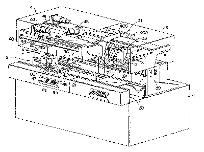
Fig. 1 shows a general structure of an embodiment
of an automatic circuit element mounting apparatus according
to the present invention. An apparatus of the illustrated
embodiment includes a base 1, a substrate carrying mechanism
or unit 2 arranged on a front side of the base 1 so as
to carry printed circuit boards in turn, a circuit element
supply mechanism or unit 4 on a left side of the base 1.
Also, the apparatus includes televisions 50 incorporated
in a picture processing mechanism or unit and positioned
above the front portion of the base 1. In Fig. 1, only
telescreens are shown for the televisions 50.
~'.~
~.~ J
.
,
~ . "' ' ' ' ', ' ' ~,, .
.: '
: . ! ' -
- ., . . ~ .
'- ' '- ' '' ,
i 2~
The substrate carrying mechanlsm 2 includes a palr
of support frames 20 mounted on the base 1 and a belt
conveyor 21 provided on each of inner surfaces Or the support
frames 20 opposite to each other. The substrate carrying
mechanism 2 is adapted to insert a positioning pin (not
shown) into a positioning hole H of a printed circuit board
P (Fig. 2) at a substrate stopping position or substrate
locating position to securely hold the board P.
The circui-t elemen-t supply mechanism 3 comprises both
a tray feeder 30 f`or supplying surface-mounting type circuit
elements E such as an FPP, a PL,CC, an LCC, an SOIC and the
like and a stick feeder 31 or a tape ~eeder (in Fig. 1,
a stick feeder 31 is shown).
The tray feeder 3~ is adapted to arrange a plurality
of trays 32 in a stacked manner each having circuit elements
E arranged in rows thereon. The -tray feeder 30 is forward
moved one pitch every time when foremost circuit elements
on an uppermost tray are taken out or extracted therefrom
at a circuit element extracting position V, so that a
subsequent row of circuit elements on the tray rnay be
transferred to the extracting position.
The stick feeder 31 is constructed to store circuit
elements in a staeked manner in a reetangular eylinder-li}ce
stiek ànd carry lowermost one of the circuit elements to
the eireuit element extracting position V by means of a
belt feeder.
'".- ' ~' " ~ , '
.
~1 2'755~
The tape feeder includes a tape having circuit elements
held thereon in a row in the longitudinal direction of the
tape and being wound on a reel, and is adapted to feed the
circuit elements carried on the tape to the circuit element
extracting position V in turn.
The apparatus of` the illustrated embodiment also
includes a circui-t element ex-tracting mechanism 6 mounted
on an X-Y table 33 movably arranged on the base 1. The
extracting mechanism 6 includes an extracting head 60 which
is adapted to ex-tract a circuit element from the tray feeder
30 by suction, sticlc feeder 31 or tape feeder at the circuit
element extracting position V by means of a suction pin
61 and deliver it to a centering and optional turning
mechanism 7.
The circuit element mounting mechanism 4 is mounted
or assembled on a support frame 40 arranged above the
substrate carrying mechanism 2 in a manner to hang over
it. The support frame 4V is also attached thereto an X-Y
table head 41. More particulary, the X-Y table head 41
includes an X direction slider 44 supported on an X direction
sliding shaft 42 fixed on the frame 40 so as to be slidable
in an X direction and engaged with an X direction ball thread
shaft so as to be actuated by an X axis motor 43 and a Y
direction slider supported on a Y direction sliding shaft
arranged on the X direction slider side so as to be slidable
in a Y direction and engaged with a Y direction ball thread
','~'' ~ - '
" ~ , ' ' ' "'
-
,
- , ,
~:'75
-13-
shaft so as to be actuated by a Y axis motor 45.
The circuit element mounting mechanism 4 also includesa mounting head l~6 fixedly mounted on a lower end of the
Y direction slider. In the illustrated embodiment, the
mounting head ~16 has three suction pins 47 arranged at equal
intervals in the ~ direction. Each of the suction pins
47 is adapted to be vertically moved following curved
configuration of a cam.
On the mounting head 46 is securely mounted a camera
80 of a sustrate mark detection mechanism for de-t~cting
or inspecting a mounting ref`erence mark M formed on the
printed circuit board P simultaneously with forma-tion of
a conducting pattern thereon as shown in Fig. 2. In the
illustrated embodiment, two such mounting reference marks
M are provided to permit a deviation or variation in
parallelism of the printed circuit board P with respect
to the substate carrying mechanism 2 to be effectively
detected. Also, the mounting reference marks M may be formed
together with the conducting pattern by etching, to thereby
keep positional relationships between the conducting pattern
and the mounting reference marks in each of the printed
circuit boards constant.
The centering and optional turning mechanism 7 briefly
described above is arranged along -the substrate carrying
mechanism 2 on the base l. The centering and optional
turning mechanism 7, as shown in Fig. 3, includes
:. , ': ' '
- .' '- '
:,
-14-
four-in-a-set position regulating claws 70 so as to correspond
to a circuit element E held on the suction pin 61 of the
circuit element extracting head 60 and each of the suction
pins 47 of the mounting head 46 and is adapted to actuate
the four claws 70 so as to narrow intervals between the
claws, to thereby regulate lead wires Rl, R2,--- of the
circuit element E, resulting in a center of the circuit
element being aligned with that of the suction pin 47.
At this time, a rotation angle ~ ~Fig. 6) indicating a
posture of the circuit element is set at 0 degree. Then,
when it is required to turn the circuit element E by and
angle of 90 , 180 and 270 or any other desired degrees,
each of the claws 70 is turned correspondingly. The centering
and optional turning mechanism 7 may be constructed to
carry out turning of the circuit element by only angles
of 0, 90, 180 and 270. Alternatively, it may carry
out turning on the element by any optional angle.
The centering and optional turning mechanism 7 has
a camera 90 for a lead wire detection mechanism fixe~ly
mounted on a side theron which serves to detect the lead
weres Rl, R2 --- of the circuit element E after centering.
The camera 90, as shown in Fig. 4, is adapted to project
diagonal corners J and K of the circuit element E, in an
enlarged manner, while switching them, so that position
and rotation of each of the lead wires Rl, R2 --- of the
circuit element E may be detected with high accuracy.
-.
" " ' ', '` ' ' ' .
. , ~ .
-15-
In order to operate the automatic circuit element
mounting apparatus of the illustrated embodiment, data
on a position on the printed circuit board P on which the
circuit element E is to be mounted and a posture at which
the circuit element is to be mounted on the board P are
inputted, to a program controller. For example, the data
on the mounting position may be indicated by X and Y coordinates
of the X-Y table head and that on the mounting posture
may be indicated by the rotation angle 0. The program
controller generates values o~ X and Y coordinates of a
mounting position of the circuit element and a rotation
angle of the circuit element, and the like in a mounting
order and supplies them to the circuit element mounting
mechanism 4 in turn.
The circuit element mounting mechanism 4, substrate
carrying mechanism 2, centering and optional turning
mechanism 7, and circuit element extracting mechanism 6
carry out their operations according to a flow chart shown
in Fig. 5.
More particularly, the circuit element extracting
head 60 of the circuit element extracting mechanism 6 takes
out a circuit element E at the circuit element extracting
position in the circuit element supply mechanism 3, then
delivers it to the centering and optional turning mechanism
7 and finally returns to its original position for the
next extraction.
r
- .: .
-.
. . .
~ ~7SS~
-16-
The centering and optional turning mechanism 7 to
which the circuit element E has been carried then carries
out centering or positional regulation of the circuit element
E by means of the four claws 70 shown in Eig. 3. Prior
to the delivery of the circuit element E to the mechanism
7, preliminary turning of the mechanism 7 may be carried
out to cause wider claws 7Oa and 7Ob to be engaged with
wider sides of the circuit element E, as required. More
particularly, supposing that the clrcuit element E in the
circuit element supply mechanism 3 is at a posture shown
in Fig. 7 and the position of origin of the centering and
optional turning mechanism 7 causes the claws 70 to be
arranged as shown in Fig. 8, the centering and optional
turning mechanism 7 is prepared to receive the circuit
element E from the circuit element extracting head 60 while
the claws 70 are kept at a posture as shown in Fig. 9.
Also, it carries out turning by a predetermined angle of
O, as re~uired.
Then, the mounting head 46 of the circuit element
mounting mechanism 4 takes Ollt the circuit element E indicated
by the program controller from the centering and optional
turning mechanism 7 by means of the suction pin 47 and
holds it thereon by means of suction.
The lead wires of the circuit element E which has been
subjected to the centering and turning treatment are observed
by the camera 9O of the lead wire detection mechanism and
~` .
~j ,
.' . ~ ' :
' ~ ' ,
~'7~ 5
-17-
a picture obtained is supplied to a posi-tion correcting
operation unit or pic-ture processing uni-t.
A printed circui-t board P carried by the subs-trate
carrying mechanism 2 is stopped a-t a predetermined position.
Mounting reference marks M of the so-positioned printed
circuit board P are observed through the camera 80 of the
substrate mark detection mechanism and a picture obtained
is supplied -to the position correcting operation unit.
The pictures obtained by the cameras 80 and 90 are displayed
on telescreens of the picture processing televisions 50.
The position correcting operation unit or picture
processing unit or mechanism which receives a resul-t of
detection by each of the lead wire detection camera 90 and
substrate mark detection camera 80 previously stores therein
data on pictures of the cameras 80 and 90 showing a state
that the circuit element is precisely positioned on a circuit
element mounting position of the printed circuit board,
so that it may carry out comparison between the stored
picture data and an actual picture obtained by each of -the
cameras 80 and 90 to effect a mounting position correcting
operation. This results in positional control of the
mounting head 46 being carried out to obtain corrected X
and Y coordinates and rotation angle ~.
Subsequently, the suction pin 47 is lowered -to mount
the circuit element E on the predetermined circuit element
mounting position of the printed circuit board P.
-.' - '
.2'7~ 5
-18-
Thereafter, the suction pin is raised and -the mounting
head 46 returns -to its original position for the next
mounting operation.
As can be seen from the foregoing, the automatic circuit
element mounting apparatus of the illustrated is so
constructed that one of the cameras detects the mounting
reference marks formed on the printed circuit board
simultaneously with formation of the conducting pattern
thereon and the other camera detects the lead wires of the
circuit element subJected to the centering and optional
turning trea-tment, thus, the amount of movement of the
mounting head is corrected based on the results of detection
of the cameras. Such construction permits mounting of the
circuit element on the printed circuit board to be
accomplished with high accuracy. Also, this substantially
eliminates an error of the circuit element moun-ting position
caused due to misregistration between the conducting pattern
of the printed circuit board and the positioning hole thereof
and a variation in centering and optional turning of the
circuit element. Such advantages are remarkably exhibited
in mounting of a surface-mounting type circuit element in
which an interval between lead wires is narrowed such as
an FPP, a PLCC, an LCC, an SOIC or the like on the printed
circuit board.
The centering of the circuit element is concurrently
carried out with respect to four side surfaces of the circuit
~1.2'75~
-19-
element. However, it may be carried out wlth respect -to
every two side surfaces of -the circuit element in turn.
Such centering effectively prevents deformation or bending
of the lead wires of the circuit element because any lateral
force is not applied thereto.
The construction of the centering and optional turning
mechanism 7 will be described in detail with reference to
Figs. 10 to 16.
The centering and optional turning mechanism 7 includes
a support frame 71 and a hollow shaft 72 rotatably supported
on the support frame 71. In an upper opening of the hollow
shaft 72 is inserted or fitted a circui-t element support
pin 73, which is upwardly biased by means of a compression
spring 74 arranged in the hollow shaft 72, so that a
cushioning effect may be produced on the circuit element
support pin 73. The circuit element support pin 73 is
adapted to place thereon a surface-mounting type circuit
element having lead wires R1, R2, --- extending from four
side portions thereof and securely hold it thereon by
suction.
At an upper end of the hollow shaft 72 is horizontally
fixed a claw holding plate 76 through a mounting member
75, and the circuit element suppor-t pin 73 is projected
through a central hole 76a of the claw holding plate 76.
The claw holding plate 76, as shown in Fig. 12, is formed
with four slit-like cutouts 76b at angular intervals of
.
`
- ` ` '
7S~6~
-20-
90 , at which follr positioning claws 70a to 70d are arranged
so as -to be slidable on a horizontal plane, respectively.
Around an upper portion of the hollow shaft 72 are
in-tegrally formed four brackets 77 at equal intervals, to
which levers 78 are pivotally connected through pins 79,
respectively. The levers '78 each are engaged at a tip end
thereof with each recess 70e of the positioning claws 70a
to 70d. Only one pair of the levers 78 are shown in Fig.
10, however, the other pair of the levers are provided in
a direction perpendicular to the drawing sheet. The levers
'78 each are engaged at a lower end thereof wi-th an annular
spring 700, which acts to constantly force the levers 78
in a direction in which the tip ends or upper ends of the
levers are kept apart from one another.
Also, the hollow shaft 72 has a first annular ac-tuating
member 701 fitted thereon so as to be vertically slidable
thereon to actuate one pair of the levers 78 shown in Fig.
10. For the purpose, the annular actuating member 701 is
engaged at an upper surface thereof with a projection 78a
of each of the levers 78. More particularly, Fig. 10 shows
a state that the annular actuating member 701 is at a
lowermost position, wherein the distal ends of one pair
of the levers 78 are kept apart from èach other by the
annular spring 700, resulting in the positioning claws 70a
and 70b being kept apart from each other. When the annular
actuating member 701 is moved to a raised posi-tion, the
~ ~755;~
-21-
projection 78a of` each of the levers 78 is pushed up,
resulting in the positioning claws 70a and 70b being close
to each other.
The hollow sha~t 72 also has a second annular actuating
member 702 movably f`itted thereon so as to be vertically
slidable thereon and positioned below the first annular
actuating member 701, which serves to actuate the other
pair of the levers provided in a direction perpendicular
to the paper of` Fig. 10. The actuating member 702 i5
upwardly ~orced by means of` a compresslon spring 703. In
Fig. 10, the actuating member 702 likewise is at a lowered
position, resulting in the positioning claws 70c and 70d
being kept apart from each other. When the actuating member
702 is moved to a raised position, the other pair Or the
levers are pushed up, to thereby cause the positioning claws
70c and 70d to be close to each other.
As shown in Fig. 11, on the support frame 71 are
pivotally supported bell cranks 705 and 706 through pins
707 and 708, which are adapted to act as a cam foIlower.
The bell crank 705 is engaged at a distal end thereof with
a groove 701a of the first annular ac-tuating member 701
(Fig. lO) for actuating the positioning claws 70a and 70b,
whereas the bell crank 706 is engaged at a distal end thereof
with a flange-like engagement 702a Or the second annular
actuating member 702(Fig. 10) for actuating the posit:ioning
claws 70c and 70d. Also, the bell cranks 705 and 706 are
' ' :-,
. ' ': ' , ;': '
.'
- . ,
~1 2~5~6~
-22-
abutted a-t lower ends thereof against cam grooves of a cam
plate 710 rotated through a rotating shaf-t 709, respec-tively.
Thus, the bell cranks 705 and 706 are pivotally moved with
rotation of -the cam plate 710 to vertically move ~he first
and second annular actuating members 701 and 702. Vertical
movement of the actuating member 701 is not carried out
at the same timing as that of the actuating member 702,
which will be described hereinafter. On the suppor-t frame
71 is fixed a sensor 711 for detecting a rota-tional position
of the cam plate 710.
As shown ln Fig. 10, the hollow shaft 72 has a bevel
gear 712 fixed on a lower end thereof, which is engaged
with a bevel gear 713 fixed on a rotating shaft of a motor
714 which is then securely mounted on the support frame
71. ~otation of the motor 714 causes the hollow shaft 72,
and the claw holding plate 76 and positioning claws 70a
to 70d mounted on the shaft 72 to be rotated by an optional
angle.
Connected through a joint 715 to the hollow shaft 72
is a hose 716, of which a distal end is connected through
a valve or the like to a vacuum pump (not shown). This
causes suction force to be applied from the pump through
the hose 716 and an interior of -the hollow shaft 72 to the
circuit elemen-t support pin 73.
In the circuit element centering and optional turning
mechanism 7 constructed as described above, when the suction
.
' ?
3~.27S5~
pin l~7 of the circuit elemen-t mounting mechanism 4 carries
a clrcuit element E to a space defined by -the positioning
claws 70a to 70d kept apart from one another, the clrcuit
element support pin 73 upwardly projecting through -the claw
holding plate 76 holds the circui-t element E thereon by
suction. Then, as shown in Fig. 14, the positioning claws
70a and 70b are rendered close to each o-ther to regulate
distal ends of lead wires R1 and R2 extending ~ro~l longer
sides of the circuit elemen-t E. In other words, the distal
ends of the lead wires are interposed between the positioning
claws 70a and 70b.
Then, the positioning claws 70a and 70b are actuated
to be ~ept apart from each other as shown in Fig. 15, and
then the other pair of the positioning claws 70c and 70d
are actuated to be close each other, to thereby regulate
or position distal ends of lead wires of the circuit element
E extending from shorter sides of the circuit element.
More particularly, the distal ends of the lead wires are
securely interposed between the positioning claws 70c and
70d.
Subsequently, as shown in Fig. 16, the positioning
claws 70a and 70b are rendered close to each other again
while the positioning claws 70c and 70d are kept close to
each other, so that the positioning claws 70a to 70d may
interposedly hold.the circuit element E therebetween. Then,
vacuum suction applied to the circuit element support pin
.. . . .
~1 27S5~
-2Ll -
73 f'rom the vacuum pump (not shown) is s-topped -to cause
a center portion of the circuit element E positioned by
the positioning claws -to be sucked by the suction pin 47,
Configuration Or the posi-tioning claws 70a to 70d may
be varied depending upon a shape or dimensions of a circuit
elemen-t. For example, when a circuit element is small-sized,
the positioning claws 70a and 70b, as shown in Fig. 13 may
be formed -to have a width smaller than the positioning claws
70c and 70d~ Also, in the illus-trated embodiment, the
circuit element is positioned through the lead wires.
~lowever, the posi-tioning may be carried out through a body
Or the circuit element.
Thus, the circuit element posi-tioning mechanism 7 is
so constructed that the ~our positioning claws arranged
opposite to the four side portions of the circuit element
having lead wires carry out positioning of the circuit
element in the manner that one pair of the positioning claws
interposedly hold two parallel side portions of the circuit
element therebetween and then are separated from each other,
and thereafter the other pair of the positioning claws
securely lnterpose the remaining two parallel side portions
of the circuit element therebetween. Such construction
of the mechanism effectively prevents lateral force from
being applied to the lead wires of the circuit element,
to thereby prevent deformation or bending of the lead wires.
This results in a failure in the mounting of the circuit
., .' ' ~'' '' -,,
.
~.27~;6~
element on the prin-ted circuit board being eliminated.
Also, such construction, when the circuit element is
a sur~ace-mounting type one having a plurality of lead wires
provided on each of four side portions thereof, allows a
state of projection of the lead wires to be also detected
or inspected during the lead wire detection or inspection
described above.
The lead wire detection or inspection may be carried
out using an inspection mechanism constructed as shown in
Figs. 17 to :L9. Prior to the inspec-tion, a position o~
a circuit element E held on the suction pin 47 is regulated
by -the centering and optional turning mechanism shown in
Figs. 10 to 16, so that the circuit element E may be held
on the suction pin 47 at a state of being previously aligned
with an axis of the suction pin 47. To the so-held circuit
element E is irradiated by a light source 91 arranged
immediately below the circuit elemen-t, so that reflecti.on
of light from lead wires R1, R2, --- Rn of the circuit
element E is captured by means of the camera receiver 90.
As the light source 91 is preferably used a ring-like
illumina`ting lamp, because it carries out uniform irradiation
to all the lead wires R1, R2, --- Rn provided around the
circuit element E. For this purpose, a halogen lamp 91b
may be connected through an optical fiber 91a to the light
source 91. When the camera receiver 90 detects reflection
of light from the lead wires R1, R2, --- Rn, the TV 50
.
. .
, ~ , :. ' -
- . .
,
.
:
~I Z'755;~
-26-
converts an electrical signal into a binary signal -through
a picture processing unit or mechanism 92 to dlsplay thereon
a brilliant picture corresponding to each of the lead wires.
The pictures are displayed in a manner to be arranged in
X and Y directions of a telescreen Or the TV as shown in
Fig. 18. In this instance, when the lead wires have any
defect, the TV fails to project or display any picture
thereon or display a pic-ture of which dimensions are
different from normal lead wires, resulting in defectiveness
of the circuit element being detected. Also, this permits
deformation of the lead wires such as bending to be
ef'fectively detected.
In the inspection, the picture processing unit 92 and
a numerical operation control unit 93 are used to find axial
centers L1, L2, ---, Ln within wid-ths of areas of optical
images B1, B2, ---, Bn at every row of each of X and Y
directions on a telescreen of the TV 50. Then, pitch
intervals A1, A2, ---, An between the respective adjacent
two axial centers L1, L2, ---, Ln are found in turn and then
the average value of the pitch intervals A1, A2, ---, An
is calculated. The average value corresponds -to a
predetermined pitch interval between the lead wires of the
circuit element even if one of the lead wires is bent,
accordingly, whether the lead wires are bent or deformed
is judged due to an operation for comparison be-tween the
average and each of the pitch intervals A1, A2, ---, An.
.~7 ~ 5
-27-
When any bending or deformation is detected, whether i-t is
within a prede-termined tolerance is judged. When it i9 out
of the tolerance, a rejection command is supplied -to the
suction pin 47 to prevent the circuit element from being
mounted on a printed circuit board. The inspection procedures
are applied to each lead wire row in the X and Y directions
in -the same manner, so tha-t only an indefective circuit
element may be mounted on a printed circuit board.
When carrying out, through the TV 50, inspect:ion of`
misregistration between the suction pin 47 and a circuit
element held thereon in addition to the above-descr:ibed lead
wire inspection, a center O in the X and Y directions, as
shown in Fig. 19, is preset on the telescreen of the T~ 50
and then comparison of positional relationship between the
center O and an optical image obtained from each of the lead
wires is made to carry out the inspection. More particularly,
intersections C, G and N between the center lines of the
adjacent end lead wires of the adjacent lead wire rows at
three corners of the respective lead wire rows arranged in
the X and Y directions are found utilizing their optical
images. Then, a center O' of the circuit element is found
using the intersections C and G and a positional error between
the centers O' and O is obtained on the basis of X and Y
coordinates, resulting in misregistra-tion between the center
of the suction pin 47 and that of the circui-t element held
thereon being detected or measured. Actuation of the
~ :
- . . . :
'. ~ - . ' .'' ~ ,: - . :
:.
i6~
-28-
centering and optional turning mechanism depending on a result
of the measurement permits precise centering of the circuit
element held on the suc-tion pin 47. Then, axial center lines
of the lead wires of` the two lead wire rows arranged in -the
X or Y direction are connected to each other utilizing oplical
images thereof, so that deviation of rotational direction
of the circuit element rnay be detected due to misregistration
between each of the connected axial center lines and the
central line in the X or Y direction. When any deviation
o~ -the rotation angle ~ is detected according to the
procedures described above, the numer:ical operation control
uni-t 93 actuates a pulse motor 95 through a pulse motor
controller 94 to rotate a gear 96 engaged with the suction
head 47 by an angle corresponding to the angle ~, so -that
a direction of the circuit element held on the suc-tion head
47 may be corrected.
Thus, the lead wire inspection or detection mechanism
is capable of carrying out the inspection for every circuit
element, so that the mounting head may accomplish mounting
of a circuit element on a printed circuit board with extremely
high precision. This results in highly troublesome
recorrection of the circuit element which is re~uired after
fixing of the circuit element by soldering in the prior art
being eliminated.
The above-described mounting reference mark M on the
circuit element P, when the conducting pattern is formed
- . ' ' , ~: ' . . . .
' ' ' : -
~ 2'7~
-29-
of copper on the printed circuit board by printing, may
likewise be formed of the same material as the conducting
pa-ttern by printing. In this instance, in order to preven-t
oxidation of the ref'erence mark, solder is plated on a surface
of -the mar~s as well as the conducting pattern.
However, the solder formed on -the moun-ting reference
mark generally fails -to have a uniform surface. Accordingly,
when light is irradiated to the printed circuit element rrom
a single light source arranged above -the printed circuit
board, irregular reflectlon occurs on the surface of the
solder to fail to display a correct configuration Or the
printed circuit board on the TV display, thus, an image
displayed on the TV display cannot be used as a control data
for correcting misregistration of the printed circuit board.
It has been found that such a problem is solved by a
substrate misregistration correcting process which is adapted
to radially irradiate light to the whole surface Or the
mounting reference mark formed of the same material as the
conducting pattern, display a random optical image of the
mark on the telescreen of the TV display through the camera,
preset an outer frame line and a center of a reference pattern
corresponding ~o the mounting reference mark at a central
position of the telescreen of the TV display, align the random
optical image of the mounting reference mark displayed on
the telescreen with the outer frame line of the reference
pattern by vertical or up-down adjustment Or a binary level,
-
~ 2'~SS6
-30-
compare a center Or the optical image coincided with thereference pattern with the center of the reference pattern
set on the telescreen of the TV display, and de-tect
misregistration in the X and Y directions between the centers
by means of coordinates of the telescreen to adjust a
positional correlation between the mounting head and the
printed circuit board.
Thus, in the substrate misregistration correcting process
as described above, a large amount Or light is radially
irradiated to the mounting reference mark to display the
random optical image on the telescreen of the TV display
and the optical image is coincided with the outer frame line
of the predetermined reference pattern by up-down ad~ustment
of a binary level, resulting in the mounting reference mark
being optically detected. Accordingly, such process allows
a positional correlation between the mounting head and the
printed circuit board to be precisely corrected even when
a solder is applied to the reference mark by plating.
Now, the substrate misregistration correcting process
will be described hereinafter with reference to Figs. 20
to 30.
In the substrate misregistration correction, a positional
correlation between a printed circuit board P placed on the
belt conveyor 21 (Fig. 1) of the substrate carrying mechanism
and the mounting head ~6 for mounting a circuit element on
the printed circuit board P is corrected by movement of the `
: - - ,
. . . .
'
~2'7~6~
-31-
mounting head in the X and Y directions, to thereby cause
a circuit element to be precisely mounted on a predetermined
position o~ the conducting pattern of the printed circuit
board. Also, irradiation of ligh-t is carried ou-t with respec-t
to the mounting reference marl~ M formed of copper which is
the same material as the conducting pattern, so that light
reflected on the mark is used to form the optical image ~hich
is then subJected to image processing to obtain a cla-ta for
posi-t:ional correction of the mounting head l~6.
The image processlng may be carried out using a system
shown in Figs. 20 and 21. More particularly, the system
is adapted to reflect light emitted from an incadescent lamp
82 connected to an elec-tric source 81 on a mirror 83 to
irradiate the light to a substantially central portion of
a mounting reference mark M of a printed circuit board P.
Also, the system is adapted to irradiate light to the mounting
reference mark M from a plurality of LED lamps 85 connected
to an electric source 84. The LED lamps 85, as shown in
Fig. 22, are preferably arranged in a manner to be
substantially concentric with the mounting reference mark
M to radially irradiate a large amount of light to the
reference mark M ~rom the lamps 85 as well as the incadescent
lamp 82. The light reflected on the reference mark M is
guided through a lens 86 to the camera 80 and then supplied
through the image processing unit 92 operated by an operator
to the TV receiver 50. The image processing unit 92 is
.,. , -
.'. ' . :
., ~ . .
7~S~
-32-
connected to the numeral operation control unit 93 and the TV
receiver 50, as sllown in Fig. 23, has a reference pattern preset
in X and Y directions thereon which comprises a center O and
an outer frame line F of widths Wl and W2 corresponding to the
mounting reference mark M formed on the printed circuit board
P by printing.
The image processing system is adapted to display an optical
image I, which is formed by the reflected ligh-t of the reference
mark of the printed circuit board randomly captured by the camera
80, on the telescreen of the TV receiver 50 at a binary level
by means of an electrical signal and judge, by operator's observation
through the numerical operation control unit 93 and TV receiver
50, whether an optical I" prior to adjustment as described hereinafter
coincides with the outer frame line F of the reference
pattern. When the optical image I" overflows the outer frame
line F of the reference pattern as shown in Fig. 24, it is
narrowed, by down adjustment of the binary level, through an
optical image I' (Fig. 25) to an optical image I (Fig. 26)
which substantially coincides with the outer frame line F of
the reference pattern in X' and Y' directions while being
displayed on the telescreen of the TV receiver 50. On the
contrary, when the optical image I" randomly captured by the
camera 80 is displayed in a reduced-size manner wi-thin the outer
frame line as shown in Fig. 27, it is gradually enlarged by
adjustment of the binary level through an optical image
..., ... ~
.
;56~
I' (Fig. 28) to an optical image I (Fig. 29) which
coincides with the outer frame line F of the reference
pattern in the X' and Y' directions while being displayed
on the telescreen of the TV receiver 50. Also, a center
O' of each of the so-obtained optical images I coinciding
with the outer frame line F of the reference pattern is
found through the numerical operation control unit 93
and the TV receiver 50 by an operator, and the nulnber
of differences based on coordina-tes xl, x2 ? ~ n, yl,
y2, ---, yn be-tween each Or so-obtained cen-ters O' and
O' and the predetermined center O of the rererence pattern
is calculated through the picture processing unit 92
serving as an image sensor and the numerical operation
control unit 93 to obtain the amount of' misregistration
therebetween. Based on the so-obtained misregistration
data, the mounting head 46 is positionally adjusted in
relation to the printed circuit board placed on the
conveyor and then lowered to mount the circui-t element
held thereon on the printed circuit board, so that the
circuit element may be precisely positioned with respec-t
to the conducting pattern on the printed circuit board
and fixed thereon by soldering.
Thus, the substrate misregistration correcting process
allows ~ da-ta for positloning the printed circuit board
to be precisely obtained although the ~rinted circuit
f~7C?s, f'~ ~?~,?e ~/
board placed on the conveyor is @i~ e~e~-depending upon
: . .
~,"~ "` '',
"`
~.2t~5~
-34-
the mounting reference mark formed of the same material
as the conducting pattern, so that surface-mounting of
the circuit element of the printed circuit board may be
carried out with extremely high precision.
In the automatic circuit element mounting apparatus,
it is desired that the tray feeder 30 briefly described
above is contructed to readily cope with a variation
in intervals of arrangement of surface-mounting type
circuit elements on the tray 32 which is caused due ~o
a change of the circuit elements, because intervals of
arrangement of the circuit elements on the tray 32 are
varied depending on their shape. Also, in such an
automatic mounting apparatus, a plurality of trays are
arranged in a stacked nammer, so that empty trays from which
circuit elements have been removed are automatically taken out.
For this purpose, the tray feeder 30 constructed
as shown in Figs. 31 to 35 may be employed for the
automatic circuit element mounting apparatus of the
illustrated embodiment.
More particularly, the tray feeder 30 includes a pair of
rails 10 mounted on the base 1 as shown in Figs. 31 and 32.
Also, the unit includes a support 300 which has four brackets 301
fixed on a lower surface thereof. The brackets 301 each have a
roller 302 rotatably mounted thereon through which the unit is
.
55~
moved along the rails l0. In Fig. 31, an arrow Y indicates a
direction of forward movement of the unit.
The tray carrying unit also includes a means for moving the
support 300, which comprises a ball thread shaft 303 provided
below the support 300 and a motor 304 mounted on the support.
More particularly, the ball thread shaft 303 are rotatably
supported at both ends thereof on bearings 305 and 306 fixed on a
lower surface of the support 300 and the motor 304 is securely
mounted on the support 300. The ball thread shaft 303 and a
rotating shaft of the motor 304 have belt pulleys 307 and 303
fixed thereon, respectively, between which a timing belt 309 is
stretched. The ball thread shaft 303 is engaged at a middle
portion thereof with an internally threaded member 11 fixed on
the base 1. Thus, when the motor 304 is driven, rotating force
of the mo-tor is transmitted through the belt pulley 308, timing
belt 309 and belt pulley 307 to the ball thread shaft 303, so
that a positional relationship of the ball thread shaft 303 to
the internally threaded member 11 may be varied to cause the
support 300 to be moved on the rails 10 with respect to the
stationary base 1.
On the support 300 are fixedly mounted two vertically
extending guide snafts 310 which are arranged in a direction
perpendicular to that of movement of the tray carrying unit.
Accordingly, only one shaft 310 is shown in Figs. 31 and 32. On
the guide shafts 310 is vertically slidably supported an elevator
311.
-36-
In the illustrated embodiment, a tray 32 is formed into a
rectangular shape and formed with a plurality of recesses for
placing therein surface-mounting type circuit elemen-ts E at
regular intervals. A plurality of the trays 32 (for example, ten
such trays) each having a plurality of the circuit elements
positioned thereon are placed on the elevator 311 in a stacked
manner. On -the support 300 is pivotally mounted a holding member
312 through a brace 313 at a position in proximity to a distal
end of the elevator 311, which serves to hold an uppermost tray
so as to prevent it from moving.
The tray carrying Ullit also includes a tray takiny-out head
314 fixedly mounted on the base 1 so that it may be opposite to
the tray 32 when the support 300 is moved in a rearward direction
opposite to the forward direction indicated by the arrow Y in
Fig. 31. The tray taking-out head 314 has a suction pin 315
mounted at a lower end thereof in a manner to be vertically
movable, which serves to hold the tray 32 thereon by suction.
Vertical movement of the suction pin 315 may be carried out by
means of, for example, an air cylinder or the like.
Also, on the support 300 is securely mounted a tray
discharge box or frame 316 at a position behind the elevator 311.
The aforementioned circuit element extracting head 60 is
arranged opposite to the trays 32. The extracting head 60 is
adapted to be moved not in the direction indicated by the arrow Y
but in a direction perpendicular to the Y direction or indicated
at X in Fig. 31. The suction pin 61 of the head 60 is vertically
.. . .
2~
-37-
movable.
In addition, the tray carrying unit, as shown in Fig. 32,
includes a positioning plate 12 mounted on the base l to extend
over a range of movement of the support 300. The positioning
plate 12 serves to forward move the support 300 by a distance
corresponding to the interval between -the circuit elements
arranged on the tray. The positioning plate 12 is formed with a
plurality of recesses 13 each having a width corresponding to the
interval S between the circuit elements. The recesses 13 are
optically, magnetically or mechanically detected by a sensor 317
fixedly mounted on the support 300.
~ urther, the tray carrying unit, as shown in Fig. 31,
includes limit switches LS1, LS2 and LS3 arranged on the base 1
along the rails 10 in turn. The limit switches LS1, LS2 and LS3
are adapted to detect a first stop position or foremost stop
position of the support 300, a second stop position or rearmost
stop position thereof, and a third stop position thereof or a
stop position of the support 300 sligh-tly in front of the
rearmost stop position, respectively. For this purpose, the
limit switches are positioned corresponding to these stop
positions, respectively. The foremost stop position
corresponds to a position at which the circuit element
extracting head 60 holds each of circuit elements of a
rearmost row thereon, and the rearmost stop position
corresponds to a position at which the tray talsing-out head
314 holds thereon an empty tray ~rom which circuit elements
are removed by the extracting head 60. The third stop position
3 ~'~5 S6
-38-
corresponds to a position at which the head 60 holds thereon each
of circuit elements of a foremost row by suction. The limit
switch LS1 is actuated when a projection 301a provided on an
inside of the front bracket 301 is abutted against the switch,
and the limit switches LS2 and LS3 each are actuated by a
projec-tion on an inside of the rear bracket 301.
As shown in Fig. 32, on the support 300 is mounted a motor
318 for the purpose of vertically moving the elevator 311. The
motor 318 has an eccentric disc-like cam 319 fixed on a rc>tating
shaft thereof. Against the cam 319 is abutted a rol]er 320 which
serves as a cam follower. The roller 320 is pivotally mounted on
a vertically movable slider 321. The slider 321 is vertically
movably supported on slider bearings 322 fixed on the support 300
so as to upwardly extend therefrom. Also, the slider 321 has a
pinion 323 rotatably mounted thereon, which is adapted to be
engaged with a rack 324 vertically mounted on the support 300 and
a rack 325 fixed on the elevator 311 and arranged in parallel
with the rack 324. The so-constructed pinion and rack mechanism
serves to enlarge vertical movement of the roller 320.
~ ccordingly, when the motor 318 is driven in order to
vertically move the elevator 311 from a position shown in Fig.
32, the cam 319 is rotated and the slider 321 is raised together
with the roller 320, so that the pinion 323 may be rotated in a
right or clockwise direction in Fig. 32 because the right-side
rack 324 is stationary. Such rotation of the pinion 323 causes
the left-side rack 325 to be raised by a distance corresponding
I` : ` :
:
-39-
to a thickness o~ the tray 32.
Now, the manner of operation of the tray carrying unit will
be described hereinafter with reference to Figs. 31 to 35.
An arrow Z above the trays 32 in Fig. 31 indicates a range
at which the circuit element extracting head 60 takes out a
circuit element E from the tray. When starting supply of circuit
elements on the uppermost tray 32, the support 300 is at the
rearward position at which the rear bracket 301 actuates the
limit switch LS3, resulting in the extractin~ head 60 being
positioned above a left end of the range Z or circuit elements of
the foremost row on the tray 32. ~s described above, the head ~0
is not adapted to be moved in the direction indicated at the
arrow Y in Fig. 31. Then, the head 60 is lowered to hold a
circuit element thereon by suction, raised and then moved in the
X direction perpendicular to the Y direction to carry out the
circuit element extracting operation.
When supply of the circuit elements of the foremost row on
the tray is completed, the motor 304 is driven to rotate the ball
thread shaft 303 to cause a positional relationship of the ball
thread shaft 303 to the internally threaded member 11 to be
varied, resulting in forward movement of the support starting.
Then, when the sensor 317 detects the recess 13 of the
positioning plate 12 which coincides with the interval S between
the circuit elements, actuation of the motor 304 is stopped.
This causes the support 300 to be forward moved by a distance
corresponding to the interval S, resulting in circuit elements
,
,
- , . ~
: ' ' ' ' . :
ii5;~i~
-40-
Or a second row on the tr~y being positioned opposi-te to -the
extracting head. Then, the head takes out the circuit elements
of the second row from the tray in turn.
The same operation is repeated to carry out extraction of
circuit elements o~ -third to rearmos-t rows in turn.
Subsequently, the support 300 is moved to the rearmost stop
position at which the rear bracket 301 actuates the limit switch
LS2. This causes the head 60 to be at a position out of the left
end of the tray 32 as shown in Fig. 33 and the holder 312 to
pivotally fall sideways, to thereby be released from engagement
with the tray. Then, the tray taking out head 31~ is lowered,
actuated to hold the uppermost tray thereon by suction and then
raised. Then, the holder 312 is pivotally moved to its original
position to hold the remaining trays 32 on the elevator 311 in
turn.
Thereafter, the support 300 is moved to -the slightly forward
position at which the rear bracket 301 actuates the limit switch
LS3, so that the circuit element extracting head 60 is positioned
opposi-te to circuit elements E of a foremost row on a second
tray as shown in Fig. 34. When the motor 318 starts, the cam 319
is rotated to upwardly move the slider 321 and rotate the pinion
323 to raise the rack 325, so that the elevator 311 may be raised
by a distance corresponding to a thickness of one tray, resulting
in the second tray being lifted to a level at which the removed
uppermost tray was positioned. Then, the extracting head 60
starts taking-out of circuit elements of a foremost row on the
- -
second tray. Circuit elements of second to rearmost rows are
extracted from the tray in turn in the same manner as described
above.
At a s-tate shown in Fig. 35 that all circuit elements on the
second tray 32 have been taken out and the support 300 is at the
foremost position, the uppermost tray is positioned above the
tray discharge box 316. Then, suction of the tray by the tray
taking-out head 314 is released to drop it into the box 316.
Then, the support 300 is returned to a state shown in Fig.
33 and the tray taking-out head 314 holds the second tray thereon
by suction. Subsequently, the extracting head 60 carries out
extraction of circuit elements on a third tray in a manner
described above.
In the tray carrying unit described above, the positioning
plate ~ formed with a marking which comprises the recesses 13
each having a width coinciding with the interval S between the
circuit elements are used as a positioning means. ~owever, the
marking may comprise projections or holes instead of the recesses
13.
As described above, the tray carrying unit is so constructed
that the elevator on which the trays are placed is carried on the
support horizontally movable on the rails, to thereby permit the
circuit elemènt extracting head to accomplish the e~traction at
constant positions. Also, exchange of the positioning means
provided with the marking coinciding with the intervals between
the circuit elements arranged on the tray permits a distance of
~' ' , ' ~' '.
.
~ 27~;7~
ll2
movement of the tray to be varied as desired. Further, the -tray
taking-out head allows empty trays from which circuit elements
have been removed to be automatically taken out at high
efficiency, because the taking-out can be carried out in parallel
with supply of circuit elements.
In the illustrated embodiment, the stick feeder 31
brierly described above may be constructed in such a manner as
shown in Figs. 36 and 37.
More particularly, the stick feeder 31 includes a magazine
support frame 401 which is mounted on the base 1 and adapted to
support thereon a plurality of circuit element magazines 400 in a
stacked manner. llhe magazines 400 each are formed o~ plastic,
metal or the like into a cylindrical shape and adapted to
receive therein circuit elements E in a row. The magazine
support frame 401 is obliquely supported on the base 1 at an
angle of about 45 during supply of the circuit elements E.
The magazine support frame 401 has a chute 402 fixed on a
front end thereof. The chute 402 is formed therein with a
circuit element passage which is inclined at an angle of about
45 and communicated with lowermost one of the magazines 400.
The chute 402 has a pawl member 403 pivotally mounted thereon
through a pin 404 above the passage. The pawl member 403 is
integrally attached thereto a leaf spring 405 having a rear end
to which a clamp pin 406 is fixed. On an upper portion of the
chute 402 is mounted a small-sized air cylinder 408 through a
support member 407. The air cylinder 408 has a rod which serves
to push down a distal end of the pawl member 403 when it is
" ' ` ' - '
,
.
31 ~'7~S6~
_L~3_
extended. The pawl member 403 is provided with a spring (not
shown) which acts to push up the dis-tal end of the pawl member
403 to open the circuit element passage when -the rod o~ the
cylinder 408 is contracted.
The stick feeder also includes a conveyor support frame 409
mounted on the base 1, Oll which a belt conveyor 410 is
horizontally arranged. More particularly, on the conveyor
support frame 409 are rotatably mounted a plurality of belt
pulleys 411 to 414, around which a belt 415 is passed. The
pulley 411 is adapted to receive driving force of an air
cylinder 417 through a ratchet wheel 416. More particularly, one
strol~e oE contraction of the air cylinder 417 causes the pulley
411 to be rotated by a predetermined amount in a clockwise
direction in Figs. 36 and 37 through the ratchet wheel 416,
resulting in the belt 415 being forward rotated by a
predetermined amount in a direction indicated by an arrow D in
Fig. 37. When the air cylinder 417 returns to its original
position due to extension, the ratchet wheel 416 does not
transmit rotating force to the pulley 411, resulting in the belt
415 being stopped. Thus, the belt 415 is intermit-tently driven.
In the stick feeder constructed as described abo~e, when a
circuit element at the circuit element extracting position V
on the belt 415 is held on the suction pin 61 so as to be
transferred to the centering and optional turning mechanism,
the air cylinder 417 is contracted to cause the belt 415 to
be forward rotated through the ratchet wheel 416 and
pulley 411 in a predetermined amount. This causes the next
~ 2'75~;6~
4ll _
circuit element to be carried to the circuit element extracting
position V, resulting in a portion of the belt ~15 positioned
below a lower end of the chute 402 being free of a circui.t
element. In order to cope with such a situation, the air
cylinder 408 is contracted to raise the distal end of the pawl
member 403, to thereby open the passage of the chute 402. This
leads to dropping of a lowermost circuit element E onto the belt
415 by its own weight. At this time, the clamp pin ~06 attached
to the rear end of the leaf spring 405 is pushed down to clamp or
hold down the next circuit element positioned on the ~.owermost
one, to thereby preven-t the two circuit elements from dropping
onto the bel.t 415 together. When the lowermost circuit elemen-t
is dropped onto the belt as described above, the air cylinder 408
is actuated to extend -the rod, so that the pawl member 403 may be
pushed down to release the next circuit element from the
clamping by the clamp pin 406. This results in the next circuit
element being transferred to the lowermost position and held
~ .;j
there by means of the pawl member l~36.
The operation described above is repeated to cause the
circuit elements in the magazine 400 to be dropped through the
chute 402 onto the belt 415 one by one and carried to the circuit
element extracting position V due to intermittent movement of the
belt 415.
As described above, the stick feeder is constructed in the
manner that transportation of the circuit elements to the circuit
element extracting position is carried out by the belt conveyor,
-
'. ' ' , l ' , ' ' :
~ ~'7~6~
-45-
so that the chute which provides the passage communicated with
the magazine may be constructed with a simple structure. Also,
the bel-t conveyor is app]icable to various kinds of circuit
elements without any modification, so that the stick feeder may
be provided with good general-purpose properties.
As briefly described above, in the automatic mounting
apparatus of the illustrated embodiment, a tape feeder may be
used instead of the sticls feeder described above, which tape
feeder is adapted to handle a train of circuit elements
(hereinafter referred to as "circuit element train") as shown
in ~igs. 38 and 39. In ~'ig. 38 and 39, a circuit element
train generally designated at reference character T comprises
a plurality of circuit elements E, an elongated s-torage
tape T2 formed with a plurality of recesses T1 at equal
intervals in which the circuit elements E are received, and a
cover tape T3 for covering the recesses Tl. The cover tape T3 is
bonded to the storage tape T2 by thermocompression bonding,
mechanical bonding or the like. The circuit element train is
formed with perforations T4 at equal intervals.
A tape feeder for handling such a circuit element train may
be constructed in such a manner as shown in Figs. 40 to 43.
Fig. 40 shows a general structure of the tape feeder. The
tape feeder includes a support frame 500 mounted on the base 1.
On the support frame 500 is horizontally fixed a travel guide
501, on which the circuit ele~ent train T drawn out from a supply
reel (not shown) is supported so as to be horizontally movable~
~7 ~
-46-
The tape feeder also includes a take-up reel 502 rotatably
supported on the support frame 500 in a manner to be upwardly
projected from the frame 500. The take-up reel 502 serves to
wind up the cover tape T3 peeled off from the storage tape T2.
The take-up reel 502 is connected through a pulley 503, a belt
504 and a pulley 505 to a driving source (not shown) so that
driving force of the driving source may be transmitted to the
reel 502.
The take-up reel 502 is supported on the support frame 500
through a support structure detailedly shown in Fig. ~2. More
particularly, the support structure includes a shaft 506 fixed on
the support frame 500, on which a cylindrical member 508 formed
integral with the pulley 503 is rotatably mounted through a
bearing 507. The cylindrical member 508 is formed on an outer
surface thereof with an annular recess which has a pair of
vertical surfaces 509 opposite to each other. The take-up reel
502 is arranged on an outside of the cylindrical member 508 and
formed on an inner surface thereof with a projection 502a which
is recei~ed in the recess of the cylindrical member 508. The
projection 502a is ~orcedly abutted at one of side surfaces
thereof against one of the vertical surfaces 509 by means of a
compression spring 510 received in the recess of the cylindrical
member. Such construction allows rotation of the pulley 503 to
be transmitted to the reel 502 under substantially constant
frictional force, so that the reel may effectively wind up the
cover tape T3 thereon under substantially constant winding-up
': I . ' ' .: ' . - :
~ ' . ~ -, .
56.
-L~7-
force.
As shown in Fig. 40, on a left end of the suppor-t frame
500 is rotatably suppor~ed a pitch feed wheel 511. The pi-tch
~eed wheel 511, as shown in Fig. 43, is rotatably mounted -through
a bearing 513 on a shaft 512 fixedly mounted on the support frame
500 so that it may be intermittently rota-ted in a left direction
in Fig. 40 through a ratchet mechanism 514 arranged on a side
thereor. The pitch feed wheel 511 is adapted to intermittently
travel the storage tape T2 at a constant pitch. For this purpose
the wheel 511 is provided with pin means or the like (not shown)
which is engaged with the perfora-tions Tl~.
The ratchet mechanism 514, as shown in Figs. 40 and 44,
includes a gear 515 formed integral with the pitch feed wheel
511, a feed lever 516 supported on the shaft 512, a feed pawl 517
pivotally mounted on the feed lever 516, a stopper lever 519
pivotally mounted on the support frame 500 through a shaft 518,
and an air cylinder 520.
The feed pawl 517 is resiliently forced in a direction of
being engaged with the gear 515 by means of a spring ~not shown)
and the stopper lever 519 likewise is forced so as to be engaged
with the gear 515 by means of an extension spring 521. A range
of movement of the feed pawl 517 is regulated by means of a
feed pawl stopper 522 fixed on the support frame 500.
Construction that the stopper lever Sl9 is constantly
engaged with the gear 515 exhibits a disadvantage that in the
case that a distal pawl of the stopper lever 519 transfers from a
-48-
crest of the gear 515 to a root thereof, the circuit element E
received in the recess T1 of the storage tape T2 is unsteady due
to impact occurring where the distal pawl drops in the root at
the same time when gear 515 is apt to rotate with a speed higher
than the feed pawl. Also, when the stopper lever 519 is
vertically moved many times at every pitch feed, the stopper
lever 519 and gear 515 are highly worn away.
In order to avoid such disadvantages, a stationary cam 523
is mounted on the shaft 518 coaxially with the stopper lever 519
and a stopper control lever 524 is supported on the stopper lever
so as to be engaged with a groove 523a of the stationary cam 523.
The stopper control lever 524 is forced toward the stationary cam
523 by means of an extension spring 525.
Such construction ensures that when the feed pawl 517
rotates the gear 515 in a counterclockwise direction, the stopper
lever 519 necessarily transfers from the root of the gear 515 to
thè crest thereof, so that a pawl of the stopper control lever
524, as shown in Fig. 40, may enter the groove 523a of the
stationary cam S23 at a position where the distal end of the
stopper lever 519 is raised, to thereby hold the stopper lever at
the raised position. This effectively prevents irregular
rotation of the gear 515 and wearing of the gear 515 and stopper
lever 519.
Before the feed pawl 517 completes pitch feed, an end 516a o~
the feed lever 516 actua-tes the stopper control lever 524 to
release engagement between the stopper control lever 524 and the
: ' - ' l - ~'': ' -.
.
5~
-49-
stationary cam 523 as shown in Fig. 44, so that the pawl of the
stopper lever 519 may enter the root of the gear 515 to prevent
reverse rotation of the gear 515. Also, the feed pawl 517 stops
by abutting against the ~eed pawl stopper 522, during which it is
rigidly engaged with the gear 515 to prevent its overrun.
The air cylinder 520, as shown in Fig. 45, is mounted
at a body thereof on the support frame 500 and pivotally
mounted a-t a distal end of a rod thereof on the feed lever
516 through a connection member 526. Also, a pi-tch variable
stopper 527 is fixed on the support frame 500 so that it
may abut against the connection member 526 to adjust a stroke of
the air cylinder 520. Accordingly, the stroke of the air
cylinder is defined by a distance between the most contracted
position and a position where the connection member 526 is
abutted against the pitch variable stopper 527 due to extension
of the air cylinder 520. The pitch variable stopper 527 is
provided for ~he purpose of accommodating the tape feeder to
various kinds of circuit element trains different in intervals
between circuit elements.
Rotation of the pitch feed wheel 511 in a fixed amount in
a counterclockwise direction is carried out at every contraction
of the air cylinder 520. More particularly, at the time of the
contraction, the feed pawl 517 is moved from a position shown
in Fig. 40 to a position shown in Fig. 44 to rotate the gear
515 in the counterclockwise direction; whereas, at the time of
extension of the air cylinder, the stopper lever 519 locks the
.
- ' : " ' ' :' ' '
~5
5 o -
gear 515, so that only the feed pawl 517 is returned to its
original position.
Opposite to the travel guide 501 arranged in front of the
pitch feed wheel 511 is fixed an upper ~ape guide 528 on the
support frame 500. The upper tape guide 528, as shown in Eig. 48,
is formed a-t an in-termediate portion thereof with a slit 529
for drawing out the cover tape T3 therethrough. Rotatably
mounted on the tape guide 528 above the slit 529 is a roller
530 for peeling off -the cover tape from the storage tape T2
smoothly. ~ccordingly, the cover tape T3 of -the circuit e].ement
train T is passed around the roller 530 under tension ancl then
wound up on the take-up reel 502.
~ s shown in E~igs. 41 and 48, the upper tape guide 528 is
provided with a tape presser 531 which serves to prevent both
edges of the storage tape T2 from which the cover tape T3 has
been peeled off from being raised. The tape presser 531 may-be
provided to cover at leas-t a part of the recess T1 in which
the circuit element E is received.
The tape presser 531 of the upper tape guide 528 is formed
with a large hole 532 at a position corresponding to the circuit
element extracting position V defined on the travel guide 501,
so that the sution pin 61 of the circuit element extracting
head 60 may take out exposed one of the circuit elements E
received in the recesses T1 therethrough by suction.
When the suction pin 61 is lowered at the circuit element
extracting position V in order to extract a circuit element E
which has lead wires attached to its body such as a chip IC or
the like, there is a fear that the lead wires of the circuit
-'
: ! . .
.
-, . ' '
-51-
element E are deformed or bent due to bending of the storage tape
T2 caused by lowering of the suction pin 61, because a bottom
surface of the travel guide 501 does not coincide with a bottom
surface of the recess Tl of the storage tape. In order to
eliminate such a problem, the tape feeder includes a tape support
member 532a which arranged to be projected upwardly through a
portion of the bottom surface of the travel guide 501
corresponding to the circuit element extracting position V so
that an upper surface of the tape support member 532a may be
coincided with the bottom surface of the recess Tl, as shown in
Fig. 46. A height or length of the tape support member 532a is
determined depending on a type of the circuit element E or a
depth of the recess Tl.
Fig. 47 shows a modification of arrangement of the tape
support member 532a. In Fig. 47, a cylindrical member 533 is
fixed to pass through the portion of the travel guide 501
corresponding to the circuit element extracting position V, the
tape support member 532a is vertically movably inserted through
the cylindrical member 532 is upwardly moved by means of an air
cylinder 535 when the suction pin 61 is lowered, to thereby
support the bottom surface of the recess Tl of the storage tape
T~ thereon.
Now, the manner of operation of the tape feeder constructed
as described above will be described hereinafter.
,
!
~ ~7~;S6~
-52-
The circuit element train T drawn out from the supply reel
is guided to the travel guide 501, and the cover tape T3 is
peeled off from the storage tape T2 by the roller 530 and then
wound up on the take-up reel 502.
The storage tape T2 from which the cover tape T3 has been
peeled off is intermittently transferred in the left direction in
Fig. 40 by the pitch feed wheel 511 rotated in a predetermined
amount in the counterclockwise direction corresponding to
contr~ction of` the air cylinder 520. This results
in the circuit elements receivecl in the recesses Tl of the
storage tape T2 being carried to the circuit element extracting
position V in turn, during which the tape presser 531 of -the
upper tape guide 528 regulates both edges of the tape and/or
covers a part of the recess T1 to prevent the circuit elements E
from flying away from the recesses due to looseness, torsion or
vibration of the storage tape T2.
Then, the circuit element E in the recess Tl is exposed at
the circuit element extracting position V and taken out by the
suction pin 61.
As described above, the tape feeder is so constructed that
the pitch feed wheel intermittently transfers the storage tape
supporting t~e circuit element thereon under tension and the
roller is arranged in front of the pitch feed wheel to peel off
the cover tape from the storage tape. Such construction
effectively prevents looseness, torsion and deformation of the
storage tape. Also, peeling-off of the cover tape from the
-
., . , -. ,
1 , .- , . - , :
2~7~
-53-
storage tape is smoothly and positively accomplished due to use
of the roller. Further, the tape feeder is provided with the
tape presser for holding at least the upper surface of the
storage tape from which the cover tape has been peeled off, so
that the circuit elements may be prevented from flying away from
the recesses.
When an emptied portion of the storage tape T2 from which
the circuit elements are removed by the suction pin 61 is left
as it ls, it often hinders not only pitch feed operation but
operation of other mechanisms.
In order to elirninate such a disadvantage, the automatic
circuit element mounting apparatus of the illustra-ted embodiment
may include a tape cutting unit or mechanism as shown in Figs. 1~9
and 50 which is adapted to cut the emptied portion of the storage
tape in-to small pieces for disposal.
The tape cutting unit or mechanism shown in Figs. 49 and 50
includes a base 600 and a support frame 601 fixedly mounted on
the base 600. The above-described pitch feed wheel S11 is
arranged above the support frame 601.
The circuit e~ement extracting position V at which the
circuit elements E are taken out from the circuit element train T
is defined in front of the pitch feed wheel 511 and the roller
peels off the cover tape T3 from the storage tape T2 in front of
the position V to expose the circuit elements, as described
abo~e. The exposed circuit elements are taken out by the suction
pin 61 in turn.
On a left end of the support frame 601 is arranged a duct-
'~.27 ~
-54-
like tape guide 602 for downwardly guiding there-through the empty
tape T2 delivered by the pitch feed wheel 511. At a lower end of
the tape g~ide 602 is fixed a stationary blade 603 of a cutter.
A movable blade 604 is fixed on a movable member 606 mounted on a
rod of an air cylinder 605.
The tape cutting unit also includes a chute 608 arranged in
proximity to a lower end of an opening of the tape g~ide 602,
which serves to drop small pieces formed by cutting the empty
tape T2 therethrough onto a belt conveyor 507. The belt conveyor
607 includes a belt 609 horizontally travelled in a direction
indicated at an arrow in Figs. ~9 and 50.
The empty storage tape T2 is downwardly carried -through the
tape guide 602 and hangs down by a predetermined length from the
lower end of the opening of the tape guide 602 due to
intermittent rotation of the pitch feed wheel 511. Then, the air
cylinder 605 is actuated to forward move the movable blade 604
through the movable member 606 as indicated at an arrow Z' (Fig.
493 to cut the empty storage tape T2 into small pieces T2' as
shown in Fig. 50. Each of the so-formed small pieces T2' drops
through the chute 608 onto the belt 609 of the belt conveyor
607 by its own weight, which then carries the small pieces to
a dust bin (not shown) arranged in proximity to the belt 609
for disposal.
Thus, it will be noted that the tape cutting unit
constructed as described above is capable of disp~sing of the
empty tape, to thereby prevent it from hindering operation of
the automatic circuit element mounting apparatus.
' !- : .
' ' ~
~7 ~ 56
-55-
While a preferred embodiment of the invention has been
described with a certain degree of particularity with reference
to the drawings, obvious modifications and variations are
possible in the light of the above teachin~s. It is therefore to
be understood that within the scope of the appended claims, the
invention may be practiced otherwise than as specificially
described.
-- .
, , - , . ', : '