Note: Descriptions are shown in the official language in which they were submitted.
~ 7~i6~3
-- 1 --
The present invention rela-tes to a method of
etching and Einds particular application in the
field of opto-electronic device production.
Opto-electronic devices are becoming of
increasing importance, particularly in communica-
tions as the use of optical communications becomes
widespread. Methods that can be used in the pro-
duction of opto-elec-tronic devices are therefore
also of increasing importance. Silica optical
fibres, the basis of modern optical communication
systems, as produced in recent years have loss
minima at 1.3~m and 1.55~m approximately, the lat-
ter minimum being the deeper. Accordingly there
is an especial need for opto-electronic devices
operating in the range from 1.1 to 1.65~m, espec-
ially from 1.3 to 1.6~m. (These wavelengths, like
all the wavelengths herein except where the context
indica-tes otherwise, are in vacuo wavelengths.
Devices operating in this region of the infra-
red, such as semiconductor lasers, usually comprise
regions of materials containing at least one ele-
menk selected from Group III and at least one
element selected from Group V of the periodic
table (III - V materials).
Examples of such materials include indium
phosphide (InP)j and quaternary materials such as
indium gallium arsenide phosphides ~In~Gal xAsyPl y)~
With regard to the latter, by suitable choices of x
and y it is possible to lat-tice-match the various
regions while varying the band gaps of the mater-
ials. (sand gaps can be determined experimentally,
for example, by pho-toluminescence).
~r~
~ Zt7~3
Further examples of III ^ V materials include gallium
aluminium arsenide (GaAlAs) and gallium arsenide (GaAs).
Dev~ces comprislng regions of these materials are also
used for communications purposes. These devices operate
near to O.9~m.
Additionally the III - Y materials can be doped to be
p-type or n-type as desired. It ls convenient to use the
term III - Y semiconductor to refler to both doped and
undoped material.
The production of opto-electronic de~ices generally
~nvolves the processing of the surface of a solid
substrate, either by etching or by material depos1tion. A
known method of processing a solid substrate is to
illuminate a molecular ~as in the close vicinity of the
substrate. By combining a selected gas, e~ther alone or
with an inert diluent gas, with light including rad~ation
of a particular wavelength or wavelengths,
photodissociation of the gas can be caused. Depend~ng on
whether the active species so produced reacts with or is
~o absorbed on the surface of the substrate, either etching
or deposition can occur.
III - Y materials can be etched using halogenated
hydrocarbon gases ~lluminated at ultra-Yiolet (u-v)
wavelengths. In a paper by D J Ehrl~ch et al, "Laser
Microphotochemistry for Use ln Solid-State Electronics",
IEEE Journal of Quantum Electronics, Yol QE - 16 (11)
November 1980~ methods of etching InP and GaAs are
described.
It is cons~dered ln the above paper that etching of
the substrate surfaces ~s caused by the chem~sorptlon of
photod~ssociated halide atoms onto the substrate surface,
followed by format~on and vaporisatlon of product salts.
~.275~3
-- 3 --
For lnstance, where the substrate is GaAs and the gas ls
CH3Br, the chem~sorption step ~s represented by the
equation:
n(Br) ~ n(Br):~GaAs)ads ~ DE
where DE is the exotherm~city released on absorptlon, the
subsequently evaporated product salt being GaBrn.
The following values are g;ven in the above paper for
laser induced etch rates of the materials indicated, using
CH3Br as etchan~ at a pressure of 750 Torr, and using a
continuous wave (CW) laser at 257.2~m with a spot size of
l9~m (full width at half maximum; FWHM), at 100 W/CM2:
Substrate Rate ~n nm/sec
n-doped GaAs oriented in a (100) plane 0.52
n-doped InP oriented ln a (100) plane 0.94
.l5 There are speciflc advantages in uslng photochemical
etchlng in device production. Perhaps the greatest
advantage is available where the light used is
laser-produced. The photodissociation on wh;ch the
process relies occurs only in the presence of light and a
focussed or otherwise narrow laser beam can therefore be
used to produce highly localised etching. This has the
advantage that patterns can be etched by scanning with the
laser beam rather than by the use of a mask. By
eliminating the u~e of a mask, not only can device
production be speeded up but also the risk of
contamlnat~on is greatly reduced.
Even where flood exposure from a lamp or defocussed
laser beam is used, with a ~ask to obtain a pattern, the
' method i5 highly controllable and can therefore offer
! 30 reproducable and reliable results in device production.
By select~on of the gases used lt should also be poss1ble
; to etch materials select~vely, enabling stop layers to be
used for lnstance.
: .
75~'13
-- 4 --
Also C.l.H. Ashby (~n "Appl~ed Physlcs Letters"
No. 45(8) publlshed on 15 October 1984 by the Amer~can
Instltute of Physics) reports that GaAs exhibits greatly
enhanced react~vity with gas-phase reactive Cl spec~es
when the surface is irradiated wlTth low lntenslty laser
light. The use of (gaseous) HCl in He to produce smooth
Gaussian holes in irrad~ated GaAs is described.
Unfortunately the etch rate achieved by photochemical
etching has been found to be s~gnificantly limited. Th1s
means that etch~ng would generally only be pract~cable ~n
certa~n circumstances, for ~nstance where a l~m~ted depth
of materlal is requ~red to be etched.
Add~tionally it has been found that the etched surface
produced by photochemical etching tends to be une~en
rather than smooth as is desirable.
It is an object of the present invention to provide a
method of etching which has enhanced efficiency.
According to the present invention there 1s provided a
method of etching a surface havin~ elemental constituents
selected Erom Groups III and v of the Periodic Table
which method comprises exposlng the surface to free halide
radicals in a reducing env~ronment such as H2 gas.
It has been found that the me-thod according to the
present invent~on does not suffer from the disadvan-tages
~5 mentloned above, the etch rate be~ng comparatlvely fast
and the etched surface produced being relatiYely smooth.
i A partlcularly advantageous method of prov~ding the
free halide radicals is the illumination of a hallde gas
i by light hav~ng a wavelength which allows it to be
absorbed by the gas, so creating the free radicals. Th~s
method offers very good control of the etching process
and9 where the light ls provided by a laser9 very good
localisat~on of the etching ~n relation.to the surface.
~.~7~ 3
The method of etching of this invention is
particularly intended for use during the production of
opto-electronic devices such as lasers for use in
telecommunications. The production of these devices
normally comprises growing the various regions by epitaxy
processes. Some devices include a patterned interface, eg
a distributed ~eedback laser includes a diffraction
grating. It is common practice to produce the pattern by
etching a surface while it is sti:Ll exposed, ie by etching
lo an incomplete device. After the etching the pattern may
be covered by new layers grown thereon. In some cases,
where the grating is exposed, the etching may be one of
the final stages of the production.
A method of etching an InP substrate according to an
embodiment of the invention will now be described by way
of example only, with reference to the accompanying
drawings, of which:
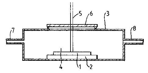
Figure 1 shows a cross-section of part of an
arrangement for etching the substrate; and
Figure 2 shows a cross-section of a groove produced in
the substrate by etching according to the method.
The figures are schematic only and are not drawn to
scale.
Referring to figure 1, in order to etch the substrate
l it is mounted on a support 2 in a cell 3. The cell 3 is
provided with a u-v transparent window 6 and a laser (not
shown) ic mounted so that its beam 5 passes through the
window 6 and impinges on the substrate 1. A gas mixture 4
flows through the cell 3, via an inlet 7 and an outlet 8,
over the substrate 1.
The laser is an excimer laser operating on Krf at
248nm. It is suitable for pulsed operation at a rate of
100 pulses/sec each 10~ secs long. The radiation has an
~,. ;
~.Z~56~3
-- 6 --
energy of 2.5 x 10 ~ Joules per pulse. The beam 5,
wh~ch is partlally focussed, irradiates an area of the
substrate of 5 x 10 8cm2, the power delivery being
50 watts/cm .
' 5 The material of the substrate 1 is undoped InP
oriented in a (100) plane and the substrate 1 is in the
form of a wafer of material 200 to 300~m deep.
In carrying out the method of the invention, a mixture
of methyl iodide and hydrogen is supplied to the cell 3
o such that it flows over the substrate 1 at a rate ly~ng in
the range from 10 to 100cm3/min, inclusive. The partial
pressure of methyl iodide in the mixture lies ~n the range
from 1 to 100 Torr incluslYe and the partial pressure of
hydrogen in the mixture makes up the difference between
that and atmospheric pressure, 760 Torr.
The spot of the laser beam 5 is scanned over the
substrate 1 at a rate of O.Z~m/sec in the presence of the
gas mixture.
As a result of the above scanning, it has been
observed that an etched groove 9 is generated in the
substrate 1, having a depth of about 1~ and a width of
2~m. The bulk rate of removal of the substrate material
is therefore 0.4~m3/sec and the etch rate in terms of
maximum groove depth is about 85nm/sec. This compares
well with that quoted by Ehrlich et al.
Referr~ng to figure 2, the cross-section of the groove
9 produced has been found to be approximately Gaussian.
This appears to reflect the intensity profile of the
partially focussed laser beam. Varying the lntensity
profile of the beam would then vary the cross-sect~on of
the groove 9 produced.
The reactions which cause the etching to occur under
.
~.~i756~3
the condltions described above are considered to be as
~ollows:
(i) CH3I CH3
(li) InP ~ nl = InIn + P
That is, the methyl iodide dissociates under the
action of the laser beam to generate iod~ne free
radicals. The iodine free radicals in turn displace the
phosphide ions from the substrate, the resulting ~ndium
iodide and the phosphorous species evaporating from the
o substrate surface.
The phosphorous species is shown as P, but it is
probably present as P2 or P4. However, at the
temperatures generated by the laser beam, P4 is thought
to be unlikely.
1S It is suggested, without in any way intending to limit
the scope of the present invention, that the use of an
oxygen-free reducing environment during the etching
process prevents the generation of an involatile oxide
fil~ on the substrate caused by traces of 2 The
eff~ciency of the etch~ng would then be ~ncreased by
preserving the volat~llty of the react~on products.
It has been proposed to etch us~ng an abmosphere of
helium and halide gas. However, even a small amount of
oxidising agent can exert an adverse e~fect and it is
extremely d~fficult in practice to avoid ingress of
oxidising agents, particularly oxygen. The presence of a
reduc~ng agent, eg hydrogen, controls the effect of such
impurities.
The concentration of hydrogen ~n the gas mixture of
the embodiment described above was selected to be
sufficlently hlgh to suppress the effect of any 0~
leaking into the system. Since the react~on of the H2
W~t1l the 2~ whlch does not normally occur to any
6~
significant degree at room temperature, is promoted by the
light source, the minimum concentration of hydrogen used
should only need to be twice the equilibrium concentration
of oxygen present during etching. With existing
technology for making the system leakproof, the minimum
pressure of` hydrogen which should be used is then 10
Torr.
Although the use of a pulsed laser beam is described
above, significantly improved etch rates may be
achieved by the use of a continuous wave operaticn laser.
For instance a frequency doubled Ar ion laser operating
continuously at ~57nm could be used.
There are alternative ways in which to produce a
reducing environment. For instance the hydrogen might be
: 15 replaced by carbon monoxide.
Methyl iodide is not the only gas with which etching
can be carried out, other gaseous halides also being
effective. For instance methyl bromide or ethylene
dibromide could replace the methyl iodide in the method.
Howeverg methyl iodide is relatively convenient to use,
being slightly less volatile than at least methyl bromide
and therefore being less likely to have a toxic effect.
; Further, methyl iodide shows stronger u-v absorption than
methyl bromide and therefore has a more efficient
interaction with the light. (The etch rate quoted above
may of course be altered by replacing methyl iodide with
another gas).
Other III - V materials may be etched as well as
indium phosphide. For instance, GaAs, GanlAs, or the
quaternary materials in InxGaO xAsyPO y might be
etched by the method described.
Although the preferred method relies on the use of a
laser, the light may be provided by a different source
1.2~751Ei~3
such as by a u-v lamp. Where thls is the case, the
concentrat~on of hydrogen, or other component used to
create a reducing environment, may have to be lncreased ~n
order to be effective ln suppressing the formation of
ox~de films. This ls llkely to be the case if the
temperature produced during the process at the substrate
surface ls relatively low: an excess of hydrogen w~ll be
required ln order to drlYe forwards the H2/02 reaction.
Methods of etchlng ascording to embodiments of the
o present invention may be used in the production of a wide
variety of opto-electronic devices including waveguide
devices, detectors and lasers.